Optical simulation design of surface mounted device beads for wide beam and high uniformity display
2024-02-05WEIWeiCHENZhizhongGUOHaozhongJIAChuanyuFANGFangZOUJunFANGQianWUYouSUNMinghaoLIQianKUANGYuhanYINQikaiZHANGGuoyi
WEI Wei ,CHEN Zhi-zhong,GUO Hao-zhong,JIA Chuan-yu,FANG Fang,ZOU Jun,FANG Qian,WU You,SUN Ming-hao,LI Qian,KUANG Yu-han,YIN Qi-kai,ZHANG Guo-yi
(1.Yancheng Teachers University, Jiangsu Intelligent Optoelectronic Device and Measurement and Control Engineering Research Center, Yancheng 224007, China;2.School of International Academy of Microelectronics, Dongguan University of Technology, Dongguan 523000, China;3.Gold Medal Analysis, Guangzhou 511338, China;4.College of Physics, Peking University, Beijing 100871, China;5.Department, Dongguan Institute of Opto-electronics, Peking University, Dongguan 523808, China;6.Semiconductor Research Center, Hon Hai Research Institute, New Taipei city 236, China;7.Shanghai Institute of Technology, Shanghai 201418, China)
Abstract: Through analysing the optical requirements of wide beam and high uniformity light beads,which are currently used in displays,and packaging micro Light-Emitting Diode (LED) chips with a novel non-Lambertian distribution,we realized the production of wide beam and high uniformity micro-LED chip light beads.The light output efficiency and beam angle of fixed beads were simulated using brackets made of copper,titanium,aluminium and silver,as well as materials that were completely reflecting and absorbing.The simulations were conducted at various fixture angles,packaging heights,packaging materials,sapphire thicknesses,and patterned sapphire substrate sizes.By adjusting the chip and packaging parameters,we can obtain one,two,or three light beams with Surface Mounted Device (SMD) lamp beads characteristics that provide wide angles,high uniformity,and far-field light distribution.These characteristics can meet the current display requirements for LED and LCD.
Key words: non-lambertian distribution;lambertian distribution;displays;SMD lamp beads
1 Introduction
Backlight displays that use Light-Emitting Diode (LED) and Liquid-Crystal Display (LCD) technologies have several advantages such as high energy efficiency and improved contrast,low cost,and a better spliceability[1-7].Consequently,these displays have entered a stage of rapid development.However,backlight displays using LED and LCD technologies have certain drawbacks,including the inability to be fabricated in ultra-thin formats[8-10].This impedes the utilization of various backlight displays,such as laptops and mobile phones,in ultrathin display technology.
The term “micro-LEDs” refers to LEDs that have chip sizes smaller than 100 μm×100 μm[11].Research has shown that micro-LED chips exhibit high uniformity and wide beam angles,thereby enabling their deployment in ultrathin displays.However,certain difficulties hinder the direct installation of micro-LED chips on display screens.Typical solution is to install a micro-LED chip directly on a Chip-On-Board (COB),and then create a display by splicing the COB or SMD LED+LCD.However,COB technology has seveval disadvantages,including difficulties in achieving its primary optical design.Many COB-based devices use secondary optical designs and lenses to adjust the mixing distance,which makes it difficult to achieve ultrathin mixing distances[12-14].The integration of micro-LED chips into COBs through display technology remains under research and has not yet been widely adopted.After reviewing pre-existing technical methods,we propose a technological path that combines micro-LED chips with Surface-Mount Technology (SMT) packaging to fulfil the current demand for ultrathin displays and mounted devices.As typical LEDs follow the Lambert distribution[15-20],the illumination is stronger at mid-angles but weaker on both sides.The optical design of supplementary lighting requires consideration of modifications to light direction and redistribution of intensity,in conjunction with using precision optical lenses which poses significant challenges to image processing.Numerous studies reveal that under certain conditions[21-23],micro-LEDs conform to a non-Lambert distribution and have uniform light distributions[24-25].It would be advantageous to develop lowcost,standard SMD beads that generate wide-beam and large-angle light output.Using these beads in displays reduces the reliance on lenses and mixing distances,thus providing a better display experience.The objective of this study is to determine an appropriate parameters that satisfies the optical requirements of displays that utilize large-angle,highuniformity SMT beads with micro-LED cells to minimize cell sizes and costs.In addition,micro-LEDs minimize the mixing distance and produce ultrathin displays.
To perform optical simulations,we implemented the Monte Carlo approach in conjunction with the ray-tracing method using TracePro software.Figure 1 presents a detailed illustration of the specific model,and a schematic of the structure of the SMD lamp bead is shown in Figure 2.For the purpose of this study,we set 0° as the direction perpendicular to the light-emitting plane in front of the chip and downward.This study suggests that an optical design for LED+lenses can be achieved through simulation calculations using a new patch LED.The optical design technology of the novel patch LED can meet display requirements by reducing material costs,light loss,weight,and shortening the mixing distance.
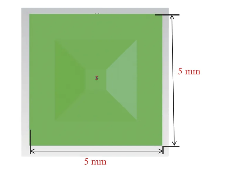
Fig.1 Top view of the LED device structure rendered using TracePro software
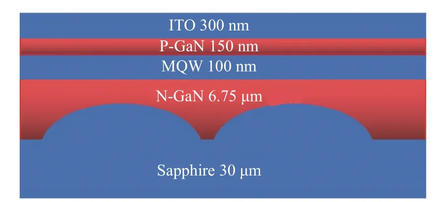
Fig.2 Sectional view of the unpacked micro-LED device structure
Table 1-3 present the model parameters.The refractive indices of sapphire,N-type GaN,MQW,P-type GaN,and ITO were 1.7,2.45,2.54,2.45,and 1.5,respectively.The absorption coefficients of sapphire,N-type GaN,MQW,P-type GaN,and ITO were 0.004,2.3,25,2.3,and 0 mm-1,respectively.The thicknesses of the sapphire,N-type GaN,MQW,P-type GaN,and ITO layers were 30,6.75,0.1,0.15,and 0.3 µm,respectively[23,26-29].Micro-LED chips with diameters of 10,20,30,40,and 50µm were fabricated,while sapphire beads with diameters of 2,3,and 4 µm were constructed as hemispherical microstructures.SMD lamp-bead holders of 5 mm× 5 mm were designed interiors featuring a four-sided conical platform inclined at angles of 5°,15°,25°,35°,45°,55°,65°,75°,and 85°.The chip size was 30 µm,with packaging heights of 10,20,40,60,and 80 µm.Brackets were fabricated using various materials including copper,aluminium,silver,and titanium,along with fully absorbing and fully reflective materials.The refractive and absorption indices of each material are listed in Table 1.For packaging,epoxy,PMMA,and silica were used with their respective refractive and absorption indices listed in Table 2[30]for a 30 µm chip.All chips used were micro-LED chips with suitable packaging sizes in accordance with the 5 050 chip packaging requirements.The structure of the LED device is depicted in Figs.1-3.The wave-length of SMD LED is 450 nm,and the distance between the sample and the detector is about 1 000 mm.To calculate light extraction efficiency,we divide the number of photons emitted to the outside of the SMD per unit time by the number of photons emitted by the active region per unit time.
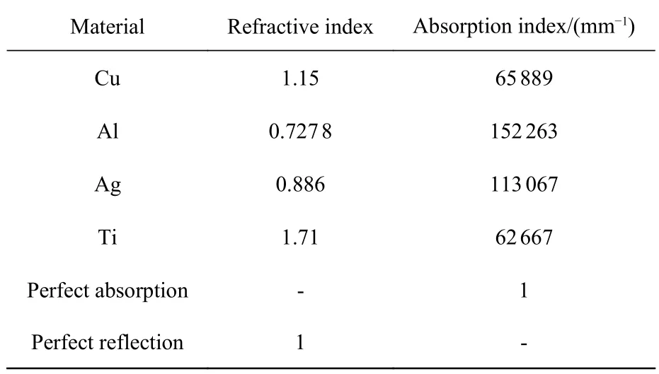
Tab.1 Simulated optical parameters of different bracket materials
Tab.2 Simulated optical parameters of different packaging materials

Tab.3 Simulated optical parameters of light-emitting diodes with different sizes
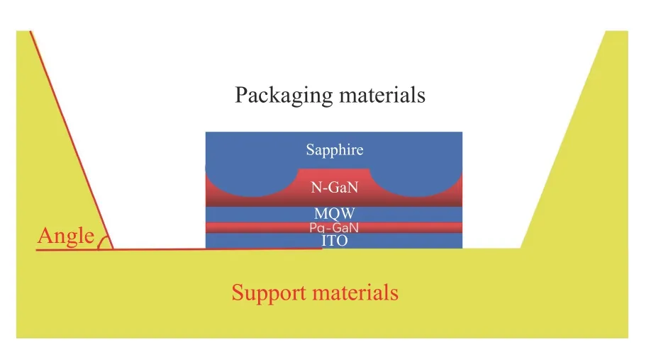
Fig.3 Sectional view of the packaged 5050 SMD beads.
Figs 1 to 3 show images of the unmodified chip’s original structure used in this study.Figure 1 depicts a top view of the packaged 5 050 chip rendered in TracePro software.Figure 2 shows a cross-sectional view of the structure of the unpackaged chip,and Figure 3 offers a cross-sectional view of the packaged 5 050 chip.The size of the chip was set to 10 µm.The inclination angle of the internal packaging was altered across a range of 5°-85°.The beam angles and output efficiencies of the SMD LEDs were simulated and calculated for inclination angles of 5°,15°,25°,35°,45°,55°,65°,75°,and 85°.An assembly comprising Al support material,PMMA packaging material and a chip size of 10 µm was simulated with a fixed inclination angle of 85°.The resulting calculations included the beam angles and output efficiencies of SMT LEDs of 10,20,40,60,and 80 µm,with different packaging heights.The SMD with a packaging height of 0.05 mm was analyzed by fixing the inclination angle at 85° and utilizing Al as the support material and PMMA,epoxy,and silicone as the packaging materials.This analysis resulted in the calculation of the beam angle and output efficiency.The chip size was set to 30 µm with a fixed inclination angle of 85°.The support material was changed from Cu to Al,Ag,and Ti.The inner cone of the packaging was set to full absorption and reflection while utilizing silicone as a packaging material.Therefore,the beam angle and output efficiency of a 0.08 mm high packaged SMD were calculated.At an 85° fixed inclination angle,the bracket was made of Al and PMMA was used as the packaging material.We calculated the beam angle and output efficiency of a 0.1 mm high SMD package at chip sizes of 0.01,0.03,0.05,and 0.1 mm.It is noteworthy that the size of the transformed chip is relatively large when the angle is 85°,which allows for the largest possible placement area in the middle position of the chip.In the following simulation,we set the fixed inclination angle to 85°,the bracket material to Al,the packaging material to PMMA,and the thickness of the sapphire substrate to 0.03 mm.We changed the microstructure dimensions on the sapphire substrate to 0.002,0.003,and 0.004 mm and then calculated the beam angle and output efficiency of a 0.1 mm high packaged SMD for packaging.Finally,a simulation was conducted with an inclination angle fixed at 85°for the aluminium bracket material,and PMMA was used as the packaging material.The beam angle and output efficiency of an SMT LED with a packaging height of 0.08 µm were calculated for sapphire thicknesses at 0.01,0.03,and 0.05 mm.
2 Optical simulation results and analysis
Table 4 shows the results for the 5 050 SMT beads with Al bracket and PMMA packaging materials at different angles.It is evident that at the inclination angles of 45°,55°,and 65°,the chip size measured 10 µm,and the far-field light distribution of the SMD LED emitted a single beam.These outcomes were confirmed at beam angles of 160°,140°,and 120°.The far-field light distribution of the SMD LED emitted a dual beam at the angles of 5,15,25,35,75,and 85°,as depicted in Figure 4.The corresponding beam angles were 70° × 2,50° × 2,70° × 2,70° × 2,50° × 2,and 30° × 2,respectively.Fig.4 shows how the light extraction efficiency first increased and then decreased as the inclination angle increased.The highest light extraction efficiency,at 0.654,was achieved when the inclination angle was 65°.
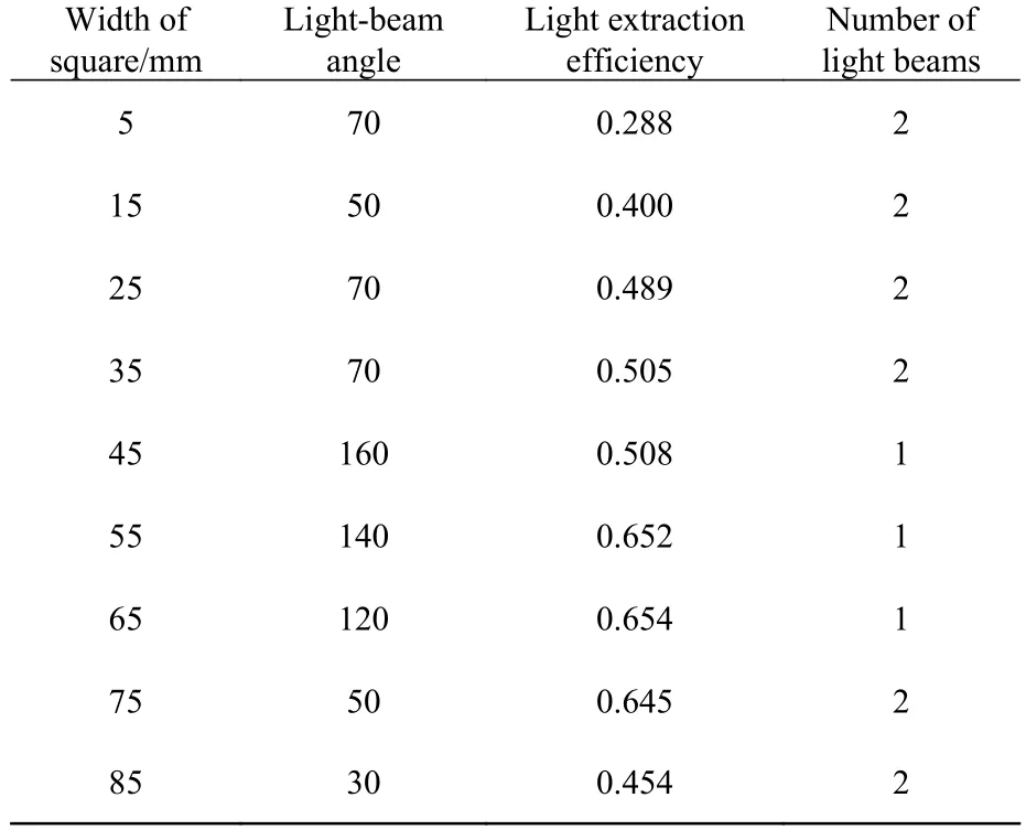
Tab.4 Far-field beam angle and output efficiency of 5050 SMT beads with Al bracket and PMMA packaging materials at different angles

Fig.4 Schematic diagram of far-field light distributions of 5050 surface-mount technology (SMT) beads with Al brackets and PMMA packaging material at different inclination angles
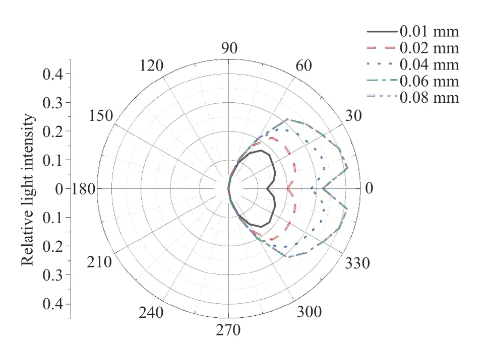
Fig.5 Far-field light distributions of 5050 SMT beads with different packaging heights,Al brackets,and PMMA packaging materials at an inclination of 85°.
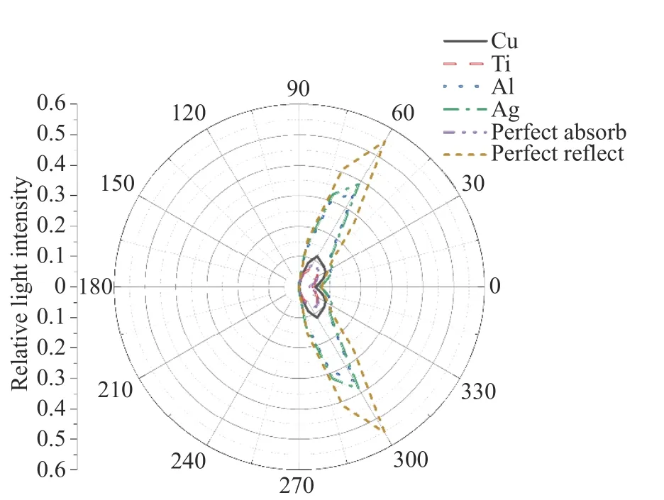
Fig.6 Far-field light distributions of 5050 SMT beads with different support materials,a packaging height of 0.08 mm,and Al support at an inclination of 85°

Fig.7 Far-field light distributions of 5050 SMT beads with different material supports and silicone,a packaging height of 0.08 mm,and a sapphire thickness of 0.05 mm at an inclination angle of 85°

Fig.8 Far-field light distributions of 5050 SMT beads with different chip sizes and Al brackets,and PMMA packaging materials at an inclination angle of 85°
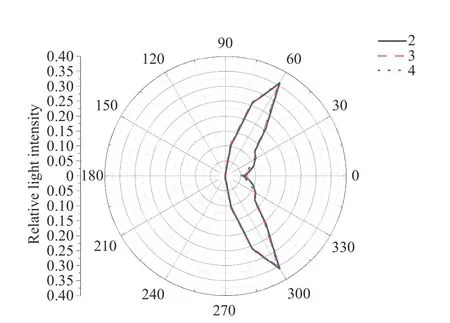
Fig.9 Far-field light distributions of 5050 SMT beads with a sapphire thickness of 30 μm Al brackets,and PMMA packaging materials at an inclination angle of 85°.
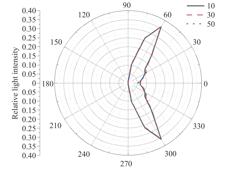
Fig.10 Far-field light distributions of 5050 SMT beads with different sapphire thicknesses,Al brackets and PMMA packaging materials at an inclination of 85°
Table 5 lists the results for 10 µm chips with different packaging heights.The far-field light distribution of the SMD LED is a single beam at packaging heights of 0.01,0.02,0.04,0.06,and 0.08 mm.Figure 5 verifies this for beam angles of 160°,140°,140°,and 120°.When the packaging height decreased,the beam angle of the packaged chip LED increased from 120° to 160°,however,the light output efficiency decreased from 0.638 to 0.369.

Tab.5 Far-field beam angles and output efficiencies of 5050 SMT beads with different packaging heights and Al brackets and PMMA packaging material at an inclination of 85°
Table 6 presents the outcomes for 30 µm chips packaged with different materials.A dual beam was observed in the far-field light distribution of the SMT LED when the packaging material or the inner surface of the package was made of aluminium,silver,or completely reflective materials.This is confirmed in Figure 5,and the corresponding beam angles were 20° × 2,20° × 2,and 30° × 2,respectively.When the packaging material or inner surface of the package consisted of copper,titanium,or fully absorptive materials,the far-field light distribution of the SMD LED produced a single beam,as displayed in Figure 6.The corresponding beam angles measured 140°,160°,and 120°,respectively.According to Table 6,the maximum light output efficiency was 0.813 when the inner surface of the package was fully reflective,and 0.175 when it was fully absorptive.
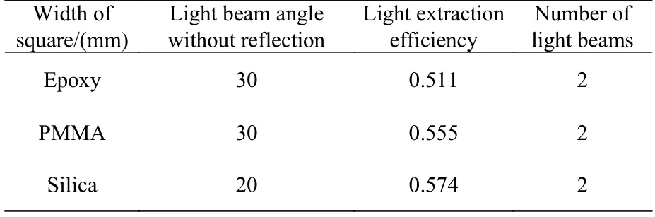
Table 7 presents the outcomes for silicone-supported beads with varying packaging materials.The far-field light distribution of the SMD LED was observed to be a dual beam when the packaging material or inner surface was made of epoxy,PMMA,or silica.Figure 7 confirms this for the beam angles of 30° × 2,20° × 2,and 30° × 2,respectively.When silicone was used as the packaging material,the light extraction efficiency reached a maximum of 0.874,and when epoxy was used as the packaging material,the light extraction efficiency reached a minimum of 0.511.

Tab.6 Far-field beam angles and output efficiencies of 5050 SMT beads with different packaging materials,and a packaging height of 0.08 mm,Al brackets at an inclination of 85°
Tab.7 Far-field beam angles and output efficiencies of 5050 SMT beads with different materials,a packaging height of 0.08 mm,and a sapphire thickness of 0.05 mm packaged with silicone supports at an inclination of 85°
Table 8 presents the results obtained for chips with a sapphire thickness of 10 μm,Al brackets,and PMMA packaging material at an inclination angle of 85°.The far-field light distribution of the SMD LED was a dual beam when the chip dimensions were 0.03,0.04,0.05,or 0.1 mm.Figure 8 confirms this,with the corresponding beam angles being 30° × 2.Furthermore,as the chip size decreased,the light output efficiency increased from 0.456 to 0.521.

Tab.8 Beam angles and output efficiencies of 5050 SMT beads with different chip sizes and Al brackets and PMMA packaging materials at an inclination of 85°
Table 9 shows the findings obtained from using Al brackets to fix 30 μm sapphire-thick beads with PMMA packaging material at an inclination angle of 85°.The sapphire substrate has hemispherical microstructures with diameters of 0.002,0.003,and 0.004 mm.Each case led to the acquisition of dual-beam far-field SMT LED light distributions,as shown in Figure 9.This is confirmed in Figure 9 with corresponding beam angles of 30° × 2.As the chip size decreased,the efficiency of light output increased from 0.553 to 0.555.

Tab.9 Beam angles and output efficiencies of 5050 SMT beads with a sapphire thickness of 30 μm,Al brackets,and PMMA packaging materials at an inclination angle of 85°
Table 10 presents the outcomes obtained while using beads with Al brackets and PMMA packaging material at an inclination of 85° with the sapphire thicknesses varying from 0.01,0.03,and 0.05 mm.In all instances,there were SMT LED,dual-beam,and far-field light distributions,as confirmed by Figure 10,showing corresponding beam angles of 30° × 2.As the chip size decreased,the light output efficiency increased from 0.553 to 0.547.
The simulation results indicate that variations in reflection angles and materials impact the number of light beams.

Tab.10 Beam angles and output efficiencies of 5050 SMT beads with different sapphire thicknesses and Al brackets and PMMA packaging materials at an inclination angle of 85°
3 Conclusion of optical simulation
The simulations conducted in this study revealed that using silicone packaging material resulted in the highest light output efficiency.Moreover,employing completely absorptive packaging materials on the inner cone improved output efficiency,while using wholly reflective surface materials decreased it.As the angle of the cone within the package increased,the output changed from dual-beam to single beam and then back to the dual-beam.Also,when the angle of the inner cone of the package increased,the light output efficiency first increased,peaked at 65°,and then fell.Although reduction in chip size led to increased light output efficiency,the light extraction efficiency witnessed a riseand then plateaued as the sapphire thickness increased.Finally,as the diameter of the microstructure in the rear hemisphere of the sapphire substrate increased,there was a slight reduction in the efficiency of light output.