W-doped In2O3 nanofiber optoelectronic neuromorphic transistors with synergistic synaptic plasticity
2023-12-02YangYang杨洋ChuanyuFu傅传玉ShuoKe柯硕HangyuanCui崔航源XiaoFang方晓ChangjinWan万昌锦andQingWan万青
Yang Yang(杨洋), Chuanyu Fu(傅传玉), Shuo Ke(柯硕), Hangyuan Cui(崔航源),Xiao Fang(方晓), Changjin Wan(万昌锦),‡, and Qing Wan(万青),2,§
1School of Electronic Science&Engineering,and Collaborative Innovation Center of Advanced Microstructures,Nanjing University,Nanjing 210023,China
2School of Micro-Nano Electronics,Hangzhou Global Scientific and Technological Innovation Center,Zhejiang University,Hangzhou 310027,China
Keywords: W-doped In2O3 nanofibers,neuromorphic transistors,optoelectronic synaptic plasticity
1.Introduction
In the current post-Moore era, the simulation of the perception and computing functions of synapses and neurons by artificial neuromorphic devices has attracted increasing attention.[1]Over the past few decades, many types of neuromorphic devices have been proposed to emulate synapses/neurons.[2,3]Among them, nanofiber optoelectronic synapse transistors are novel electronic devices that combines the benefits of optics,electricity,and nanotechnology.[4,5]Optical signal has significant advantages in high-speed transmission,high stability and efficient connection of separated modules.Therefore, nanofiber optoelectronic synapse transistors have higher switching speed, smaller size, lower power consumption,and greater reliability comparing with other synaptic devices.[6–8]In the meantime, multi-functional synaptic plasticity can be achieved in a single synaptic device through photoelectric synergy, greatly simplifying the artificial neural network (ANN) with improved the robustness and scalability.[7]What is more, a stronger light-guiding effect may be exhibited by nanofibers with higher surface area,which can be beneficial for simulating synaptic plasticity and can enrich the diversity of neural network designs.[9]Therefore,the nanofiber optoelectronic synapse transistors with synergistic synaptic plasticity may have promising applications in ANN for neuromorphic computing.[10–13]
Indium oxide (In2O3) is a wide bandgap (3.75 eV)semiconductor material with high electron mobility (theoretical value∼270 cm2·V-1·s-1) and high transparency,and it has been widely used in semiconductor optoelectronic devices.[14–16]Recently,efforts have been made to improve its properties by doping elements such as Sn,[17]Mo,[18]Ga,[19]Zn,[20]and so on.Among them,W-doped In2O3(IWO)have recently gained interest following the experimental demonstration of IWO field effect transistors with ultra-high on/off current ratio.[21–25]The high valence difference between W6+and In3+may be particularly advantageous for facilitating the transfer of electrons.[26]Moreover, W has high oxygen bond dissociation energy, even low doping concentration of W can inhibit the excess oxygen vacancy, thus improving the electrical performance of the device.[27]Therefore,IWO can be a promising candidate for future channel material of transistors.
Here, we employed the highly efficient and controllable electrospinning method to prepare IWO nanofibers, and its simple schematic illustrated in Fig.1(a).Under a high-voltage electric field, polymer solution is sprayed through a nozzle,forming fiber-shaped droplets or streamlines in the air, and ultimately resulting in nanofiber formation on the electrode.Subsequently, by combining with the fabrication process of synaptic transistors,IWO nanofibers synaptic transistors were successfully constructed.The long-term plasticity of the transistor was successfully demonstrated using light pulses as input signals.Furthermore,the synaptic weight can be precisely regulated by the light and electrical signals.Our results are very interesting for the development of nanofiber neuromorphic systems.
2.Experimental details
A solution was prepared by dissolving 0.3 g of indium nitrate (In(NO3)3·xH2O, Aladdin) in 10 ml of N, Ndimethylformamide(DMF,Aladdin),which was then stirred at 50◦C for 1 h.A specific amount of tungsten chloride(WCl6,Meryer)was added to the solution,with a molar ratio of W:In set to 5 mol%.After stirring for 1 h,2.0 g of polyvinylpyrrolidone (PVP, Aladdin, Mw=1.3×10⁶) was added to the solution and stirred overnight to form a clear and uniform solution.Electrospinning was employed to fabricate homogeneous nanofiber films on an(aluminum oxide)Al2O3/Si substrate.To ensure good contact between the nanofiber film and the Al2O3/Si substrate, the sample was baked at 150◦C for 15 min and then treated under an ultraviolet lamp for 45 min.The PVP polymer was removed from the nanofibers by annealing at 500◦C for 2 h,resulting in crystalline IWO nanofibers.Finally,the Al films with thickness of 100 nm were deposited by thermal evaporation for severing as source–drain electrodes using a shadow mask.The channel length and width of the IWO nanofiber optoelectronic synapse transistors are 80 µm and 1000 µm respectively.The size of the source/drain electrodes are all 150µm×1000µm.The morphology and composition of IWO nanofibers were analyzed respectively using a scanning electron microscope (SEM, JEOL, JSM-7000F)and x-ray photoelectron spectroscopy (XPS, ThermoFisher 250Xi).We used a semiconductor parameter analyzer(Keithley 2636B)and a fiber-coupled laser module(Changchun New Industry(CNI)Laser PGL-FC-360 nm)to investigate the electrical characteristics and neural morphology functions of photoelectric synaptic transistors based on IWO nanofibers.
3.Results and discussion
The morphology of IWO nanofibers after hightemperature annealing was analyzed using scanning electron microscopy (SEM), as illustrated in Fig.1(b).And the magnified view inset reveals IWO nanofibers diameter of approximately 80 nm.Next, the chemical states of In and W atoms in the IWO nanofibers were detected using XPS,as shown in Figs.1(c) and 1(d), respectively.The binding energies of In 3d3/2and In 3d5/2were 452.3 eV and 444.7 eV,respectively,which match well with In3+ions in In2O3.[28]The W 4f5/2and W 4f7/2peaks at 38.1 eV and 35.8 eV, respectively, can be attributed to the existence of W6+in the IWO nanofibers(Fig.1(d)).The W 4f5/2and W 4f7/2peaks both appeared as doublets, possibly due to the presence of other valence states of W,as described in other literature.[29]

The schematic diagram of biological neurons and synapse is illustrated in Fig.2(a).Biological synapses are mainly composed of presynaptic membrane, synaptic cleft, and postsynaptic membrane.[30]The synaptic cleft contains a substantial amount of neurotransmitters.Upon stimulation of the presynaptic membrane, the neurotransmitter in the synaptic cleft is released and diffuses to the postsynaptic membrane, completing the information transmission.[31]The IWO nanofibers transistor can simulate the biological synapses, and its structure diagram is shown in Fig.2(b).The bottom gate(silicon)and the light source(360 nm)are utilized to simulate the presynaptic input,while the source/drain electrodes function as the postsynaptic output.The transfer characteristic curve of the transistor is shown in Fig.2(c),with the gate voltage scanned from-2 V to 3 V, whileVDSis fixed at 2 V.An anticlockwise hysteresis is evident, and theION/IOFFratio is around 2.2×10⁵.
A typical light induced excitatory postsynaptic current(EPSC) is stimulated by applying an optical pulse (25 ms,0.04 nW/µm2),as shown in Fig.3(a).EPSC increased rapidly to 10.27 nA under the light pulse, and then exhibited a slow decay.Because electrons could be generated in the channel when the IWO nanofiber channel is stimulated by the light pulse, and eventually the channel conductance will be increased.When the light pulse is finished, the conductance of the IWO nanofiber channel will not be reduced to the initial value.This phenomenon is commonly referred to as the persistent photoconduction effect.This the intrinsic mechanism of long-term synaptic plasticity in our device.Subsequently,the influences of light intensity and pulse width on the EPSC were investigated, as shown in Fig.3(b).Eight light pulses with different widths and three power densities of 0.04 nW/µm2,0.34 nW/µm2,and 0.66 nW/µm2were measured.When light power density is 0.04 nW/µm2, the EPSC value is very low due to the very small photoconduction effect.The maximum EPSC can reach 144.19 nA and 342.62 nA when the light power densities are 0.34 nW/µm2and 0.66 nW/µm2, respectively.In addition,when the pulse width is the same,the EPSC increases with the increase of light power density.Similarly,at the same light power density,EPSC increases linearly with increasing pulse widths(Fig.3(c)).In general, the long-term potentiation(LTP)can be achieved through repeated training.The increase of pulse numbers could lead to the enhancement of synaptic weight.Three sets of light pulses(0.34 nW/µm2,25 ms, andVDS=0.1 V) with different numbers (300, 600,and 1000) were designed to emulate this process (Fig.3(d)).When the light pulse numbers are 300,600,and 1000,the EPSCs increase to 63.58 nA,129.11 nA,and 243.70 nA,respectively.Moreover, when light pulse is finished, the retention rates after 10 seconds are 69.99%, 84.07%, and 90.86% for light pulse numbers of 300,600,and 1000.Assuming that the decay time of EPSC corresponds to the time course of forgetting after learning, the retention rate of the learning outcome will increase with the increase of learning number.
To investigate the synergistic synaptic plasticity of IWO nanofiber optoelectronic synapse transistor, electrical signals were applied to the bottom gate (silicon) while optical signals were applied to the IWO nanofibers channel to trigger the EPSCs.The EPSCs of the transistor were measured under the same light intensity (0.34 nW/µm2) and at differentVGSof-0.2 V,-0.1 V, 0 V, and 0.1 V for 7 s.The light pulse width was fixed at 300 ms.Figure 4(a)shows the normalized conductance decay behaviors of the IWO nanofibers channel under differentVGS.The application of a positiveVGSleads to an increase in the electron density in the IWO nanofiber channel layer, consequently causing a rise in EPSC.The electron density in the IWO nanofibers channel layer decreases when a negativeVGSis applied, resulting in a decrease in EPSC.Figure 4(b) shows the synaptic weight variation curve of the device after applying differentVGSfor 7 s.AsVGSincreases from-0.2 V to 0.1 V,the synapse weight increases from 4.7%to 96.2%.According to the accumulation and consumption of electrons at the IWO/Al2O3interface, the band bending diagram is shown in Fig.4(c).Under light illumination, the ionization of oxygen vacancies induces an excess of electrons(VO→V+O+ e-and VO→V2+O+2e-), thereby increasing the IWO conductivity.When the light is finished, whenVGS>0,it provides additional electrons that reduce the recombination rate of photogenerated electrons(V2+O+2e-→VO),and a relatively higher normalized conductance value can be observed.[32,33]Conversely (VGS< 0), the recombination of photo-induced electrons is accelerated, and a relatively low normalized conductance is maintained.Therefore,the synaptic plasticity of the IWO nanofiber optoelectronic synapse transistors can be synergistic modulation by optical and electrical signals.

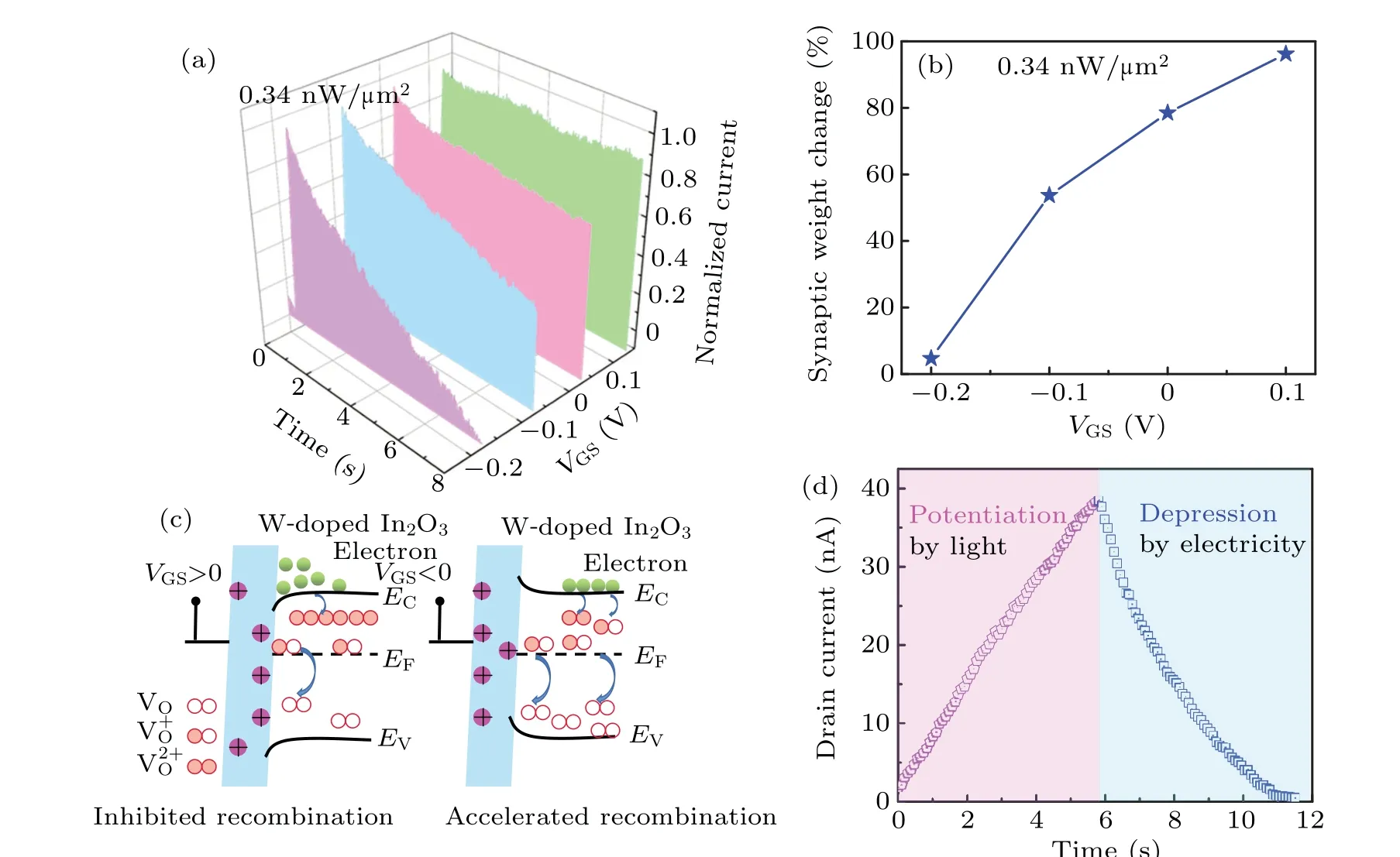
The long-term potentiation (LTP) and long-term depression(LTD)are also important parameters of synaptic plasticity.Combining the results of light-induced potentiation and voltage-induced depression,the transition from LTP to LTD in biological synapses was emulated,as shown in Fig.4(d).The EPSC increased to 38.23 nA by continuously applying 64 light pulses (∆t=90 ms, 0.34 nW/µm2), emulating LTP behavior in the biological synapse behavior.Then,the light source was turned off and 64 electrical pulses(∆t=90 ms,VGS=-0.3 V)were applied to the device,reducing the EPSC to 0.53 nA.The transformation process of the synaptic weight updating,which is significant for the construction of artificial neural networks.
To better visualize the synaptic plasticity of photoelectric synergistic modulation, a 5×5 device array was simulated,and the results are shown in Fig.5.From Fig.5(b), “N” is clearly written into the array, when the light signal is applied to the device.After a period of time,the“N”symbol can still be maintained in the array (Fig.5(c)), corresponding to the long-term memory of the system.Then, the image memory in the system was erased using an electrical signal(Fig.5(d)).After the erasure operation, the system returned to its initial state.Since the system can exhibit “write–erase” processes according to different sequence pulse stimulations,the system has a certain degree of robustness.

4.Conclusion and perspectives
In summary, we successfully prepared IWO nanofibers using electrospinning method and fabricated optoelectronic neuromorphic transistors with synergistic synaptic plasticity.Some important synaptic functions such as EPSC, long-term plasticity, and multipulse facilitation, have been studied in IWO nanofiber optoelectronic synapse transistors.Moreover,the long-term retention in the characterization of electrical parameters of electronic synaptic devices can be emulated by repeated pulsed stimuli.Importantly,a reliable conversion from light-induced LTP to electrically induced LTD can emulate the learning and forgetting processes in the human brain.Our results indicated that nanofiber optoelectronic synapse transistor is promising for artificial neural network construction.
Acknowledgements
Project supported by the National Key Research and Development Program of China (Grant Nos.2021YFA1200051 and 2019YFB2205400) and the National Natural Science Foundation of China(Grant Nos.62174082 and 62074075).
猜你喜欢
杂志排行

Chinese Physics B的其它文章
- Optimal zero-crossing group selection method of the absolute gravimeter based on improved auto-regressive moving average model
- Deterministic remote preparation of multi-qubit equatorial states through dissipative channels
- Direct measurement of nonlocal quantum states without approximation
- Fast and perfect state transfer in superconducting circuit with tunable coupler
- A discrete Boltzmann model with symmetric velocity discretization for compressible flow
- Dynamic modelling and chaos control for a thin plate oscillator using Bubnov–Galerkin integral method