Double-slot ultra-compact polarization beam splitter based on asymmetric hybrid plasmonic structure
2023-10-07WANGFangLIUHuaMATaoMAShoudaoLIUYufang
WANG Fang,LIU Hua,MA Tao,MA Shou-dao,LIU Yu-fang
(1.College of Electronic and Electrical Engineering, Henan Normal University, Xinxiang 453007, China;2.Henan Key Laboratory of Optoelectronic Sensing Integrated Application, Xinxiang 453007, China;3.Academician Workstation of Electromagnetic Wave Engineering of Henan Province,Xinxiang 453007, China;4.Henan Engineering Laboratory of Additive Intelligent Manufacturing, Xinxiang 453007, China)
* Corresponding author,E-mail: lh18237269109@163.com
Abstract: To improve the extinction ratio of a polarization beam splitter, we propose a dual-slot ultra-compact polarization splitter (PBS) consisting of a hybrid plasma Horizontal Slot Waveguide (HSW) and a silicon nitride hybrid Vertical Slot Waveguide (VSW).The coating material is silicon dioxide, which can prevent the oxidation of the mixed plasma and also facilitate integration with other devices.The mode characteristics of the HSW and VSW are simulated by using the Finite Element Method (FEM).At suitable HSW and VSW widths, the TE polarization modes in HSW and VSW are phase-matched, while the TM polarization modes are phase mismatched.Therefore, the TE mode in an HSW waveguide is strongly coupled with a VSW waveguide by adopting a dual-slot, while the TM mode directly passes through the HSW waveguide.The results show that PBS achieves an Extinction Ratio (ER) of 35.1 dB and an Insertion Loss (IL) of 0.34 dB for the TE mode at 1.55 μm.For the TM mode, PBS reached 40.9 dB for ER and 2.65 dB for IL.The proposed PBS is designed with 100 nm bandwidth, high ER, and low IL, which can be suitable for photonic integrated circuits (PICs).
Key words: photonic integrated circuits; polarization beam splitter; slot waveguides.
1 Introduction
In recent years, sub-micron waveguide devices have been realized using the large difference in refractive index between a Silicon On Insulator (SOI)coating layer and a dielectric waveguide layer in the middle, which is compatible with the CMOS process[1].Because of the high refractive index difference between silicon and silicon dioxide in the SOI waveguide, there is often strong polarization dependence, and the TE and TM modes have different propagation characteristics in the SOI waveguide,which makes the birefringence effect of SOI-based optical waveguide devices significant and gives serious polarization sensitivity[2].The control and manipulation of polarization states in silicon-based photonic integrated circuits are very important.Polarization Beam Splitters (PBS) play a key role in the separation and combination of the TE and TM fundamental modes.Ultra-dense on-chip networks generally need a PBS with a high Extinction Ratio(ER), low loss, and wide bandwidth.
In recent years, various waveguide structures that achieve polarization beam splitting have been reported, such as MultiMode Interference (MMI) structures[3-4], Mach-Zehnder Interferometers (MZI)[5],Directional Couplers (DC)[6-15], and SubWavelength Grating (SWG) structures[16-17].Among these structures, a directional coupler is widely used because of its superior performance and simple design; especially PBS, which is designed based on Asymmetric Directional Couplers (ADC) and is widely used because of its simple structure and low Insertion Loss (IL).Slot waveguides confine light to the nanoscale region of the low refractive index and guide light propagation[18-20], which is proposed for the use of polarization control devices.Depending on the direction of the electric field mode in slot waveguides, they can be divided into horizontal slot waveguides and vertical slot waveguides.The optical confinement mechanism of slot waveguides is total internal reflection, and the wavelength sensitivity of slot waveguides is lower than that of strip waveguides.
To solve the polarization problem and realize low loss miniaturization passivity of devices, various waveguide structures based on PBS were studied.The PBSs based on the radiation loss in the bending Hybrid Plasmonic Waveguide (HPW)structure are proposed in Ref.[21], which has low loss characteristics.In Ref.[22], a PBS based on a bent directional coupler is proposed, which has broadband and excellent tolerance to fabrication errors.PBS based on two-dimensional cylindrical PhC was studied.The results show that two beams with different polarization states can be separated in a wide wavelength range with ER greater than 10 dB,however, PBS based on PhC has a complex structure and large scattering loss[23].DAI D Xet al.proposed that PBS based on a bent DC achieves an ultra-small size and high manufacturing tolerance, but the ER of TE polarization is still not high due to some unwanted residual cross-coupling in the DC[24].
Unlike traditional dielectric waveguide schemes that restrict light to high refractive index media,restricting light to low refractive index regions has been demonstrated in many applications, such as optical communication biosensor modulation and signal processing.In this paper, we propose a hybrid Polarization Beam Splitter (PBS) composed of a plasma Horizontal Slot Waveguide (HSW) and a silicon nitride hybrid Vertical Slot Waveguide (VSW).The design includes not only a horizontal slot waveguide, but also a vertical slot waveguide transmission TE mode so that the TE0and TM0modes are located in different low exponent regions of the PBS.The rest of the paper is organized as follows:the second part is the design of the PBS; the third part is the mode properties of the PBS with various structural parameters.In the fourth part, the polarization beam splitter simulation results are presented and discussed.
2 Waveguide structure
The three-dimensional schematic and crosssectional views of the PBS are shown in Fig.1 (a)and (b) (color online).As shown in Fig.1 (a), the PBS adopts an asymmetric directional coupler and consists of a mixed plasma HSW and a mixed VSW from a silicon nitride structure.As can be seen from the top view of Fig.1 (c) (color online), the HSW waveguide can act as an input port and bar port.The VSW waveguide, on the other hand, acts as a cross port.HSW is a sandwich structure composed of the silicon layer and silver (Ag) cladding on a silicon oxide substrate.The VSW waveguide consists of two core layers: two thin Si waveguides at the bottom, whose width is denoted asW4, and a thicker Si3N4core layer at the top, whose thickness is denoted asH3and represents a tradeoff between low limiting loss and simplified fabrication.The total VSW waveguide’s width is denoted asW3.When the working wavelength is 1.55 μm, the refractive index of Si, SiO2, Si3N4, and Ag is 3.455, 1.445, 2,and 0.145 3 + 11.3587i, respectively.The thicker silicon nitride waveguide above the VSW structure is eliminated by etching to further suppress IL between the straight and cross ports[25].
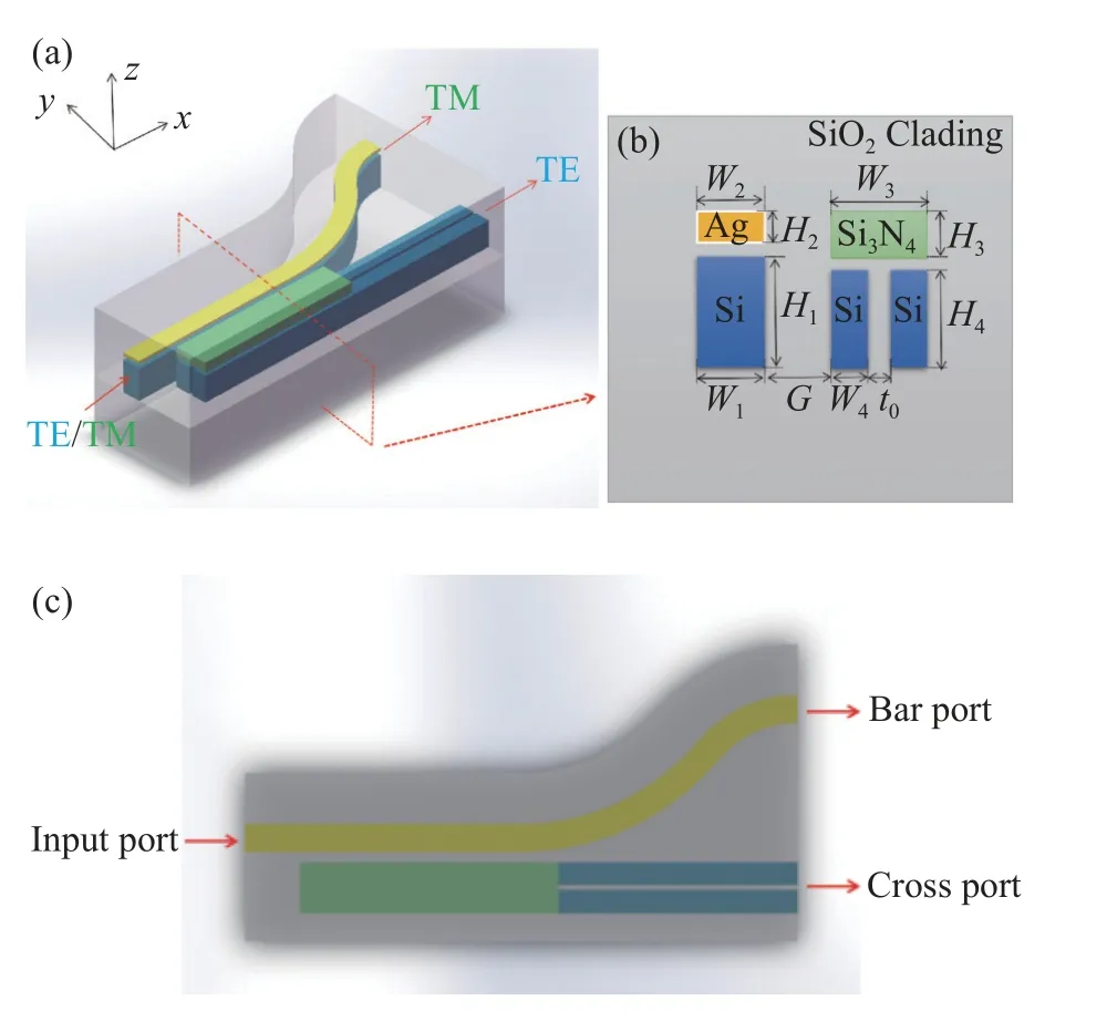
Fig.1 (a) 3D schematic diagram, (b) cross-section and(c) top-view of the proposed PBS device
To evaluate the polarization beam splitting performance of the PBS, typical indicators include bending radius (r1), coupling length (LC), operating wavelength (λ), waveguide spacing (G), the total length of the device (L1), insertion loss (IL) and extinction ratio (ER).
The extinction ratio (ER) of the PBS can be defined as[26]:

This work proposes a dual-slot ultra-compact PBS consisting of a hybrid plasma HSW and a silicon nitride hybrid VSW.The structural parameters of the HSW and VSW are optimized by using a mode analysis of FEM based COMSOL multi-physics.The HSW and VSW waveguides are arranged into non-uniform triangular grids according to their optical field characteristics.The PBS uses a physically-controlled triangular mesh throughout the domain with a minimum mesh size of 2 nm for input and output ports.The minimum mesh value of other computational domains is 5 nm, respectively.The scattering boundary condition is used, which reduces the reflected energy.
3 Mode characteristics
According to the phase matching conditions,the widths of the VSW and HSW (W2,W3) are optimally selected so that the effective refractive index real parts of the TE mode are equal.Then, the TE polarized light incident from the input port is effectively coupled to the adjacent VSW through the coupling region, while the TM polarized light is outputted from the bar port with almost no coupling.
As mentioned above, the widths of the VSW and HSW should only meet the phase-matching conditions of TE polarization and maximize the phase mismatch of TM polarization.It can be seen from Fig.2 (a) (color online) that the effective refractive index of the mode varies with the waveguide width.The widths of the VSW and HSW are optimized for phase matching between TE modes,while Re (neff) of the TE and TM modes increases gradually as the widths of the HSW and VSW (W2orW3) increase and while the increased rate of the TE mode is larger than that of the TM mode.The results show that when the HSW width and VSW width are 302 nm and 550 nm, the real part of the effective refractive index for the TE mode in the HSW and VSW satisfying the phase matching condition are 2.382 and 2.377, respectively.The effective refractive index of the TM mode is 2.46 and 2.72, indicating that there is a large phase mismatch of TM modes in the two waveguides.
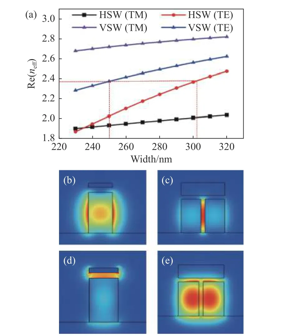
Fig.2 Influence of waveguide width on the effective refractive index.(a) The real part of the refractive index of TE mode and TM mode varying with width in the HSW and VSW; the field distribution of the TE mode in the (b) HSW and (c) VSW, and the field distribution of the TM mode in the (d) HSW and (e) VSW
The electric field profiles of dominant supermodes are held in the coupling region at a 1 550 nm working wavelength using the optimized structural parameter, as shown in Fig.2(b)-(e) (color online).For the TE and TM modes in the HSW and VSW,the distribution of the TE mode in the two waveguides is also very similar.
The supermodes are excited at corresponding arms when the polarized light enters the coupling region by satisfying the phase-matching condition.Henceforth, the required minimum length called the coupling length (Lc) is used to represent the coupling of the injected polarized beams from the input port to the cross port.It is an essential parameter to evaluate the compactness of the device.The selection of structural parameters plays a vital role in obtaining the minimumLcthat depends on effective index difference.In the proposed PBS, the phase matching criteria is planned only for TE mode.Hence,Lc[27-28]is expressed as
whereλrepresents the working wavelength, andnTE0andnTE1are the effective indices of TE polarized supermodes.The shorter coupling length (LC) is achieved for device compactness when the TE modes’ index difference is larger.For designing the proposed PBS,Gplays a significant role between the two arms, whereas the coupling length is also one ofG’s parametric functions, as shown in Fig.3.
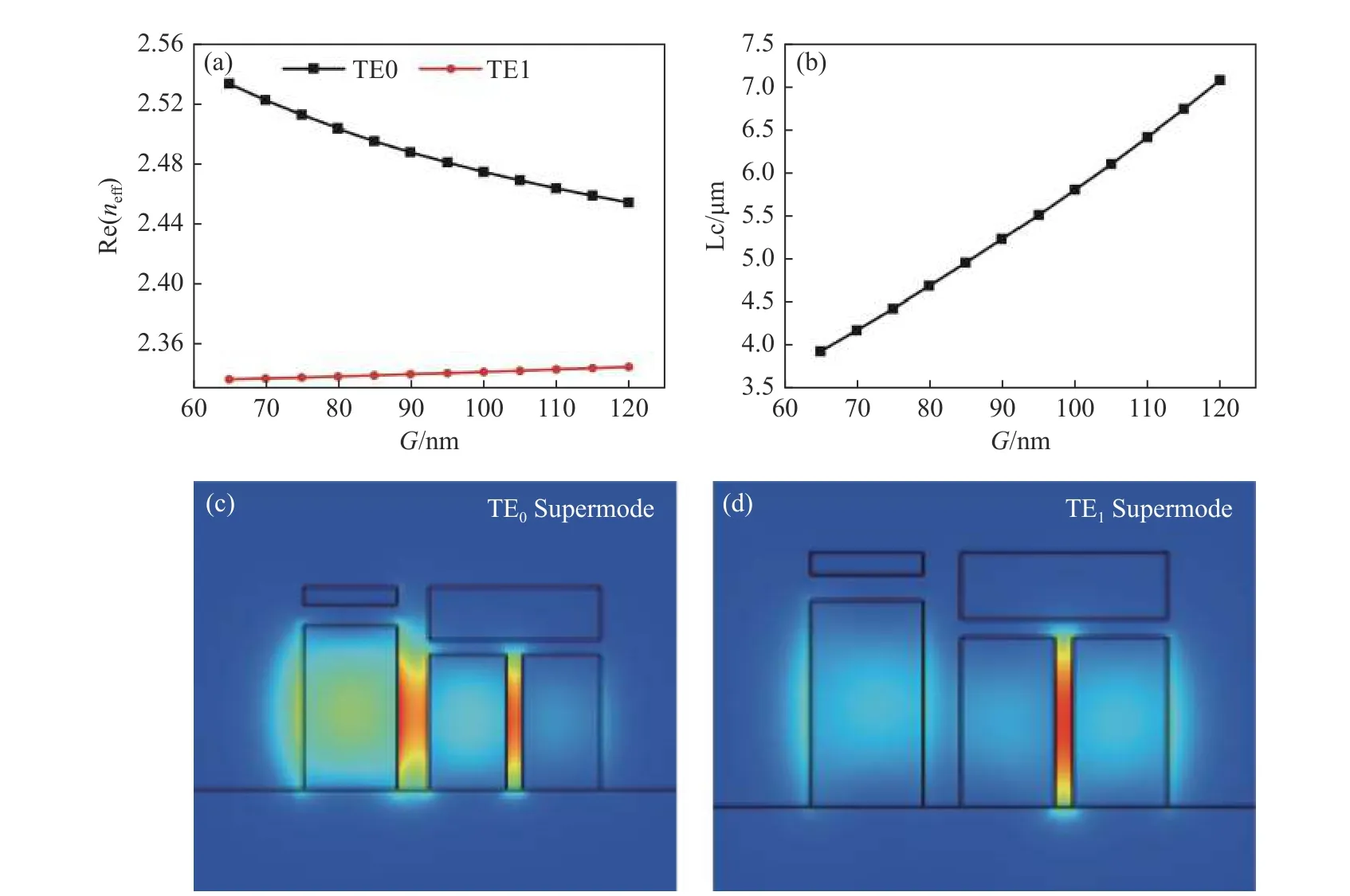
Fig.3 Effect of waveguide spacing G.The effect of G on (a) the effective refractive index and (b) the coupling length p.Electric field profile of supermodes at 90 nm of G, (c) TE0, and (d) TE1
When the distance between two waveguides in the coupling region is large, the mode optical signals are transmitted independently in their corresponding waveguides.At this time, there is no mode coupling between the parallel waveguides in the coupling region.The two parallel waveguides are close to each other and form a coupling system when the distance between the waveguides is close to the magnitude of the wavelength.Due to the action of the evanescent wave, the light signals of two adjacent parallel waveguides will be transformed into energy.When the waveguide meets the phase matching condition, the energy of the signal in the HSW waveguide can be completely converted to another waveguide by selecting the optimal coupling length.The HSW is equal to that of a mode in the coupled waveguide, which is to say that the phasematching condition is satisfied and the specific model in the coupled waveguide can be precisely excited.By selecting the optimized coupling length,the energy of the signal in the HSW can be completely converted to another waveguide.
4 Simulation results and discussions
To further study the polarization beam splitting characteristics of the PBS, several geometric parameters (waveguide spacingG, bending radiusr1, the total length of the deviceL1, operating wavelengthλ) are discussed.The influences of the waveguide dimension parameters onG,r1,L1, andλare studied as shown in Figs.4 ~ 6 (color online).Figs.4 ~ 6 show ER and IL at the bar and cross ports when the input light is the TE and TM modes,respectively.Here,W2=302 nm,W3=550 nm,H1=560 nm,H2=60 nm,H3=180 nm andH4=460 nm.
The influences ofGon ER and IL are shown in Fig.4 (color online).In Fig.4(a) and 4(b), ER in the TE mode first increases and then decreases with an increase ofG.The ER value increases from 30.35 dB to 31.79 dB and then decreases to 16.89 dB,while IL in the TE mode decreases first and then increase.ER of the TM mode first increased and then decreased with an increase ofG.The ER value increased from 22.6 dB to 35.9 dB and then decreased to 17.97 dB, while IL of the TM mode showed a decreasing trend.To reach a compromise between ER and IL,G=90 nm was selected.The coupling length (Lc) is identified by using the theoretical Eq.(5), the obtainedLcvalue for the proposed PBS is 5.2 μm whenG=90 nm.
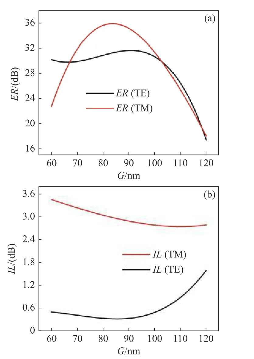
Fig.4 The influence of G on ER and IL at the cross and bar ports.Here, W2 = 302 nm, W3 = 550 nm, r1 =4 μm, λ=1.55 μm and G= 90 nm
The curved part is connected to the tail of the straight HSW to prevent the coupling of two adjacent waveguides.As can be seen from Fig.5 (a) and(b), ER in the TE mode and ER in the TM mode first increase and then decrease withL1, while IL in the TE mode and IL in the TM mode first decrease and then increase.To reach a compromise between ER and IL,L1=9 μm was chosen.
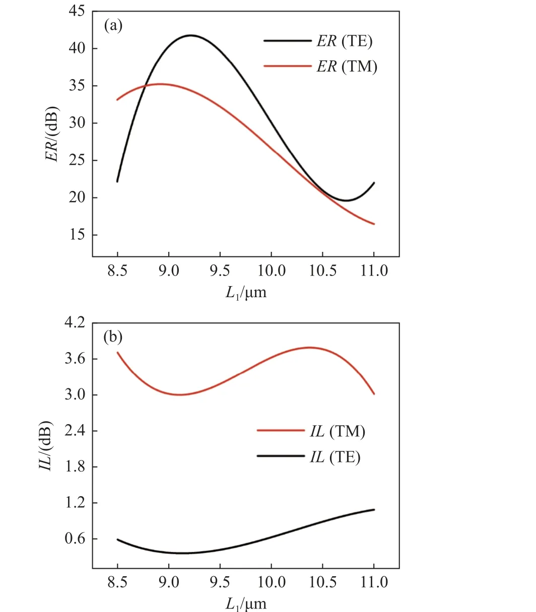
Fig.5 The influence of L1 on ER and IL at the cross and bar ports.Here, W2=302 nm, W3=550 nm, r1=4 μm,λ=1.55 μm and G= 90 nm
It can be seen from Fig.6 (a) and 6(b) that ER in the TE mode is greater than 27 dB and IL is less than 1.1 dB at the wavelength of 1 525~1 625 nm.ER of the TM mode was greater than 16 dB and IL was less than 4.2 dB.To reach a compromise between ER and IL, we chose the wavelengthλ=1 550 nm.The calculated PER value in both inputs of ER is high at the operating wavelength of 1 550 nm, and the ER value of the TE input(35.1 dB) is lower than the TM input (40.9 dB).
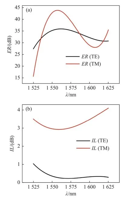
Fig.6 The influence of λ on ER and IL at the cross and bar ports.Here, W2=302 nm, W3=550 nm, r1=4 μm,λ=1.55 μm and G= 90 nm
Fig.7 (a) and 7(b) (color online) show the propagation for the TE and TM modes.When the TE mode is inputted at the input port, it is strongly coupled in the coupling region and finally outputted from the cross port.However, it can also be observed from Fig.7 (b) that when launching a TM mode, it will propagate along the HSW waveguide and directly output at the bar port.Therefore, the two modes are well separated.
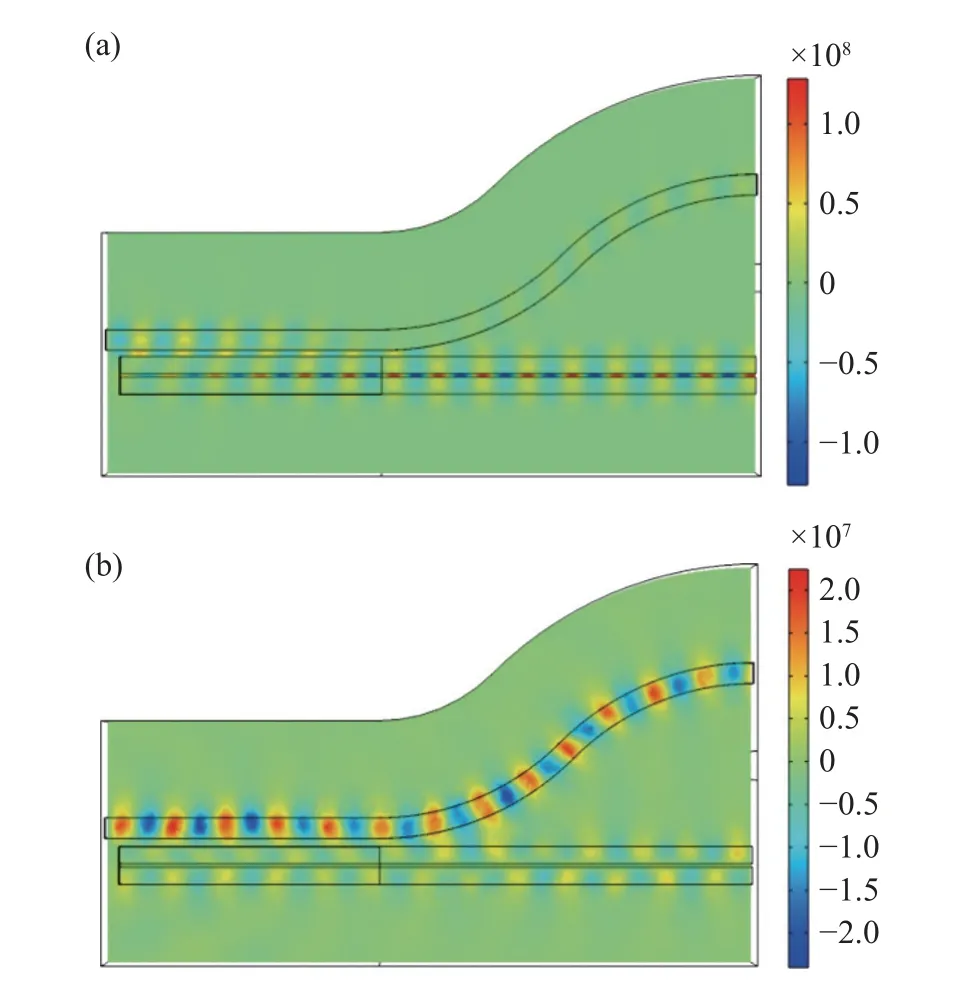
Fig.7 The light propagations in the designed PBS of the(a) TE-Ey, (b) TM-Ez
After the above discussion, it can be seen that whenL1=9 μm,r1=4 μm, andG=90 nm are selected, the PBS has the best performance, which is shown in Fig.8 (color online).Here, the length of the PBSL1=9 μm and the wavelength is 1 550 nm.As can be seen from Fig.8 (a) ~ 8(e), when TE polarized light in the HSW is emitted to the input port,the TE mode is mostly concentrated in the silicon layer of the HSW in section (c).In section (d), the TE mode is transmitted to the coupling region, and part of the waveguide is coupled from the HSW to the VSW.In section (e), almost all the light fields have been cross-coupled to the VSW.Similarly, it can be seen from Fig.9 when the TM polarization mode is inputted in the HSW.This is because the metal is sensitive to the TM mode in the HSW, and is not conducive to the standardized power of the TE mode.The ER and IL of the TE and TM modes were 35.1 dB, 40.9 dB, 0.34 dB, and 2.85 dB,respectively.In addition, the designed PBS has a bandwidth of 100 nm, which provides a promising platform for increasing communication capacity.
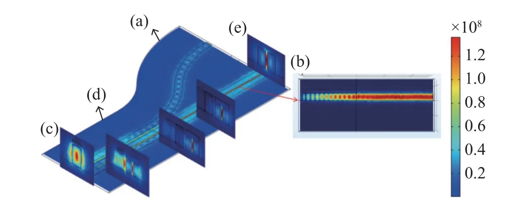
Fig.8 TE polarization beam splitting and electric field distribution at the corresponding position for the TE mode
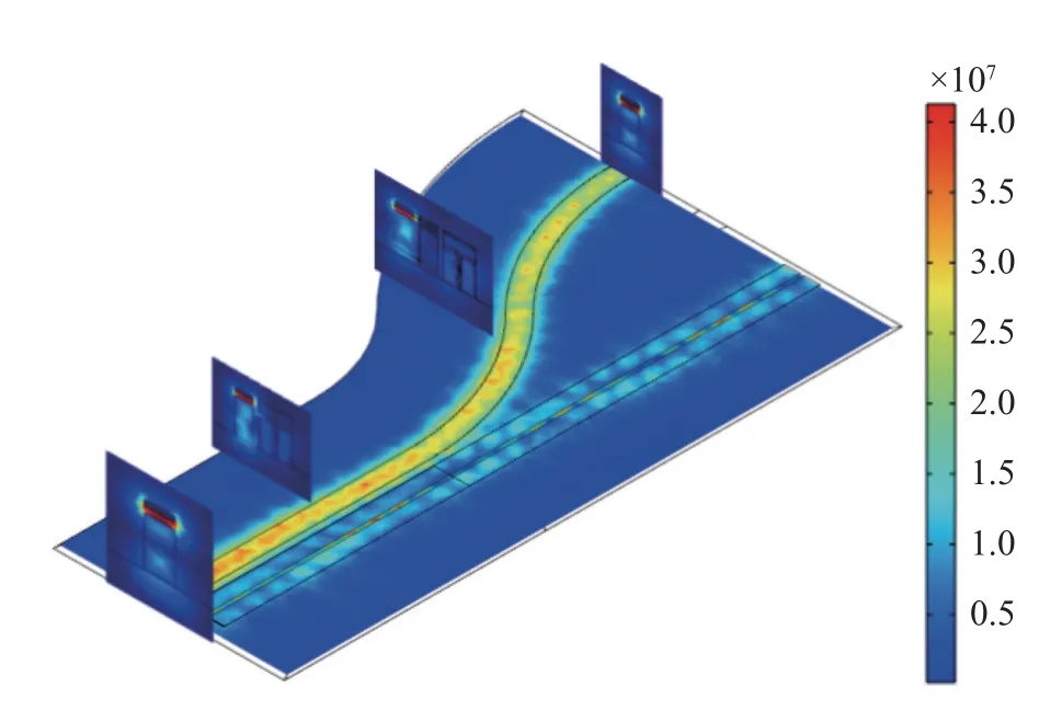
Fig.9 TM polarization beam splitting and electric field distribution at the corresponding position for the TM mode
A comparison of the designed PBS with other PBSs is shown in Table 1.PBS proposed in this paper has performed well compared with the references, as mentioned in the above table.For both polarizations of input, the IL and ER are much better than the existing works.
5 Proposed fabrication process and fabrication tolerances
In the experiment, the polarization beam splitter based on the asymmetric mixed plasma structure can be realized using the proposed manufacturing process, as shown in Fig.10 (color online).First, theSOI substrate is cleared and rotated and coated with a resist by using Electron Beam Lithography(EBL).Secondly, the pattern is transferred to the Si layer by Inductively Coupled Plasma (ICP) dry etching to realize the waveguide coupler.The Ag layer was deposited by vacuum evaporation to generate the HSW waveguide[36-37].The same approach implements the VSW waveguide.The Si3N4filmwas deposited by ICP Chemical Vapor Deposition(ICPCVD), scale resistance was removed by Plasma Enhanced Chemical Vapor Deposition (PECVD),and 2 μm thick SiO2cladding was deposited[38].
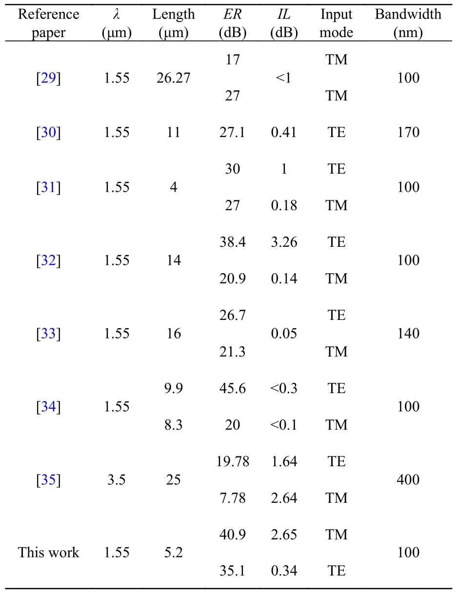
Tab.1 Performance comparison of the polarization

Fig.10 The fabrication process of the designed polarization beam splitter
The size deviation provides great reference value to manufacture a polarization beam splitter with a mixed plasma structure.The size of the HSW waveguide (W1,H1,H2) is analyzed, as shown in Figs.11 (a)-11 (c) (color online).In Fig.11 (a),ΔERand ΔILis less than 5.8 dB and 0.47 dB withW1in the range of 292 nm to 312 nm.Because the TE mode propagates in the Si layer, the Si thicknessH1has a great influence on TE mode transmission.In Fig.11 (b), withH1in the range of 550 nm to 570 nm, TE changes more than TM with the change ofH1.For the TE mode, ΔERis less than 8.7 dB,while for the TM mode, ΔERis less than 3.6 dB.H2is closely related to ohmic loss due to the Ag layer’s thickness.In Fig.11 (c),H2ranges from 50 nm to 70 nm.With the change ofH2, ΔILfor TE mode is less than 0.4 dB, while that for TM mode is less than 0.6 dB.
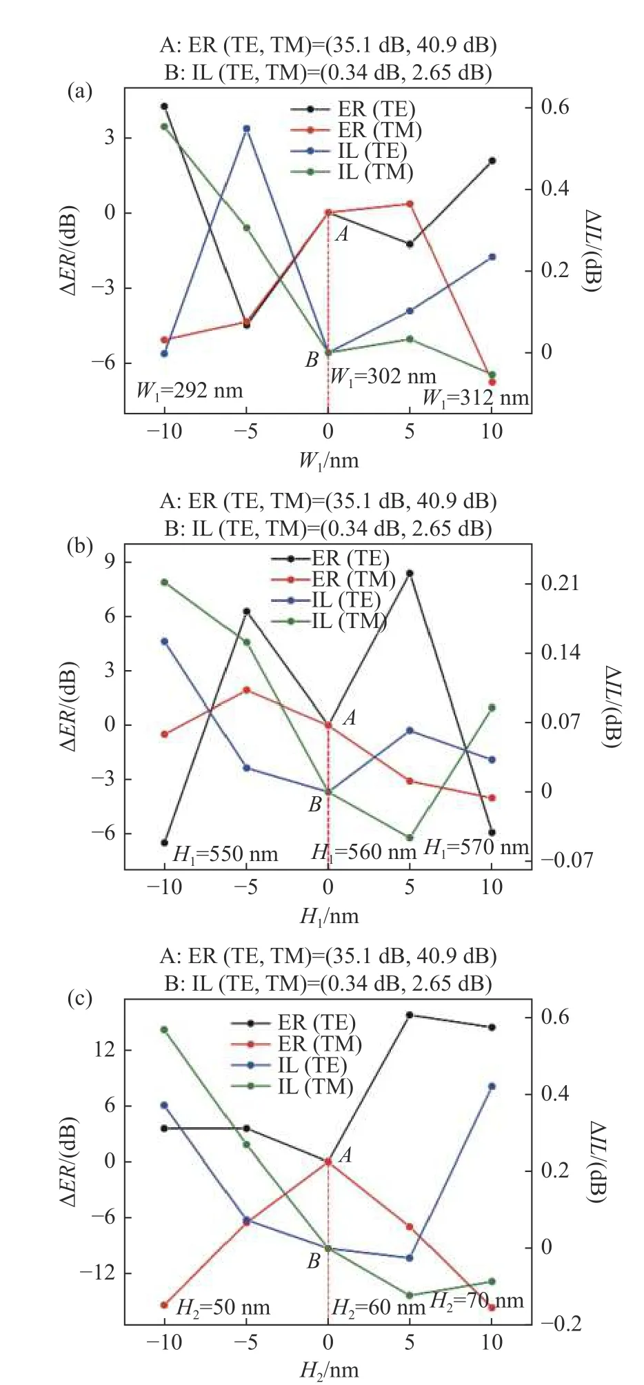
Fig.11 Effects of different dimensional tolerances on ER and IL.(a) W1=302 nm, (b) H1=560 m and (c)H2=60 nm
The dimensions of the VSW (H3,H4) are analyzed, as shown in Fig.12 (a) and (b) (color online).In Fig.12 (a),H3ranges from 170 nm to 190 nm.For the TE mode, ΔERis less than 2 dB and ΔILis less than 0.02 dB.For the TM mode, ΔERis less than 4.8 dB and ΔILis less than 0.04 dB.In the VSW, the TM mode mainly exists in the Si.In Fig.12 (b),H4varies from 450 nm to 470 nm, and the TE mode changes little withH4.For the TM mode, ΔILis less than 2.4 dB.
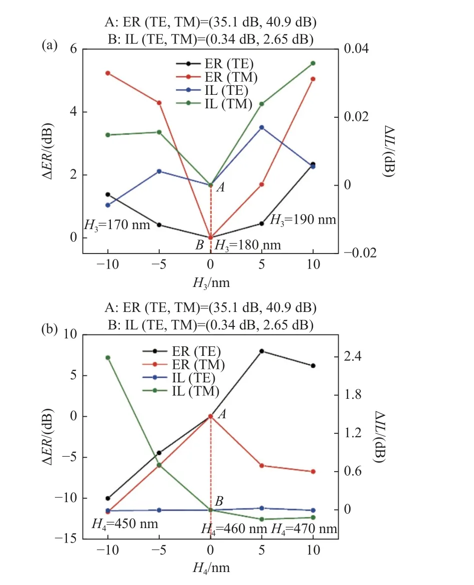
Fig.12 Effects of different dimensional tolerances on ER and IL.(a) H3=180 nm and (b) H4=460 m
6 Conclusion
In summary, a hybrid plasma HSW and silicon nitride hybrid VSW Polarization Beam Splitter(PBS) is proposed.According to the mode characteristics of the TM and TE modes at a 1.55 μm wavelength, the PBS is realized by phase matching the TE mode and phase mismatching the TM mode.By optimizing the parameters, ER and IL are 35.1 dB and 0.34 dB for the TE mode, 40.9 dB and 2.65 dB for the TM mode asW2= 302 nm,W3=550 nm,r1=4 μm,G=90 nm,L1=9 μm.At the same time, the PBS has a working bandwidth of 100 nm,providing a promising platform for improving communication capabilities.
