Design of all-optical half-adder based on nonlinear effect and linear interference effect
2023-10-07YANGJianyeWURongZHANGHaochen
YANG Jian-ye,WU Rong,ZHANG Hao-chen
(School of Electronic and Information Engineering, Lanzhou Jiaotong University,Lanzhou 730070, China)
* Corresponding author,E-mail: 1114332211@qq.com
Abstract: An all-optical half-adder is designed by combining the nonlinear effect and linear interference effect of photonic crystals.By dividing the light source into two parts equally, the half adder AND gate and XOR gate are designed separately.The nonlinear effect is used to realize the AND gate with high contrast,and the linear interference effect is used to realize the XOR logic, so that the overall response speed of the device is improved.In this design structure, the device only has threshold requirements for the signal light source power.When the signal power is greater than 51.4 mW/μm2, it has stable output and strong anti-interference ability.The designed contrast of the half adder carry output port is 20.69 dB, and the output port contrast is 20.13 dB.The data transfer rate is 0.75 Tbits/s and the occupied area is 623 μm2.
Key words: all-optical half adders; ring resonator; micro-cavity; optical logics; linear interference effect
1 Introduction
In recent years, due to the significant growth of communication bandwidth, the need for faster processors and optical fiber systems is becoming more and more urgent.The existing semiconductor devices affected by electronic speed is about to reach the bottleneck, and optical devices have high-speed processing characteristics, and are not susceptible to electromagnetic noise, so the use of optical devices in the future is foreseeable[1-3].
All-optical logic devices play an important role in optical signal processing such as addressing and optical computing[4].Currently, all-optical logic devices designed based on photonic crystals are popular among designers for their smaller footprint and low manufacturing cost.Photonic crystal is a kind of artificial material with periodic change of refractive index in space, which has two characteristics: photon band gap and photon locality[5-6].After the introduction of defects in the crystal[7-8], light wave transmission can be guided.The resulting defective photonic crystals are used in many optical devices, such as filters[9-10], wavelength division multiplexers[11-12], optical fibers[13-14], beam splitters[15-16], and optical logic devices[17-20].There are other applications of photonic crystals which should be addressed, such as sensors[21], solar cells[22], photodetectors[23], and etc.Many methods can be used to realize optical logic devices by photonic crystals, such as multi-mode interference[24], autocollimation transmission[25]and linear interference, etc.The optical logic devices designed by using linear interference effect and nonlinear effect have simple structure and are suitable for largescale integration.To achieve simple all-optical logic gate, designers often make use of linear interference effect, so that the designed devices have the advantages of simple structure and fast response.When the designed logic device has multiple outputs, it is not possible to obtain high-efficiency and high-contrast outputs only by means of linear interference, so the use of nonlinear materials is necessary.In order to remove the interference frequency signal and enhance the coupling efficiency of the output end, a filter structure can be added to the output end to select the frequency of the output light wave.Commonly used structures include micro cavity structure[26]and ring cavity structure[27].The filter frequency can be adjusted by setting the radius of the medium column.In 2020[28], Sani M Het al.designed an all-optical half-adder with an occupying area of 249.75 μm2by using nonlinear effects.Its logical contrast is high, the delay time is 3 ps,and four levels of input power are required to realize the logic function.In 2021[29], Chattopadhyay Tet al.proposed an all-optical half-adder and full-adder data processing circuit based on the nonlinear Mach-Zehnder interferometer switch.The structure is easy to expand and the intensity of the light source used is 10 W/μm2.In 2022[30], Saadi Ket al.implemented an all-optical half-adder logic gate based on the concept of linear interference of light waves, with a compact structure and a size of 17 μm×12.2 μm.
The all-optical half-adder designed in this paper is a new structure.It is combining nonlinear effect and linear interference effect.It can control the output by using the power of the light source and reduce the dependence on the power of the light source.
2 Theoretical basis
2.1 Nonlinear effect
The structure designed in this paper uses two identical nonlinear ring cavities.When the input light intensity changes, the refractive index of the nonlinear material changes, resulting in its resonant wavelength changes[31].The refractive indexes of many nonlinear materials depend on the light intensity, and its refractive index is expressed as follows:
where,n0is the weak-field refractive index, and the product factorn2is the nonlinear refractive index[32],indicating that the total refractive index increases with the increase of light intensityI.Assuming that the field is linearly polarized, the total polarizations caused by second and third order nonlinearities are:
χ(2)andχ(3)are second and third order nonlinear polarizabilities.Assuming that the nonlinear material has crystal symmetry, the second-order susceptibility can be ignored, so the nonlinear refractive indexn2is:
where Z0=376.7 Ω, is the free space impedance.The photonic crystal has two kinds of structure: air column and medium column.The air column is easy to manufacture and the medium column has the advantage of strong coupling.In this paper, a photonic crystal with a cubic lattice dielectric column structure is designed with lattice constanta=0.625 μm and filling factorr/a=0.18.The material of the dielectric column is Si with refractive indexn=3.46.The characteristics of the nonlinear annular cavity are explored through the structure of Fig.1(a) (color online), whereRis the nonlinear annular cavity and the nonlinear material set for the square shapedRin Fig.1(a) is doped glass, the radius is the same as that of a silicon dielectric column, which is 0.18a.The weak field refractive indexn0=1.4, and the nonlinear Kerr coefficientχ(3)=10-14m2/V2.The Gaussian light source is incident at IN and output at portsO1,O2, andO3.Fig.1(b) (color online), shows the normalized power curves of the three output ports when the light source is in the band of 1.52-1.58 μm.It can be seen that the light wave with wavelength of 1.55 μm is mainly output from theO2andO3ports after coupling through the ring cavity.Fig.2(color online) shows the influence of the light wave power on the output of Fig.1(a).The wavelength of the light source is 1.55 μm, and the refractive index of the nonlinear annular cavity is close to its linear refractive index when the light wave power is small[33-34].It can be seen from Fig.2(a) that the light wave is mainly output fromO2andO3.After the increase of light wave power, due to the increase of refractive index increment of nonlinear annular cavity[35], the coupling efficiency of light wave is greatly reduced.It can be seen from Fig.2(b) that light wave is mainly output fromO1terminal.

Fig.1 Characteristics of nonlinear annular cavity.(a) Structure of nonlinear annular cavity.(b) Normalized power of output port in the band of 1.52-1.58 μm

Fig.2 Normalized output port powers at (a) low power incidence and (b) high power incidence
2.2 Linear interference effect
When there is phase difference between two beams of the same path, there will be constructive or destructive interference.When the phase difference is 2mπ (m=0,1,2,3...), there will be constructive interference, the output signal will be enhanced.When the phase difference is (2m+1) π, there will be destructive interference, the output signal will be weakened.Fig.3(a) (color online) is an XOR gate structure, whereAandBare input terminals andOis out put[36].The wavelength of the used signal light source is 1.542 μm.When the input is logic '01' or '10',the output is logic '1', and when the input is '00' or'11', the output is logic '0'.Fig.3(b) (color online)shows the steady-state electric field diagram when both signal light sources are logical '1', light wave destructively interferes with each other at the output port, and the output is '0' when the input is logical'11'.

Fig.3 (a) XOR gate structure.(b) Steady state electric field diagram when input is logic '11'
3 Design and optimization
3.1 Structure and simulation results of half-adder
In computer data processing, the addition of binary numbers is one of the most basic arithmetic operations, which plays a crucial role in information processing.A half-adder can add two binary numbers, with two inputsAandB, and two outputs SUM=A⊕B, and CARRY=AB.Fig.4 (color online)shows the structure of the half-adder designed in this paper.The wavelength of the continuous light source is 1.542 μm and the power is 66.4 mW/μm2.After the light source enters from portsAandB, it will be divided into two parts and propagate along two paths at the same time.In order to ensure that the light source can enter the two paths equally, the two silicon dielectric columns at the coupling point DC1 and DC2 are adjusted and the radiusris set to 0.158 4 μm to enhance the light coupling to the right waveguide.After the light source enters from portA, most of the light waves along the waveguideW1andW2will be output along the input portBafter resonance.The same is true for the light waves along portB, so the influence on the two output terminals is weakened and the device has better performance.There are two nonlinear ring cavities on the left side of the half-adder structure.When there is no signal or only one signal input, the input power is low.As can be seen from the results of the structure in Fig.5(a) (color online), when the CARRY port has only a small power input, the output power is also small.When the two inputs are both logical'1', the optical path difference between the two input signals at the CARRY output end is the same.Due to the presence of constructive interference, the optical input power at the CARRY port increases,and the increase of the power will greatly change the refractive index of the nonlinear material, and the light wave will be output from the CARRY end.On the right side of the structure, by adjusting the optical path difference between the two input signals at the SUM output port, when the input is '11',the two signals destructive interference at the SUM output port presents, and there is only light wave output of very small power.When the input is '01' or'10', the SUM port has a high power output, and the XOR logic is realized.Fig.5 (color online) shows the normalized power curves of the CARRY and SUM output ports after signal input.The device has a high logical contrast.The contrast of the CARRY port is as high as 20.93 dB and that of the SUM port is 13.17 dB.
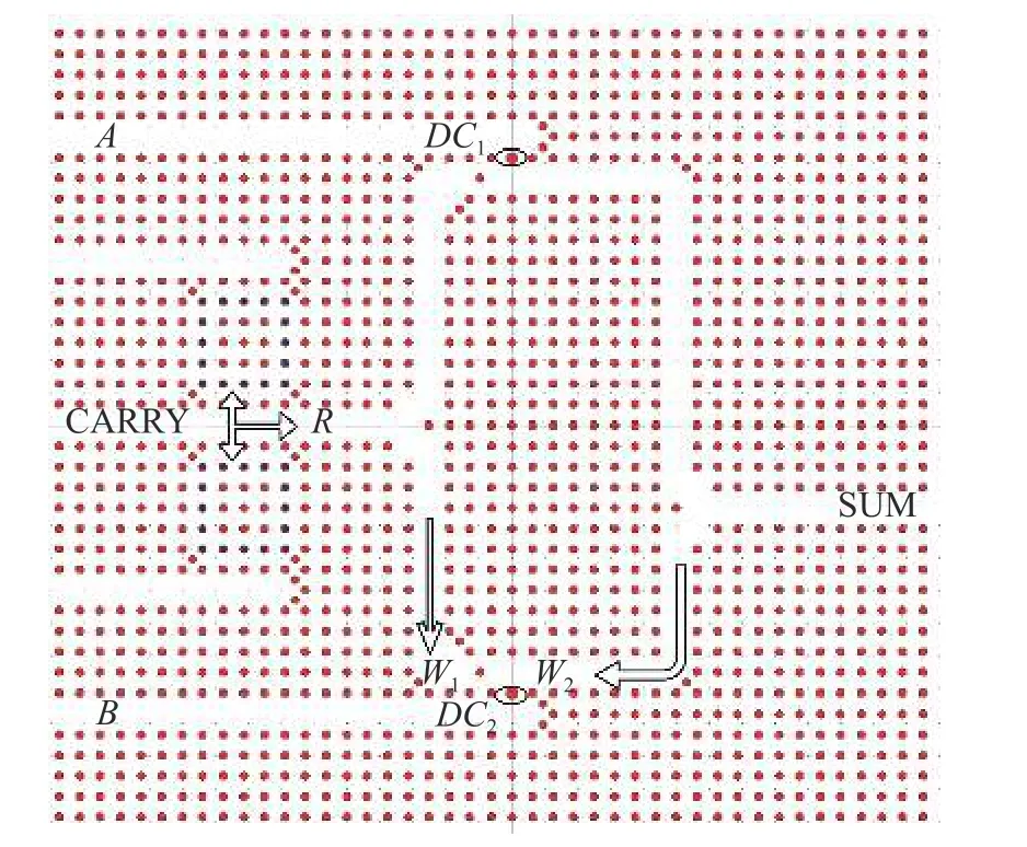
Fig.4 Half-adder structure

Fig.5 Half-adder normalized power output curve.(a) Input is logical '01'.(b) Input is logical '10'.(c) Input is logical '11'
3.2 Structure of the optimized half-adder and the simulation results
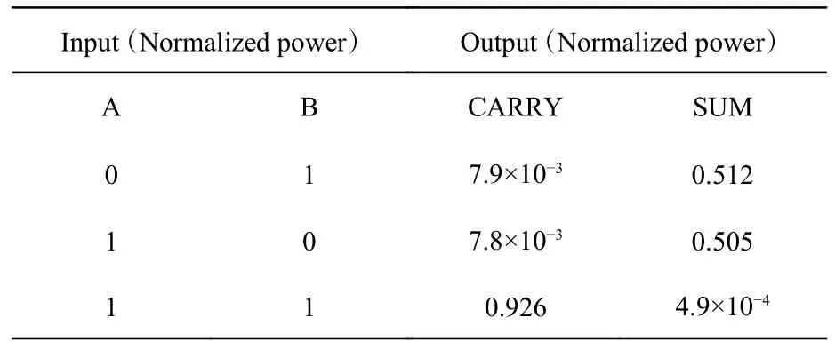
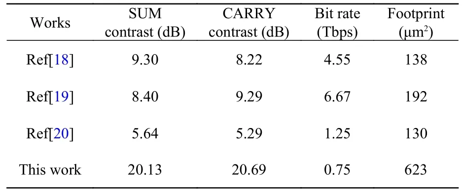
The above half-adder structure has high contrast, but low output power and small output power difference between logic '0' and '1'.After analysis, it is found that there are two reasons: one is that when the two signals are input, the rectangular waveguide leads to excessive reflection; the other is that as the signal enters the output waveguide without coupling structure, and the coupling efficiency is low.In order to increase the output efficiency of logic '1' of CARRY and SUM ports, a micro-cavity coupling structure is added to the output port, and a dielectric column is added to the rectangular waveguide to reduce the loss, and the SUM output port is adjusted.The structure of the improved half-adder is shown in Fig.6 (color online),MC1andMC2are two microcavity structures with a medium column radius of 0.158 4 μm in the middle.After optimizing the structure of the half-adder, the power of the signal light source is adjusted to 169.9 mW/μm2.Fig.7(color online) shows the steady-state diagram of electric field when the input signal logic is '01', '10'and '11' respectively.Fig.8 (color online) shows the normalized power curve of the output ports after the structure improvement.It can be seen that the normalized output powers of the logic '1' of CARRY and SUM ports have been greatly improved.Table 1 shows the improved performance parameters of the half-adder.The designed structure has a data transmission rate of 0.75 Tbits/s and occupies an area of 623 μm2.The above parameters of our proposed structure are listed in Table 2 and compared with some previous structures.
Tab.1 The output parameters of the latter half-adder
Tab.2 Summarized features of proposed structure and previous works
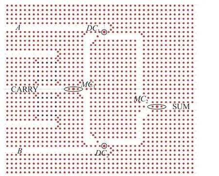
Fig.6 Optimized half-adder structure

Fig.7 Steady state diagram of half-adder electric field.(a) Input is logical '01'.(b) Input is logical '10'.(c) Input is logical '11'

Fig.8 Normalized power output curve.(a) Input is logical '01'.(b) Input is logical '10'.(c) Input is logical '11'
3.3 Influence of light source power on device performance
The stability of the device is a problem that we are very concerned about.For the nonlinear device,a higher power of the light source is desired.The stable output of the power of the light source is related to whether the correct logic output can be obtained.In this paper, the input light source is divided into two parts, so that AND gate and XOR gate can be designed separately.The nonlinear effect plays a crucial role in the design of the AND gate, while the influence on the XOR gate is very small, so the requirement for the light source is greatly reduced.In Fig 9 (color online), the influence of the power of the light source on the output of the device under different logic inputs is analyzed, which can be obtained from Fig 9(a).When the power of the signal light source is greater than 51.4 mW/μm2, there is a better contrast of the AND gate and a higher normalized output power.As can be seen from Fig.9(b), the output of XOR gate is extremely stable and basically does not change with the power of the light source, which is a characteristic of the design based on linear interference effect.The power of the signal light source can be roughly divided into two phases.When the power is less than 51.4 mW/μm2, the device cannot work, and when the power is greater than 51.4 mW/μm2, the device has better logic function.
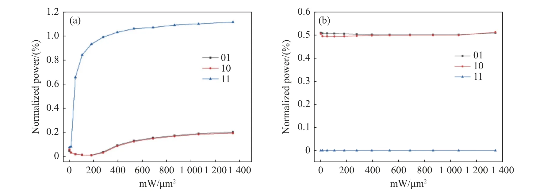
Fig.9 Influence of light source power on output.(a) Impact on CARRY output.(b) Impact on SUM output
4 Conclusion
This paper presents and designs a one-bit alloptical half-adder which combines nonlinear effect and linear interference effect.There are two nonlinear circular cavities in the structure, which are controlled by the total optical power of the two input signals.The simulation results show that when the light source power is 169.9 mW/μm2, the contrast ratio of CARRY and AND output ports is greater than 20 dB, and the data transfer speed is 0.75 Tbps.When the input power is greater than 51.4 mW/μm2,the structure can realize the logic function well.
