First-principles study of non-radiative carrier capture by defects at amorphous-SiO2/Si(100)interface
2023-09-05HaoranZhu祝浩然WeifengXie谢伟锋XinLiu刘欣YangLiu刘杨JinliZhang张金利andXuZuo左旭
Haoran Zhu(祝浩然), Weifeng Xie(谢伟锋), Xin Liu(刘欣), Yang Liu(刘杨),Jinli Zhang(张金利), and Xu Zuo(左旭),4,5,†
1College of Electronic Information and Optical Engineering,Nankai University,Tianjin 300350,China
2Institute of Electronic Engineering,China Academy of Engineering Physics,Mianyang 621999,China
3Microsystem and Terahertz Research Center,China Academy of Engineering Physics,Chengdu 610200,China
4Key Laboratory of Photoelectronic Thin Film Devices and Technology of Tianjin,Nankai University,Tianjin 300350,China
5Engineering Research Center of Thin Film Optoelectronics Technology,Ministry of Education,Nankai University,Tianjin 300350,China
Keywords: interface defect,carrier capture coefficients
1.Introduction
Around the world, silicon dioxide (SiO2) is a common component of sands.In microelectronic systems, amorphous silicon dioxide(a-SiO2)is used as an insulating layer.Charge capture by defects in the SiO2and transition layers is a critical problem that must be addressed in order to improve semiconductor device dependability.Unlike defects in bulk a-SiO2,when defects capture charge carriers at the interface of a-SiO2and Si (a-SiO2/Si), it will be difficult to recover electric neutrality,causing device performance to deteriorate and eventually leading to device failure.[1–4]Unsaturated dangling bonds,also known asPb-type defects found at the a-SiO2/Si interface are the major electronically active defects,are located in the interface of a-SiO2/Si and are detected using the electron spin-resonance(ESR)spectroscopy[5–8].ThePbdefect is discovered at a-SiO2/Si(111), with its isolated sp3hybrid dangling bond oriented in the (111) direction, orthogonal to the interface[5].Other two unique defects,Pb0andPb1,which are situated in the technologically important(100)interface,with isolated sp3hybrid dangling bonds pointing in the directions of (111) and (211), respectively.[2,8]Because the capture and accumulation of carriers to these defects cause the gate voltage to change and acts as non-radiative recombination sites to diminish the minority carrier density,understanding the microscopic mechanism of carrier capture and identifying dominant defects is crucial.[9,10]Unlike point defects in a-SiO2, interface traps seldom anneal at ambient temperature and continue to interfere with device function.[9]
Because direct measurement of the carriers capture process is challenging experimentally,especially in terms of identifying relevant defects, it is vital to investigate the related phenomena using theoretical calculations based on anab initiotechnique.[11,12]The adiabatic approximation,[13]Marcus theory,[14]quantum charge transfer theory[15]and static coupling theory[16–18]have been used to construct the electron–phonon coupling matrix, which determines the carriers capture properties of defects.Recently,Alkauskaset al.[18]established a method for calculating the electron–phonon coupling matrix using a one-dimensional(1D)configuration coordinate for the effective vibrational wave function and static coupling theory.This theory was applied to many hole capture defects in GaN and ZnO, and the hole capture coefficients found are consistent with experiment data.Therefore, in our work, we investigate the non-radiative carrier capture coefficients of thePb0andPb1defects using this 1D static coupling theory.Our results indicate that thePb0andPb1defects form positive centers more easily than negatively charged defect centers, and are indeed non-radiative recombination center in the interface of a-SiO2/Si(100).
2.Theoretical method
The spin-polarized first-principles calculations are performed in the Viennaab initiosimulation package (VASP)[19,20]with projector-augmented-wave (PAW)pseudopotentials.[21]Generalized gradient approximation(GGA) in the Perdew–Burke–Ernzerhof (PBE) form[22,23]is used for the optimization of geometrical structure and a cutoff energy of 500 eV for the plane-wave expansion is adopted.The convergence criteria are 10−5eV and 0.01 eV·˚A−1for energy and force, respectively.The structure models ofPb0andPb1defects are obtained by Liet al.,[24]with a dimension of 15.4 ˚A×15.4 ˚A×35.0 ˚A.Hybrid functional based on the Heyd–Scuseria–Ernzerhof (HSE06) method[25]is employed to obtain the exact electronic properties.
The formation energy(Ef)of defectXin charge stateqis calculated by
Theorris the change in electrostatic energy from the periodic boundary condition (Eperiodic) to the open boundary condition(Eisolated)for an isolated defect with chargeq[27]
where the last term is an alignment term of the classical electrostatic calculation to that of the DFT calculation.[28]
The finite element method is employed to correct the formation energy, and the charge density and dielectric constant profile of interface defects are extracted from the first principles calculations.[24]The defect charge is approximated by a Gaussian distribution.The Gaussian distribution is defined for the periodic boundary condition as[27]
whereσis the standard deviation, which defines the localization of the defect wave function,Q0= 1.6×10⁻¹⁹C is the elementary charge, andqis the charge of the defect.The uniform background charge density ofqQ0/Ωis added to obtain better convergence under the periodic boundary condition,andΩis the volume of the simulation unit cell.Under the ground boundary condition and without the uniform charge background,Eq.(3)can be written as
The permittivity profile can be obtained by polarizabilities of atoms, which include the electronic polarizabilities(αelec) and the ionic polarizabilities (αion).[29]The static permittivity can be written as
where polarizabilitiesαelecandαionof Si atoms in different oxidation states can be obtained in Ref.[29].A normalized Gaussian smearing function is multiplied to each atomic effective polarizability to smooth the permittivity profile.Thus,the permittivity profile along thez-axis is defined as
whereαec+αnis the polarizability of thei-th Si atom at thez-positionzi,and the standard deviationσis chosen to be 1.4 ˚A, which is the distance between two adjacent Si planes along the [001] direction, and the permittivity profile can be found in Ref.[24].
武成龙和鬼算盘打得异常激烈。回龙剑如银蛇飞舞,不断攻击着鬼算盘的全身,然而鬼算盘那二尺一寸长的、近尺宽的、怪异的、乌黑发亮的铁算盘好像一面盾牌一样有效扼制了长剑的攻势。长剑的轻灵飘逸与铁算盘的沉重而笨拙相映成趣,不时响起“叮!叮!叮!”轻脆悦耳的碰撞声,如果没有斗场中刺耳的剔肉刮骨声掺杂其间,会让人感到那不是一场生死搏杀,而是一场陶醉人心的表演。
The electrostatic potentialV(r) is the solution of the Poisson equation ∇·[ε(r)∇V(r)] =−ρ(r), and the electrostatic energiesEperiodicandEisolatedare calculated by solvingE=(1/2)V(r)ρ(r)drfor the corresponding model electrostatic potentialV(r)under the respective boundary condition.It should be noted that theEisolatedis obtained by scaling the simulation box uniformly.
Thus,the+/0 and 0/−charge-state transition levels calculated from the formation energy of Eq.(1)are given by
The relevant calculation results can be found in the supporting information.
Non-radiative carrier capture via multiphonon emission is a common phenomenon for deep defect levels in semiconductors.As shown in Fig.1, the initial excited state of the defect vibrates around the equilibrium geometry.Owing to the electron–phonon coupling, the deformation of the structure will change the electronic state of the defect and form final ground state.Then,the final ground state will relax to the equilibrium structure due to phonon–phonon interactions,and the atomic relaxations are represented by a 1D configuration coordinateQ,the minima of the two potential energy surfaces are offset vertically by ∆E, which corresponds to the chargestate transition level, and horizontally by effective configuration coordinate ∆Qbetween the excited state and the ground state.According to the 1D static coupling theory, the corresponding capture coefficient is given by Alkauskaset al.[18]
whereVis the volume of the supercell, and it will replace byS(the surface areas of the a-SiO2/Si(100))because we are concerned with interface defects.gis the degeneracy factor(for a-SiO2/Si(100),g=1).W2ifis the elertron–phonon coupling matrix elements of initial and final states,ξimandξfnare the vibrational wave function of initial excited state with vibrational frequencyωiand final ground state with vibrational frequencyωf, respectively, the vibrational frequency can be obtained by solving the 1D Schr¨odinger equation for potential energy surfaces around the equilibrium geometry.ωmis the thermal occupation number of the initial excited vibrational stateξim,which determines the temperature-dependence of the capture coefficient,and ∆Ecorresponds to the energy of charge-state transition with respect to the VBM for hole capture and CBM for electron capture.

Fig.1.Schematic of configuration coordinate for non-radiative carrier capture.The red and blue lines represent initial excited state with vibrational wave function ξim and final ground state with vibrational wave function ξfn,respectively.∆E is the ionization energy of the defect,∆Eb serves as a classic energy barrier of carrier capture,and Q is 1D effective configuration coordinate.
The degree of deformation is described by the 1D effective configuration coordinate ∆Qof initial and final states
wheremαand ∆Rαtare the mass and the displacement along the directiontfrom the equilibrium atomic coordinate of atomα,respectively.
The rationality of 1D static coupling theory is premised on Huang–Rhys factorS ≫1,which corresponds to the large lattice relaxation associated with the change of the charge state,thus it is possible to replace the sum over all vibrational degrees of freedom with one special phonon model.[30]TheSis defined as
3.Results and discussion
3.1.Geometric structures and electronic properties of Pb0 and Pb1 defects
The concentration of thePb0defect in the a-SiO2/Si(100)interface is approximately 5×1012cm−2,[32]located in the second Si layer near the interface.ThePb0defect is constructed primarily by removing a Si atom from the second layer of the interface on the Si side,resulting in four dangling bonds,three of which are saturated by H atoms,and the fourth dangling bond is thePb0defect(Fig.2(a)).In the case of thePb1defect,which is located in the topmost layer of the Si side,thePb1defect concentration in the a-SiO2/Si(100) interface is around 1×1012cm−2,[32]which is a fifth of thePb0defect concentration but nevertheless significant.Three different models have been proposed to define thePb1defect, including dimer, bridge and asymmetrically oxidized dimer (AOD)models.[32]The AOD model is the most likely candidate than the dimer and bridge models for thePb1defect, because the full set of hyperfine parameters is found to agree closely with the experimental data,[24,31]so we only choose this model in our research to study the carrier capture properties ofPb1defect.In the AOD model, the two lower back bonds of the fully coordinated Si atom near the SiO2layer are oxidized(Fig.2(b)).Due to the existence of dangling bonds,the neutralPb0andPb1defects have a magnetic moment of 1µB.

Fig.2.The geometric structure of neutral (left) and positively charged(right)(a)Pb0 defect and(b)Pb1 defect.

Fig.3.The geometric structure of neutral (left) and negatively charged(right)(a)Pb0 defect and(b)Pb1 defect.
Table 1 shows the bond lengths and bond angles of the Si atom containing a dangling bond (Si0) and the other three Si atoms coordinated to Si0at defect centers.When the defect captures a hole, the unpaired electron of the dangling bond along with the magnetic moment vanishes, and the defect structure tends to a plane structure similar to that of sp2hybridization (Fig.2), resulting in shorter Si–Si bonds and larger ∠Si–Si–Si bond angles.However, for thePb1defect,the bond length of the Si atom connecting to the three O atoms(Si3O) and Si0becomes longer due to the higher electronegativity of the O atom, which makes the type of bonding between O and Si between covalent and ionic bonds,resulting in different properties of Si3O.In terms of electron capture, the dangling bond’s unpaired electron would pair, and the magnetic moment would vanish, while Si–Si bond lengths would lengthen and ∠Si–Si–Si bond angles would decrease(Fig.3).And the relaxation of Si0contributes the most to ∆Q, which can be found in the percentage of ∆QSi0in the ∆Q(Table 1).
The energy levels of thePb0andPb1defects before and after hole (electron) capture are all determined by examining the density of states(DOS),as shown in Fig.4.The Si0atom contributes the most to the defect energy level,when the neutral defect captures a hole(electron),the magnetic moment becomes zero due to the unpaired electron in the dangling bond would vanish(pair).

Table 1.The change of Si–Si bond lengths,∠Si–Si–Si bond angles and mass-weighted distortions of Si atom with a dangling bond ∆QSi0 and all atoms ∆Q for Pb0 and Pb1 defects by capturing hole or electron.
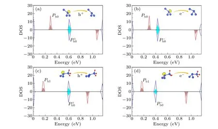
Fig.4.Spin-polarized local density of state (LDOS) of Pb0 defects (a) by capturing a hole and (b) by capturing an electron, Pb1 defects(c)by capturing a hole and(d)by capturing an electron.The red and blue lines represent defect levels before and after hole(electron)capture,respectively.The brown and cyan regions represent DOS projection to Si atom with a dangling bond.The energy level of valence-band maximum(VBM)is set to 0 eV.
3.2.The carrier capture properties for Pb0 defect and Pb1 defect
ThePb0andPb1defects are amphoteric defects, which act as both a donor and an acceptor state in the bandgap of Si.The complete non-radiative recombination is a sequence of electron-hole pair capture processes.Associated with the(+/0) transition level, there are two capture processes: hole(p) capture for the neutral state () and electron (n) capture for the positively charged state().Similarly,there are also two capture processes involved in the (0/−) transition level:electron capture for the neutral state()and hole capture for the negatively charged state().The 1D configuration coordinate diagram is used to analyze the capture processes.The relative parameters to describe the temperature dependence of carrier capture coefficients are shown in Table 1.
For thePb0defect,the(+/0)and(0/−)transition levels are 0.26 eV and 0.79 eV above the VBM(i.e.,∆Eare 0.26 eV and 0.38 in hole and electron capture for neutral state,respectively), respectively, which accords with the experimental results that the defect levels of thePb0defect are broadly distributed with(+/0)transition level approximately 1/3 eV below the middle of the band gap and the(0/−)transition level approximately 1/3 eV above the middle of the band gap.[4]Figure 5(a)shows the configuration coordinate diagram for the transition betweenPb0andP,the equilibrium configuration ofPandPb0correspond toQ=0 andQ=∆Q,respectively.The energy barriers of hole capture (∆) and electron capture (∆E) are 5.34 meV and 199.53 meV, respectively, ∆is much smaller than ∆,indicating that the hole capture process for the neutral state is faster than the electron capture process for the positively charged state and smaller temperature dependence of carrier capture coefficient.Figure 5(b) shows the similar results for the transition betweenPb0and, the energy barriers ∆and ∆are 0.52 meV and 230.14 meV,respectively, indicating that the electron capture process for the neutral state is also faster than the hole capture process for the negatively charged state.
The carrier capture coefficients as a function of temperature are depicted in Fig.5(c), which includes the electron–phonon coupling and the overlap of potential energy surfaces.And the total non-radiative carrier capture coefficient (Ctot)under steady-state conditions[33–35]can be derived as


Fig.5.Calculated 1D confgiuration coordinate diagrams for the transition between(a)Pb0 and P,(b)Pb0 and P.(c)Non-radiative capture coefficients of Pb0 defect as a function of reciprocal temperature.

Fig.6.Calculated 1D confgiuration coordinate diagrams for the transition between(a)Pb1 and ,(b)Pb1 and .(c)Non-radiative capture coefficients of Pb1 defect as a function of reciprocal temperature.
4.Conclusion
In summary, we use first principles calculations and the 1D static coupling approach to investigate the carrier capture properties ofPb0andPb1defects,the existence of initial dangling bonds,making these defects to capture holes or electrons easily to eliminate the dangling bonds.Because of the bigger hole capture coefficients for neutral states,thePb0andPb1defects have a stronger capacity to capture holes than electrons,and the large non-radiative recombination coefficient further indicates that these defects are the non-radiative recombination center.The present study further demonstrates how reducing the formation and suppressing the activity of these defects will be key to maintaining device performance in the future.
Acknowledgments
Project supported by the Science Challenge Project(Grant No.TZ2016003-1-105), Tianjin Natural Science Fundation (Grant No.20JCZDJC00750), and the Fundamental Research Funds for the Central Universities, Nankai University(Grant Nos.63211107 and 63201182).
猜你喜欢
杂志排行

Chinese Physics B的其它文章
- First-principles calculations of high pressure and temperature properties of Fe7C3
- Monte Carlo calculation of the exposure of Chinese female astronauts to earth’s trapped radiation on board the Chinese Space Station
- Optimization of communication topology for persistent formation in case of communication faults
- Energy conversion materials for the space solar power station
- Stability of connected and automated vehicles platoon considering communications failures
- Lightweight and highly robust memristor-based hybrid neural networks for electroencephalogram signal processing