Narrowed Si0.7Ge0.3 channel FinFET with subthreshold swing of 64 mV/Dec using cyclic self-limited oxidation and removal process
2023-09-05HaoYanLiu刘昊炎YongLiangLi李永亮andWenWuWang王文武
Hao-Yan Liu(刘昊炎), Yong-Liang Li(李永亮),†, and Wen-Wu Wang(王文武)
1Integrated Circuit Advanced Process Center,Institute of Microelectronics,Chinese Academy of Science,Beijing 100029,China
2University of Chinese Academy of Sciences(UCAS),Beijing 100049,China
Keywords: Si0.7Ge0.3,FinFET,cyclic wet treatment,self-limited oxidation
1.Introduction
The demand for integrated circuits (ICs) with higher speed and lower power consumption has aroused great interest in technologies that provide higher mobility and better gate control capability in the channels of metal–oxide–semiconductor field-effect transistors (MOSFETs).[1]The present mainstream fin field-effect transistor (FinFET) technology, which was introduced to overcome limitations of planer technology, is facing serious scaling challenges beyond the 5-nm node.[2–4]To improve electrostatic integrity,the adoption of nanowire (NW) or nanosheet (NS) GAA device structure is expected to be necessary for shorter gate length in the future node.[5–7]Although GAA device with compatible processes is a natural extension of FinFET,it still requires some disruptive technological breakthroughs before mass production, such as inner spacer, S/D epitaxial grown, multiple Vt.[8–10]Meanwhile,SiGe high mobility channel FinFET has also been proposed as a promising candidate to replace Si Fin-FET due to its higher hole mobility,better negative bias temperature instability (NBTI) reliability than Si.[11]Moreover,the scaling of fin width to improve gate controllability and the increasing of fin height to improve driven capacity have been critical factors of FinFET devices.Therefore,the scaling of fin width of SiGe channel with high mobility needs further study,because there are relatively few relevant studies so far.
In this work, a narrowed Si0.7Ge0.3FinFET device with an excellent subthreshold slope(SS)of 64 mV/dec is demonstrated by employing a precise cyclic wet treatment process,which is based on a self-limited oxidation in each cycle.More importantly, compared with the conventional Si0.7Ge0.3Fin-FET, this narrowed Si0.7Ge0.3channel FinFET can realize a strong gate control capability.
2.Experiment
The key fabrication steps of narrowed Si0.7Ge0.3channel FinFET are presented in Fig.1.After a standardized Nwell formation,Si0.7Ge0.3film was epitaxially grown on an Si substrate via a reduced pressure chemical vapor epitaxial deposition (ASM Epsilon 2000).Then, Si substrate/Si0.7Ge0.3fin structure was patterned through the sidewall image transfer method under an optimized HBr/O2based plasma.Subsequently,shallow trench isolation(STI)filling and planarization were implemented, followed by a low-temperature STI densification annealing of 850◦C for 30 s.Then, Si0.7Ge0.3fin was revealed by using a 1:100 diluted HF solution.After a conventional Si0.7Ge0.3fin was prepared,a low-temperature SiO2deposition and dummy gate patterning were carried out.Afterwards,lightly doped drain(LDD)and source/drain(S/D)implantation with B and BF2dopant were implemented after spacer 1 and spacer 2 have been fixed.A low-temperature dopant activation of 850◦C for 30 s was performed to maintain the Si0.7Ge0.3fin stability.After dummy gate removal,nitric acid (HNO3) and hydrofluoric acid (HF) were separately used as oxidant and oxide remover agent to perform cyclic wet etching treatment on the exposed Si0.7Ge0.3fin.After several cycles of self-limited oxidation and removal process were implemented,the narrowed Si0.7Ge0.3fin with precisely controlled fin width was achieved.Afterwards,in-situO3passivation combined with Al2O3/HfO2bilayer high-kdielectric(HK)and TiN-based metal gate(MG)was employed to form the gate stack by using an atomic-layer-deposition tool.Finally,the standard Si FinFET processing was adopted to complete the narrowed Si0.7Ge0.3FinFET device fabrication.
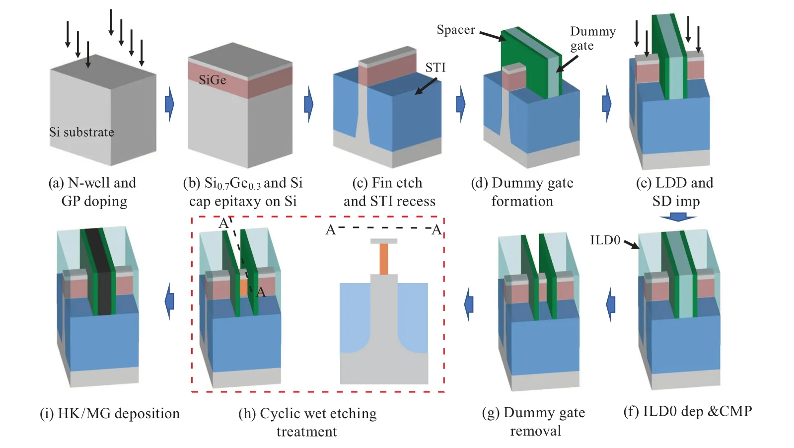
Fig.1.Key process of narrowed Si0.7Ge0.3 channel FinFET.
3.Results and discussion
3.1.Conventional Si0.7Ge0.3 fin preparation
Epitaxially grown quality and fin etching profile of SiGe film are two key factors for the conventional SiGe fin structure.Figure 2(a)presents theω–2θHRXRD scan result of epitaxial grow of SiGe on Si substrate, showing well-defined interference sub-peaks (Kiessig frings) on both sides of SiGe peak,which are characteristics of high-quality SiGe film.Meanwhile, the fitting result shows that the thickness of SiGe film is 29.58 nm and the percentage of Ge atoms is 31.83%.Figure 2(b)shows the result of Si0.7Ge0.3fin reveal after HBr/O2based plasma etching and STI recess.It is found that a completely vertical and uniform profile of Si substrate/Si0.7Ge0.3fin with a width of∼20.5 nm is attained.
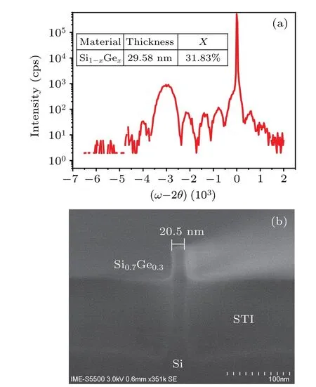
Fig.2.(a)HRXRD spectra result on epitaxially grown SiGe.(b)SEM image of Si0.7Ge0.3 fin post fin reveal.
3.2.Narrowed Si0.7Ge0.3 fin preparation
It was reported that SiGe film is completely etched off by using HF/oxidizer based solutions, such as HF:HNO3:CH3COOH and HF:H2O2:CH3COOH, to release the channel of Si GAA device[12,13]However, these mixed solutions cannot be directly applied to the narrowing of Si0.7Ge0.3fin, because the oxidation of Si0.7Ge0.3fin and its removal occur at the same time,and the width of Si0.7Ge0.3fin cannot be precisely controlled.
To precisely control the width of the narrowed Si0.7Ge0.3fin,a novel cyclic wet treatment process is proposed,in which oxidant for self-limited oxidation and oxide remover agent are used separately.In our experiment, 40% HNO3solution is selected for self-limited oxidation and 1% HF solution is selected for oxide removal.It is found that the oxidation of Si0.7Ge0.3fin can reach saturation when the immersion time of HNO3is longer than or equal to 40 s,and 0.63-nm Si0.7Ge0.3fin/per side can be accurately removed in the following HF solution when its etching time is larger than 5 s as shown in Fig.3(a).Therefore, self-limited oxidation with 40% HNO3solution for 40 s and this oxidation removal process with 1%HF solution for 10 s is chosen as the optimal process condition.Based on this cyclic wet treatment of self-limited oxidation/removal process, the precise control of Si0.7Ge0.3fin width can be achieved by controlling the number of cycles.Figure 3(b)shows the SEM result of Si0.7Ge0.3fin after 10 cycles of wet treatment post fin reveal.Comparing with Fig.2(b),the width of Si0.7Ge0.3fin is significantly narrowed with a high selectivity to Si cap layer.Meanwhile,it can also be seen that the Si0.7Ge0.3fin height can be well maintained in this newly developed process due to the high selectivity to Si cap.
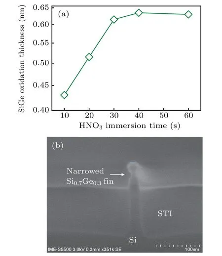
Fig.3.(a) Si0.7Ge0.3 fin removal thickness/per side in each cycle,(b)SEM image of Si0.7Ge0.3 fin after 10 cycles of wet treatment.
Figure 4 shows the mechanism of precise cyclic wet treatment process of the Si0.7Ge0.3fin.The oxidation characteristics of SiGe and Si in HNO3solution are different.For Si material, a stable and very thin SiOxlayer can be formed on its surface.However,SiOxand GeOxare simultaneously formed on the SiGe surface and the GeOxwill be dissolved in water,so the oxidation will not stop until sufficient SiOxis formed.[14,15]Therefore,one cycle of self-limited oxidation is completed before this oxidation has been completely removed by the HF solution.This signature is consistent with the phenomenon that oxidation thickness of Si0.7Ge0.3fin first increases and then turns saturated as HNO3solution immersion time going by.Therefore,a narrowed Si0.7Ge0.3fin can be precisely achieved by controlling the number of wet treatment cycles.
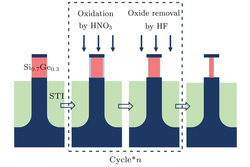
Fig.4.Mechanism of precise cyclic wet treatment process of Si0.7Ge0.3 fin.
3.3.Narrowed Si0.7Ge0.3 FinFET device
This newly developed cyclic wet treatment process is successfully applied to the preparation of the narrowed Si0.7Ge0.3FinFET.Comparing with the conventional Si0.7Ge0.3Fin-FET integration process,the main difference of this narrowed Si0.7Ge0.3FinFET is that this cyclic wet treatment process is inserted after the removal of dummy gate.More importantly,the HNO3solution or HF solution in this cyclic wet treatment process has sufficient selectivity to Si and other films(such as SiN spacers).Therefore, this cyclic wet treatment process is completely compatible with mainstream FinFET technology.
Figure 5 shows the EDS mapping analysis results of this narrowed Si0.7Ge0.3fin under the HK/MG stack at the end of fabrication process.It is found that the width of Si0.7Ge0.3fin is narrowed from 20 nm to 8 nm and the width of Si cap is almost unchanged.These results further confirm that this newly developed wet treatment process can accurately control the width of Si0.7Ge0.3fin and has a high selectivity to Si.Moreover,the multilayer HK/MG is well wrapped around the narrowed Si0.7Ge0.3fin, which may help to achieve an excellent gate controllability of this narrowed Si0.7Ge0.3FinFET.In addition, after cyclic wet treatment, it is also found that the surface of Si0.7Ge0.3fin is slightly concaved,which may have some influence on the performance of FinFET, such as gate control capacity.This slightly concaved Si0.7Ge0.3fin profile can be further improved by developing new dry etching in the future.
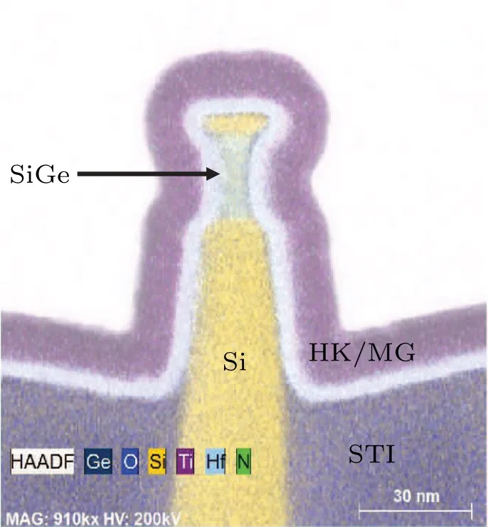
Fig.5.EDX mapping analysis result of narrowed Si0.7Ge0.3 FinFET device.
TheIDS–VGScurve of this narrowed Si0.7Ge0.3FinFET is given in Fig.6.IDSof 421µA/µm underVDS=VGS=−0.8 V,ION/IOFFratio of∼3×10⁵,and SS of 64 mV/dec are obtained.Comparing with the conventional Si0.7Ge0.3FinFET with optimized electrical performance reported earlier,[16]its SS can be reduced by 24%, improving from 87 mV/dec to 64 mV/dec.These mentioned results indicate that a stronger gate control capability to the Si0.7Ge0.3channel is attained after adopting a narrowed Si0.7Ge0.3fin by utilizing a precise cyclic wet treatment process.
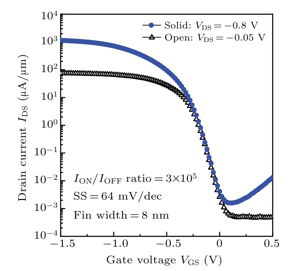
Fig.6.Transfer characteristics of narrowed Si0.7Ge0.3 FinFET.
The key electrical property of the narrowed Si0.7Ge0.3FinFET is compared with those of some reported SiGe FinFET/GAA devices.[3,17–23]Figure 7 summarizes the SSION/IOFFbenchmark of the reported SiGe FinFET/GAA devices.TheION/IOFFratio of the narrowed Si0.7Ge0.3FinFET is higher than the average value of the comparison groups.Its SS is the smallest in SiGe FinFETs and comparable to that of the SiGe GAA device.This result proves that the cyclic wet treatment after dummy gate removal is a promising technology to further improve the gate control of Si0.7Ge0.3FinFET.In addition,this novel wet treatment process can also provide a potential solution for realizing SiGe fins with different widths on the same wafer after introducing an additional mask.
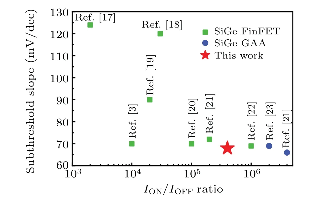
Fig.7.The SS–ION/IOFF benchmarks with reported SiGe FinFET/GAA devices.
4.Conclusions
In this work, a narrowed Si0.7Ge0.3FinFET device with a stronger gate control capability is presented by utilizing a precise cyclic wet treatment process,which is based on a selflimited oxidation and removal technology in each cycle.This cyclic wet treatment after dummy gate removal is a promising technology to further enhance the gate control of Si0.7Ge0.3FinFET.
Acknowledgement
Project supported by the Beijing Municipal Natural Science Foundation,China(Grant No.4202078).
猜你喜欢
杂志排行
Chinese Physics B的其它文章
- First-principles calculations of high pressure and temperature properties of Fe7C3
- Monte Carlo calculation of the exposure of Chinese female astronauts to earth’s trapped radiation on board the Chinese Space Station
- Optimization of communication topology for persistent formation in case of communication faults
- Energy conversion materials for the space solar power station
- Stability of connected and automated vehicles platoon considering communications failures
- Lightweight and highly robust memristor-based hybrid neural networks for electroencephalogram signal processing
