High‑precision high‑voltage detuning system for HIAF‑SRing electron target
2023-07-11KaiMingYanMingRuiLiYunBinZhouXiaoMingMaJinBinShangguanZhongKuiHuangXiaoJunWangMeiTangTangJieGaoHouKeHuangDaQinGaoLiJunMao
Kai‑Ming Yan ·Ming‑Rui Li ·Yun‑Bin Zhou ·Xiao‑Ming Ma ·Jin‑Bin Shangguan ·Zhong‑Kui Huang ·Xiao‑Jun Wang ·Mei‑Tang Tang ·Jie Gao ·Hou‑Ke Huang ·Da‑Qin Gao ·Li‑Jun Mao
Abstract The development of a detuning system for the precision control of electron energy is a major challenge when electron targets are used in ion-storage rings.Thus, a high-precision, high-voltage, detuning system was developed for the electron target of a high-intensity heavy-ion accelerator facility-spectrometer ring (HIAF-SRing) to produce accurate electron–ion relative energies during experiments.The system consists of auxiliary, and high-voltage detuning power supplies.The front stage of the auxiliary power supply adopts an LCC resonant converter operating in the soft-switching state and an LC filter for a sinusoidal waveform output in the post-stage.The detuning power supply is a high-voltage pulse amplifier (HVPA) connected with a high-voltage DC (HVDC) module in series.In this paper, the design and development of the detuning system are described in detail, and the test bench is presented.The test results demonstrated that the detuning system conforms to the technical specifications of the dielectronic recombination (DR) experiment.Finally, a Fe15+ DR spectrum was measured using the detuning system.The experimental data demonstrated a good experimental resolution and verified the reliability and feasibility of the design.
Keywords Detuning system ·Storage ring ·Dielectronic recombination
1 Introduction
More than 95% of the visible matter in the universe is in the plasma state; controllable nuclear fusion, which is a clean energy source contributing to the future of mankind,also occurs in the plasma environment.Therefore, understanding the properties and behavior of plasma is critical.Dielectronic recombination (DR) is one of the most fundamental electron–ion recombination mechanisms in various plasmas, which significantly affects the ionization balance and population levels therein.The recombination rate coefficient obtained in DR experiments can also be used to evaluate the environmental parameters (e.g., temperature and density) of plasmas and as benchmark data to test relevant theoretical methods and codes [1, 2].In addition, DR plays an important role in fundamental research and has been used to study the Quantum Electrodynamics(QED) effects on few-electron ions [3, 4], isotope shifts[5], hyperfine quenching [6], and hyperfine splitting [7].In recent decades, a series of DR experiments with High Charge Ions (HCIs) have been conducted at various storage rings, such as the test storage ring (TSR) at Max Planck Institute for Nuclear Physics (MPIK) in Heidelberg [8], the experimental storage ring (ESR) at GSI in Darmstadt [9],and the CRYRING at Manne Siegbahn Laboratory (MSL)in Stockholm [10]; the CRYRING has recently been relocated to GSI, and the CRYRING@ESR has served as a high-resolution DR experimental spectrometer.Currently,DR experiments in storage rings are performed using the electron beam provided by the electron cooler as the target.This method requires periodic detuning of the electron beam energy to obtain the expected relative energy between the electron and ion beams in the center-of-mass(cm) frame.During the detuning interval, the electron energy must return to the cooling point to maintain the quality of the stored ion beams.The problems associated with this method include the fact that the duty cycle for the detuning process in the measurement cycles is approximately 1/10th, which significantly reduce the efficiency of the experiment; therefore, the method is only suitable for DR measurements in the low-energy range.Currently,a new project, the high-intensity heavy-ion accelerator facility (HIAF), is under construction in China.The HIAF program aims to expand nuclear physics and related cutting-edge research into new areas.It comprises the following five components: a superconducting electroncyclotron-resonance ion source (SECR), superconducting ion linac accelerator (iLinac), booster ring (BRing),high-energy fragment separator (HFRS), and spectrometer ring (SRing) [11].The SRing at the HIAF can provide the experimental platform for atomic and nuclear physics [12,13].The SRing is equipped with an electron cooler and an individual electron target, which allows for performing precision DR spectroscopy for highly charged ions in a large energy range.The electron target is operated at an arbitrary energy level while the ion beam is continuously cooled by the electron cooler.Thus, SRing significantly improves the efficiency of the experimental measurements.Simultaneously, by changing the working point HV of the electron target, a significantly broader scan range of the electron energy can be available, thus achieving precise DR spectroscopy measurements in a higher energy range.The schematics of the HIAF-SRing construction and the working method of the DR experiment are shown in Fig.1.The electron cooling area and target are located in the long and short straight sections of the SRing, respectively.The operation of the electron target in the DR experiments can be described as follows: Initially, the working energy of the electron target is set to coincide with the energy of the electron cooling point.Energy scans are performed to measure the DR process at low collision-energy levels.The working energy is then changed step-by-step to measure the DR process at high CM collision energy levels.Furthermore, the deceleration of highly charged ions is possible in the SRing, which is beneficial for DR measurements over a large CM collision energy range.
The key technology required for an electron target is the development of a fast electron energy detuning system,which is used to produce accurate electron–ion relative energies in experiments.To verify the DR experimental scheme of the SRing, a high-precision, high-voltage detuning system is designed and developed for the electron target of the SRing; it can output adjustable millisecond pulses that float at a high DC voltage, as shown in Fig.2.A bias voltage of up to −10 kV is provided by a high-voltage DC (HVDC)module.This was used to set the working energies, as shown in Fig.1.A high-voltage pulse amplifier (HVPA) connected in series to the HVDC module can provide a precise detuning voltage.The maximum detuning voltage is 1 kV with a minimum voltage step of 1 V.The ripple of the detuning voltage is required to be less than 100 ppm to obtain an accurate electron–ion relative energy for detuning.The rise/fall times must be less than 500 μs for a 1 kV detuning voltage to avoid changing the ion energy owing to the cooling drag force.The pulse width is in the range of 5–20 ms, depending on the recombination rate.A demonstration experiment was conducted with a detuning system in a cooling storage ring(CSR), a heavy ion accelerator, at the Institute of Modern Physics.This study describes the development, characteristics, and performance of a high-precision high-voltage detuning system.In addition, good experimental test results were obtained, which substantiated the accuracy of the proposed detuning system technology scheme and provided a reliable technical solution for the HIAF electron target detuning system.
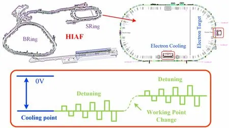
Fig.1 (Color online) Schematic diagram of the HIAF-SRing construction and working method of the DR experiment

Fig.2 The DR experiment requires the waveform of the output of the detuning system

Fig.3 Connection scheme between the gun and detuning system
2 Structure and connection of detuning system
The electron gun of the target (ET gun) was connected to a detuning system, which also represents a significant capacitive load.The ET gun consists of a cathode, grid,anode, and filament, as shown in Fig.3.Electrodes were used to extract electrons from the thermionic cathode.The cathode was directly connected to the output of the detuning system.The other electrodes were connected to three individual DC power supplies, which floated on the detuning system.The main parameters of all the power supplies used for the Fe15+demonstration experiment are listed in Table 1.

Table 1 Main parameters of all the power supplies for the electron gun and collector
3 High‑precision of high‑voltage detuning system
The use of a low-frequency isolation power supply produces low-frequency conduction and radiation interference, which are difficult to eradicate or shield.This will significantly affect the control setting, which needs to reach the reference voltage on a microvolt scale, and the overall detuning system, which needs to limit the ripple voltage level to below 100 ppm.Switching noise can be minimized by using the soft-switching state in the discontinuous conduction mode (DCM), whereas the highfrequency sinusoidal waveform can provide low-harmonic power transmission.Therefore, the main auxiliary power supply incorporated the front-stage LCC resonant converter operating in the soft-switching state and the LC filter used in the post-stage for providing a high-frequency sinusoidal power transmission.This power supply structure, in addition to providing a low-switching noise and low-harmonic high-frequency isolation voltage for all the power supplies of the ET-gun, also provides an effective resistance when the system power supply is rapidly energized (equivalent open circuit), or the electron beam trajectory distortion (equivalent short circuit).
Including the HVPA and HVDC modules in the detuning system is the key to producing a detuning waveform.The detuning power supply of this system adopted the structure of the HVPA and HVDC modules in series.The unique properties of the HVPA allow it to drive the four-quadrant voltage and current required by the capacitive load of the ET gun, whereas the mature HVDC module can ensure a constant output of the DC high-voltage power for electron cooling.An overview of the high-precision high-voltage detuning system is presented in Fig.4.In this section, the design process of the main auxiliary power supply and highvoltage detuning power supply of the high-precision, highvoltage detuning system is introduced in detail.
3.1 Main auxiliary power supply
The zero-current soft-switching states of insulated gate bipolar transistors (IGBTs) can be achieved when the LCC converter operates in the DCM, which effectively reduces the interference noise caused by the hard-switching process.The switching frequency of IGBTs must be less than 2 times the resonant frequency [14].The LCC resonant square-wave voltage output uses an LC filter to form a double-resonant frequency point on the logarithmic frequency curve.By designing the appropriate resonance and filter parameters and the voltage clamping capacitor determined by the detuning load characteristics,the main auxiliary power supply can output a high-frequency sinusoidal waveform with a constant-amplitude voltage.The structures of the front-stage resonance converter and the poststage filter are shown in Fig.4.
A transfer function was established for the front-stage LCC resonance converter and post-stage filter.The doubleresonance frequency point can be obtained by assuming that the imaginary part of the transfer function is zero.According to the structure of the front-stage resonance converter and the post-stage filter shown in Fig.4, the imaginary part transfer function of Eq.(1) is as follows:
The parametersa,c, andeare described in the appendix.
The filter resonant frequencyf1and DCM resonant frequencyf2can be obtained by solving (1).Equations (2) and(3) are the approximate solutions:
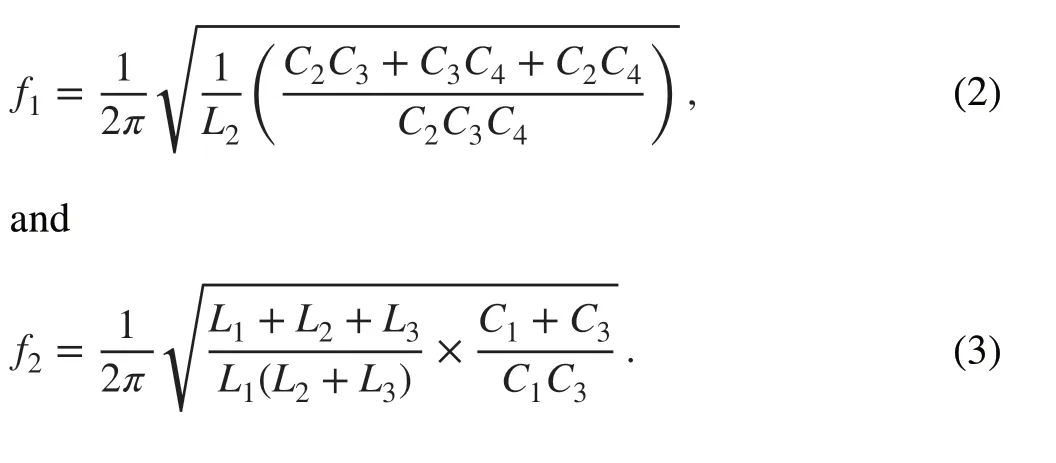

Fig.4 An overview of the high-precision, high-voltage detuning system
Simplifying the post-stage filter and load of the main auxiliary power supply facilitates the analysis of the complex structure of the main auxiliary power supply.The post-stage filter and load are equivalent to the impedanceZload, and the load current is equivalent to a constant in the switching period [15, 16].Under steady-state conditions, a closed-form solution can be deduced from the state equations by analyzing the resonance converter and filter structure using the state-space method [16].
The converter is determined to operate in state 1 by assessing the same polarity of the parallel resonant capacitor voltageVC3and the supply voltageVAB; otherwise, the converter operates in state 2.The angle of state 1 is set asθ1, and the angle of state 2 is set asθ2.When the next switch is triggered, state 1 ends and the output capacitor voltageVC3changes its polarity, converting it to state 2.Consequently,the end of one state is the beginning of another state, and the switching of states continuously results in the change of the polarity of the capacitor voltageVC3.The two different state relationships betweenVC3andVABin the DCM are shown in Fig.5.Based on the aforementioned analysis, the voltage of the parallel resonant capacitor is zero when the state polarity is switched, which can be expressed by Eqs.(4), (5), and(6) as follows:
and
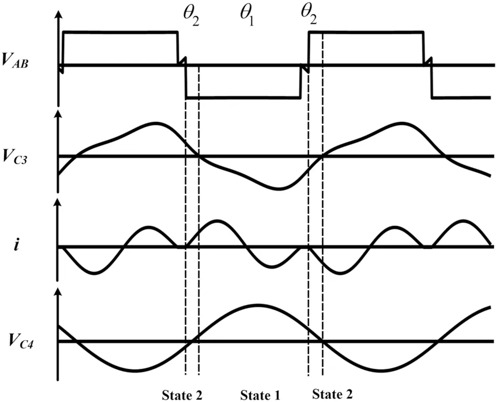
Fig.5 Relationship between VC3 and VAB in the DCM for the two different states
The state equation can be used to solve theθ2value of state 2 in theVC3polarity switching process, as shown in Eqs.(7) and (8), wheret1andt2are the durations of states 1 and 2, respectively, and A and B are the coefficient matrices of the resonance converter and filter structure [14].Matrix A describes the internal behavior of the resonance converter and filter structure.Matrix B represents the relationship between the external condition, resonance converter, and filter structure.

The formulas for calculatingφ1,φ2,andφ3are shown in the appendix.
The turn-off time range of the switch and the time of the LCC resonant current passing 0 V need to be further calculated using theθ2.
Using the formula above, an LCC high-frequency series–parallel resonant sinusoidal power supply with a switching frequency of 22 kHz was designed.The design parameters of the LCC series–parallel resonant sinusoidal power supply are summarized in Table 2.Figure 6 presents the logarithmic frequency curves of the double-resonant frequency point obtained with the designed converter under different equivalent system loads.Figure 6 reveals that the voltage decay factor of the third-harmonic wave, or any harmonic above the third wave, remains unchanged in the process of different load changes of the designed converter, which maintains the sinusoidal output of the power supply within a certain load range.
3.2 High‑voltage detuning power supply
The high-voltage-detuning power supply was an HVPA connected in series to an HVDC module, which uses a special control method.The overall structure of the detuningpower supply and its feedback control methods are illustrated in Fig.7.The external extended high-precision 24-bit DAC controlled by the Zynq FPGA (Field Programmable Gate Array) controller provides a reference voltage(Vref_HVPA+Vref_HVDC) to theA1shown in Fig.7.This reference voltage is compared with the overall feedback voltage measured by the high-precision high-voltage divider so that PI feedback control of the entire detuning power supply is achieved through a loop control.The control setting (Vref_HV_DC) of the HVDC module was achieved using a separate photoelectric conversion control.The advantage of the detuning power supply control method is that the voltage of the ET-gun load can be quickly and dynamically compensated by the HVPA four-quadrant output.The load voltage can accurately return to the high-voltage DC initial value set by the HVDC module after the end of each detuning pulse despite being affected by the parasitic parameters in the system and the capacitive load characteristics of the ET gun.

Table 2 Design parameters and specifications of the LCC resonant sinusoidal power supply
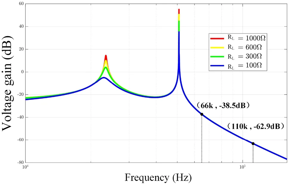
Fig.6 (Color online) Logarithmic-frequency curves of the double resonance points for the different equivalent loads
The series structure of the detuning power supply causes the output pulse current of the HVDC module to be consistent with that of the HVPA during the detuning process.Therefore, a parallel pulse capacitor between the HVDC module output terminal and the HVPA output terminal as a current bypass is necessary.This structure effectively protects the HVDC and filters the output voltage of the HVDC module to reduce the overall output ripple of the detuning power supply.
HVPA uses multiple MOSFET (Metal Oxide Semiconductor Field Effect Transistor) and Darlington transistors in series to achieve positive and negative symmetrical cascade structures [17].The multiple-MOSFET improved the overall withstanding voltage.A strict high-voltage equalization protection circuit must be designed for each MOSFET.The special structural design of the symmetrical cascade can rapidly drive the capacitive load of the ET gun to the falling edge of the end of the positive pulse or to the rising edge of the end of the negative pulse.In the static state, the symmetrical cascade assumes the function of high-voltage equalization, whereas in the dynamic state,the symmetrical cascade must be used as an AC circuit for a high-voltage linear output.Therefore, it is necessary to supply each MOSFET device with a sufficient driving voltage and establish the correct working state to ensure the stability of symmetrical cascades in static and dynamic operations.The load capacitance and ET structure capacitance are equivalent to 5 nF, and the instantaneous driving current of the 1 kV high-voltage output may rise as high as 10 mA, In which case the instantaneous driving current needs to be achieved by designing reasonableCHandCLfront-stage energy storage capacitors for the frontstage ± 2 kV high-voltage power supply at the ends of the symmetrical cascade.
A linear optocoupler was used to isolate the high-voltage potential between the weak current control voltage and the Darlington transistor base electrode, which not only produces a linear transmission of the weak current control signal but also safely drives the Darlington transistor base electrode to operate in the linear amplification range.A current-series negative feedback circuit was designed between the error output and the optocoupler input to increase the optocoupler input impedance and stabilize the drive current.A voltage parallel negative feedback circuit is designed between the optocoupler output and the Darlington transistor base electrode, which performs the I–V conversion on the drive signal output by the linear optocoupler while further regulating the output current in the cascade amplifying loop,and eventually stabilizes the detuning voltage of the ET-gun load.The design process of the double-inner-loop feedback based on Fig.7 is as follows.
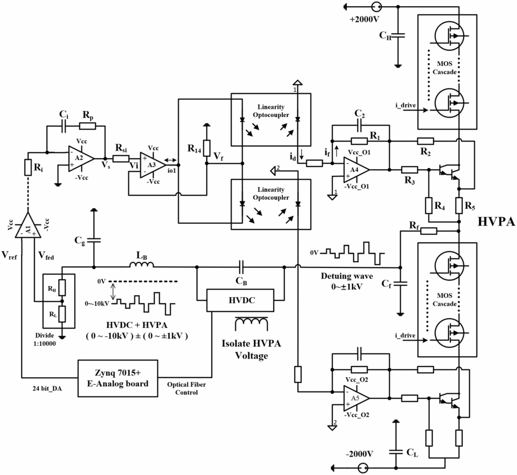
Fig.7 Overall structure of the detuning power supply and its feedback control method
In the current series negative-feedback circuit, the mutual inductance gain of the peripheral circuit composed of operational amplifierA3is set asAgsf, the input voltage asVs, the input voltage of the operational amplifier in the same direction asVi, and the closed-loop gain asAgf;the open-loop gain of the operational amplifier is nearly infinite, whereas the closed-loop input resistance is set asRif, and the optocoupler drive current is set asio1and the feedback coefficient asFr.Therefore, the conditions for achieving deep negative feedback are as follows:
Because theRifis significantly higher thanRsi,
In the voltage-parallel negative feedback circuit, the closed-loop mutual resistance gain of the operational amplifiersA4andA5is set asArf, the optocoupler output to the operational amplifier current asid, the feedback current asif, the feedback impedance asZf, and the feedback coefficient asFg.Therefore, the conditions for achieving deep negative feedback are as follows:
To improve the relative stability of HVPA, deep feedback should be utilized to achieve the state of |1 + AF|≫ 1[18].Thus, the Darlington transistor with a large beta was selected to improve the open-loop gain.Based on the presented analysis, the slew rate of the output voltage of the HVPA in the load of the fixed capacitive ET gun primarily depends onFr,Fg, andKp=Rp/Ri, whereas the rapid stability mainly depends onC2inFgandKi= 1/ (RiCi) in the feedback control.
Assuming that the optocoupler output resistance isRD,since the feedback resistanceR1is generally less thanRD,the zero frequency of the voltage-parallel negative feedback circuit can be concluded to be always lower than the pole frequency.Furthermore, the optimal pole frequency setting based on the system stability was achieved when the relative frequency was located on an open-loop gain curve.The pole frequencyf= 1/(2πR1C2) indicates that the high-frequency asymptotic line of the noise gain is only determined by theC2value.The open-loop gain of this system can be simplified as follows [19]:
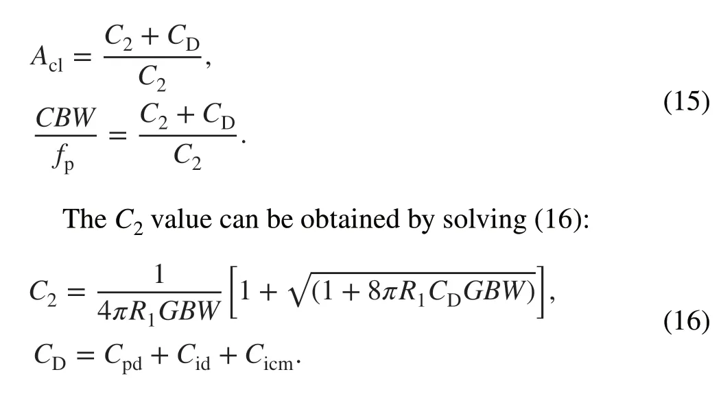
TheCpdis the linear optocoupler output inherent capacitance,Cidis the op-amp differential capacitance,Cicmis the op-amp common-mode capacitance, andGBWis the gain bandwidth product of the operational amplifierA4.
To facilitate further analysis of the influence of various parameters of the series structure of the HVPA and highvoltage DC on the detuning waveform, the overall transfer function model of an equivalent detuning power supply with nonzero initial conditions was established in this study.This was achieved by simplifying the MOSFET, Darlington transistor, and external driving excitation source, as described by the formula below.

Table 3 Summary of specifications and design parameters of the detuning power supply prototype
Theβvalue is the amplification factor of the Darlington transistor, andλis the ratio of the gate current to the drain current of the MOSFET in the symmetrical cascade.The formulae for calculatingA1,A2,B1,B2,C1,C2,D1,D2,E1,andE2are shown in the appendix.
The main decisive factors influencing the ability of the detuning power supply to achieve the pulse within a rise/fall time of 500 μs are the load capacity of the ET-gun and theKp,Fg,Frof the deep negative feedback formula analyzed above.The peak-to-peak voltage of the HVPA output ripple is primarily related to the steady-state performance of the design parameters.Hence, the parameters of the detuning power supply are optimized and simulated under ideal conditions using the transfer function in Eq.(17), which provides a powerful rationale for the prototype design in Sect.IV.The specifications and prototype parameters of the detuning power supply are listed in Table 3.Figure 8a presents the simulation of the optimized overshoot and oscillation of the output waveform of the detuning power supply by adjusting the parametersKp,Fg, andFr.BecauseFgandFrcan be easily determined by designing the component parameters of the required circuit, we first fixed theFgandFrparameters and optimized the waveform by changingKp.If changingKpcauses the system to attain the expected rise time when the flat-top oscillations cannot be eliminated by adjustingKi,it is necessary to further fine-tuneFgandFrand combineKpfor optimization.The optimized rise time is controlled within 500 μs, and the overshoot and oscillation of the rising edge are well-improved.The Bode diagram in Fig.8b shows the passband of the optimized detuning power supply reaching 10 kHz, which satisfies the response-time requirement of the DR detuning waveform.

Fig.8 (Color online) Results of the HVPA output simulation.a Simulated comparison of the detuning power supply with the optimized and unoptimized parameters.b Bode diagram of the detuning power supply after parameter optimization
4 Experimental results
A prototype of the detuning system is developed using the design parameters verified by the simulation described in Sect.3.The main auxiliary power supply in the system can produce soft-switching zero-current sinusoidal waveform outputs at 22 kHz with less than 15% of harmonic components.Figure 9 presents the sinusoidal voltage waveform of the measured LCC series–parallel resonant converter output and the current of the converter in the soft-switching state.The yellow C1 and orange C3 lines represent the gate drive signals of the IGBT.The green C2 line represents the resonant current.The resonant current achieved a softswitching zero-current working state during the dead time of the IGBT gate-drive signal.The blue C4 line represents a high-frequency resonant sine waveform, and its harmonic proportion is less than 15%.
The high-precision setting of the DR waveform and the timing of the detuning power supply were managed by the developed controller.The maximum output voltage test ofthe 5 nF load was conducted by using a 1:10,000 high-precision high-voltage divider.The DC ripple, pulse top ripple,and pulse rise/fall edge times satisfied all the design requirements.The detuning power supply and test results for the complete DR sweeping period are shown in Fig.10.The oscilloscope displays the DR sweep voltage of 0 to ± 1000 V with an offset of −10 kV.The designed high-voltage divider adopts a two-way voltage output, one of which is used as the input of comparatorA1shown in Fig.7, and the other is used for voltage monitoring.
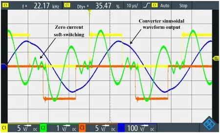
Fig.9 (Color online) The sinusoidal waveform output by the LCC series–parallel resonant converter and the current of the converter in the soft-switching state are measured

Fig.10 (Color online) Detuning power supply and its test results of the complete DR scanning period
The test result of the ± 1 kV pulse voltage floating above the −10 kV DC voltage is shown in Fig.11.The rise/fall time of the pulse are both less than 500 us.The front-stage energy storage capacitors (200 nF) assist in reducing the front-stage ± 2 kV high-voltage power supply output instantaneous current despite them operating with the maximum output detuning voltage at an equivalent ET gun load (5 nF).The rise time of the 1 kV pulse is 180.3 μs, and the fall time is 323.7 μs.The rise/fall times satisfied the design requirements.The difference between the rise/fall times arises from the differentFgparameters between the positive and negative symmetrical cascades.DifferentFgparameters can prevent positive and negative symmetrical cascades from simultaneously turning on during the power-on process.The rise time of the simulation detuning pulse shown in Fig.8a is 230 μs;the trend of the rise time of the pulse shown in Fig.11 is faster than the simulated rise time.This is mainly because the use of the same simulation parameters on the positive and negative symmetrical cascades will lead to the problem of turning on both sides simultaneously; the positive pulse parameters are adjusted based on the simulation.In addition, the rise time of the detuning pulse is affected by thedrive of the multiple MOSs, and active components such as multiple MOSs are idealized and replaced in the simulation.As shown in Fig.12a, the ripple in the HVDC output at 1000 V exceeds 100 ppm.However, within the normal DR experimental range, HVDC output ripples of greater than 2000 V can be limited to the 100 ppm range.The HVDC cannot meet the specifications at low voltages owing to the background noise.Figure 12b and c also demonstrate the ripple waveform and ripple FFT, respectively, at the maximum output.The main ripple harmonic components were 22 kHz and were high-order harmonics.This is because the system adopts a floating and in-series structure, which disturbs the power-supply ripple owing to the isolated power supply.The ripple of the detuning power supply is subject to the conducted and radiated interference from the isolated power supply.A greater output power of the isolated power supply results in stronger interference.In addition, an effective solution is to maintain the high-frequency source distant from the experimental equipment, use the relevant electromagnetic shielding, and suppress the related common-mode interference.

Fig.11 (Color online) Maximum output voltage test.The bright blue line is the overall output of the detuning power supply.(−10 k VAC ± 1000 V DC).The pulse rise time measured by the oscilloscope is 180.3 μs.The green line is the output current of the front-stage positive power supply in HVPA.The pink line is the output current of the front-stage negative power supply in HVPA
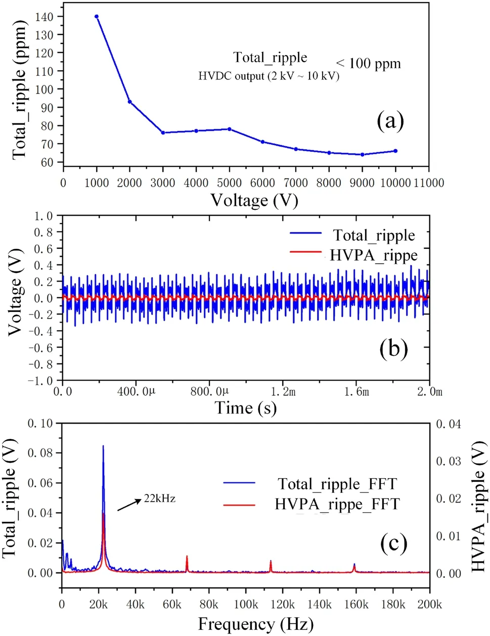
Fig.12 (Color online) The ripple test for the output maximum detuning voltage.The test uses a C-R circuit (C = 20 nF, R = 100 MΩ) to indirectly measure the ripple of the detuning voltage under the condition of long pulse widths.a The blue line is the overall ripple voltage of the HVDC output ranging from 1 to 10 kV, measured with the HVPA output maximum of 1000 V.b The red line is the ripple of the HVPA output at 1 kV.The blue line is the ripple at the top of the overall output detuning voltage (−10 kV + 1000 V).c The waveform is the FFT of the middle two ripples
To understand the performance of the developed electron-energy fast detuning system, we first installed the prototype on a CSRm electron cooler [20] and tested it with an online DR experiment for Li-like Fe15+ions.In the experiment, the Li-like Fe15+ions were produced from an ECR ion source and accelerated to a beam energy of 4.35 MeV/u by a sector-focused cyclotron and then injected into the cooler storage ring CSRm [21].The electron cooling HV was set at −2368.5 V, and the electron current was 46 mA, under which the electron and ion beam are velocity-matched, that is, the electron and ion beams have the same mean velocity in the longitudinal direction and the relative energy between these two beams is zero.The main parameters of all the power supplies for the electron gun are listed in Table 1.
After the electron cooling was done for several seconds, the momentum spread ( Δp∕p) of the injected ion beam was reduced to approximately 1.75×10⁻⁴.In the DR measurement, the electron energy was scanned from 0 to ± 360 V in the entire measurement cycle.For each detuning voltage point, the electron energy was detuned for 20 ms and set to the cooling point (Erel=0 ) for 180 ms to maintain a good ion beam quality.The relative energy between the electron and ion beams at the cm frame was calculated using the following formula:
wheremeandmiare the electron- and ion-resting masses,respectively;cis the speed of light,γeandγidenote the Lorentz factors of the electron and ion beams, respectively.υe=βecandυion=βicare the velocities of the electron and ion beams.The angleθbetween the electron and ion beam was safely assumed to be zero in the current experiment.The space-charge effects were carefully considered, and the drag-force effects were found to be negligible.For electron–ion recombination experiments at heavy ion storage rings, the recombination rate coefficientαcan be deduced from the recombination counting rateRat a relative energyErelbetween the electron and ion by the following [22]:
whereNiis the number of stored ions,neis the density of the electron beam,Lis the length of the effective interaction section, andCis the circumference of the storage ring.
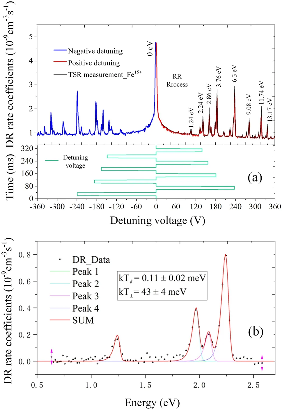
Fig.13 (Color online) Result of the DR demonstration experiment.a Comparison of the measured DR spectrum with the TSR; the abscissa is expressed by the voltage value.b Fitting of the longitudinal temperature to the broadening of the DR resonance peak between 1 and 2.5 eV
According to Eqs.(18) and (19), the obtained electron–ion recombination spectra are shown in Fig.13.The recombination spectra measured under the positive and negative detuning voltages are represented by the solid red and blue curves, respectively.The spectra cover an electron–ion collision energy of 0–15 eV, encompassing part of the DR resonances owing to the 3s→ 3pand 3dcore excitations.The strong peak at 0 eV clearly indicates the contribution of the radiative recombination (RR) process.The resonant positions in Fig.13a and the corresponding detuning voltages are shown in the lower panel.We also compared the measured DR spectra with the experimental results from the TSR measurement in detail [23]; the resulting resonant parameters were in good agreement.The ripple of the power supply affected the longitudinal temperature of the electron beam, and the change in the longitudinal temperature was reflected in the broadening of the DR resonance peak.By fitting the longitudinal temperature to the broadening of the DR resonance peak shown in Fig.13b between 1.0 and 2.5 eV and using the constant parameter (C= 2) to calculate Eq.(23) [24, 25,26], the results demonstrate that the ripple of the power supply was approximately 116 ppm.The main reason for the difference between the theoretical calculation and power supply test results is that the theoretical longitudinal temperature is affected by many factors, such as the space charge effect, longitudinal-longitudinal relaxation,and cathode temperature.Although the calculated results are not consistent with the measured results, it is highly likely that the broadening of the DR resonance peak is compatible with the ripple measurement.
5 Conclusion
In this study, the analysis and design of the main auxiliary power supply with an LCC series–parallel resonant converter in the front stage and an LC filter structure in the poststage are introduced, which can provide power transmission with low harmonics and low switching noise and protect the system in extreme cases.Based on the DR experimental waveform requirements and ET-gun load characteristics, a high-voltage detuning power supply with HVPA and HVDC modules in series was designed.The implementation and practical considerations of the overall structure of the detuning power supply were described.The proposed method achieves a large instantaneous current of the HVPA output and solves the simultaneous conduction of the positive and negative symmetric cascades of the HVPA.
The designed auxiliary power supply was used to provide a high-frequency isolated power transmission for detuning the power supply.The 0 to ± 1 kV detuning pulses floating above 0 to −10 kV DC were achieved on an equivalent ET gun load (5 nF) using the designed special detuning power supply.The pulse ripple was less than 100 ppm, and the rising or falling edge was less than 500 us, which met the requirements of the DR experiment.According to the DR experimental parameters of the experimental ion Fe15+, the 0 to ± 360 V pulses floating above the high voltage −2368.5 V DC output of the system were used for the DR test.The resonant parameters of the experimental results were consistent with those of the DR test of the TSR, which verified that the detuning system achieved the proposed technical indicators.
The presented results demonstrate the reliability and feasibility of this newly designed electron energy detuning system, which also provides an early technical reserve and paves the way for the future contraction of the detuning system for the SRing electron target.In addition, the designed detuning power supply provides an applicable technical solution for driving capacitive loads, such as electron guns, to achieve fast rising or falling edges and low top-ripple linear high-voltage pulses.
Appendix
The componentsa,c, andeused in the imaginary transfer function calculation described in Eq.(1) were obtained using the following formula:
The componentsφ1,φ2,andφ3used in formula (11) can be obtained by the following:
The componentsA1,A2,B1,B2,C1,C2,D1,D2,E1, andE2in the transfer function of the equivalent detuning power supply described in Eq.(17) are obtained by the following formula:
Author contributionsAll authors contributed to the study conception and design.Material preparation, data collection and analysis were performed by Kai-Ming Yan, Ming-Rui Li, Yun-Bin Zhou, Xiao-Ming Ma, Jin-Bin Shangguan, Zhong-Kui Huang, Xiao-Jun Wang,Mei-Tang Tang, Jie Gao, Hou-Ke Huang, Da-Qin Gao and Li-Jun Mao.The first draft of the manuscript was written by Kai-Ming Yan and all authors commented on previous versions of the manuscript.All authors read and approved the final manuscript.
Data availabilityThe data that support the findings of this study are openly available in Science Data Bank at https:// www.doi.org/ 10.57760/ scien cedb.07941 and https:// cstr.cn/ 31253.11.scien cedb.07941.
Declarations
Conflict of interestThe authors declare that they have no competing interests.
杂志排行
Nuclear Science and Techniques的其它文章
- GPU‑based cross‑platform Monte Carlo proton dose calculation engine in the framework of Taichi
- Simple synthesis of silver nanocluster composites AgNCs@PE‑g‑PAA by irradiation method and fluorescence detection of Cr3+
- Photonuclear production of nuclear isomers using bremsstrahlung induced by laser‑wakefield electrons
- Resolution analysis of thermal neutron radiography based on accelerator‑driven compact neutron source
- Decomposition of fissile isotope antineutrino spectra using convolutional neural network
- Searching for QCD critical point with light nuclei
