Evolution of microstructure,stress and dislocation of AlN thick film on nanopatterned sapphire substrates by hydride vapor phase epitaxy
2023-03-13ChuangWang王闯XiaoDongGao高晓冬DiDiLi李迪迪JingJingChen陈晶晶JiaFanChen陈家凡XiaoMingDong董晓鸣XiaodanWang王晓丹JunHuang黄俊XiongHuiZeng曾雄辉andKeXu徐科
Chuang Wang(王闯) Xiao-Dong Gao(高晓冬) Di-Di Li(李迪迪) Jing-Jing Chen(陈晶晶)Jia-Fan Chen(陈家凡) Xiao-Ming Dong(董晓鸣) Xiaodan Wang(王晓丹)Jun Huang(黄俊) Xiong-Hui Zeng(曾雄辉) and Ke Xu(徐科)
1School of Nano-Tech and Nano-Bionics,University of Science and Technology of China,Hefei 230026,China
2Suzhou Institute of Nano-tech and Nano-bionics,Chinese Academy of Sciences,Suzhou 215123,China
3Jiangsu Key Laboratory of Micro and Nano Heat Fluid Flow Technology and Energy Application,School of Physical Science and Technology,Suzhou University of Science and Technology,Suzhou 215009,China
4Shenyang National Laboratory for Materials Science,Jiangsu Institute of Advanced Semiconductors,Suzhou 215000,China
5Suzhou Nanowin Science and Technology Co.,Ltd.,Suzhou 215123,China
Keywords: hydride vapor phase epitaxy (HVPE), AlN, threading dislocations, nano-patterned sapphire substrate
1.Introduction
AlGaN-based deep-ultraviolet (DUV) optoelectronic devices have attracted much attention in the field of air and water purification,sterilization,and medical applications.[1-4]At present, AlGaN based DUV devices are fabricated on AlN templates due to the lack of native substrates.[5]Hydride vapor phase epitaxy(HVPE)is currently one of the most promising methods to produce industrial grade AlN templates due to the high growth rate and low impurity concentration.[6-8]However,the large lattice and thermal mismatch between sapphire and AlN always result in very high threading dislocation density (TDD) as well as large strain in AlN films.The performance of the AlGaN-based devices is seriously limited by the quality of the template.[9-11]A high-quality AlN thick film will be beneficial to reducing the stress and dislocation density of the following AlGaN epitaxial layer.Therefore, it is crucial to grow high-quality AlN thick films for improving the performance of the AlGaN-based devices.
Many growth techniques/methods have been developed to improve the quality of AlN thick films on sapphire substrates,such as multilayers via growth mode alternation technique,[12]migration-enhanced metal-organic chemical vapor deposition(MEMOCVD),[13]sapphire nitridation pretreatment,[14]lateral overgrowth on patterned sapphire substrates,[15]hightemperature annealing[16]andin situetching method.[17]Among these methods, the lateral overgrowth method on NPSSs has attracted much attention for its effectivity in reducing dislocation density and stress.[18,19]It is reported that the AlN epilayer grown on hole-type NPSS by metal-organic chemical vapor deposition (MOCVD) can achieve higher quality attributed to the center-closed growth mode.[20]Although the growth of parasitic grains on the additional surface introduced by NPSS can affect coalescence and possibly seriously affect the crystallinity of the epitaxial layer,[21-23]the voids caused by the lateral growth process of the AlN columns on the mesa provide a channel for the gradual release of the stress.[24]However, there are few reports about HVPE-AlN layers grown on hole-type NPSSs and the stress and dislocation evolution process remain unclear.
In this report,AlN thick films were grown on hexagonally arranged concave truncated cones shaped hole-type NPSSs in a home-built horizontal HVPE system.The surface morphology, crystal quality, and the evolution behavior of stress and threading dislocations are investigated in detail,which would be beneficial for the growth of high-quality AlN films.
2.Experiments
Commercially available 2-inch c-plane-oriented NPSSs were used in this work.Figure 1(a) shows a typical AFM image of NPSSs with hexagonally-arranged hole-type pattern.The pattern period is~1 µm.The cross-sectional profile is shown in Fig.1(b).The inside structure of the hole is an inverted truncated cone.The depth and diameter of holes are approximately 500 nm and 815 nm, respectively.The AlN thick films with about 4.5µm thickness were grown on NPSSs in a home-built HVPE setup.In the experiments, the substrates were heated at 1500°C in a mixed carrier gas flow(N2:H2=1:1).As a reactive gas, AlCl3was generated in the reactor (source zone) by the reaction between Al metal and HCl gas at 550°C, and was then reacted with NH3in the growth zone.The HCl and NH3flow rates are 60 sccm and 800 sccm,respectively.And the carrier gas flow rate of mixed N2and H2is fixed at 2000 sccm.
The surface morphology and structure of the AlN films were characterized by atomic force microscopy(AFM)in tapping mode.The cross-sectional morphologies of samples were examined by scanning electron microscopy (SEM) by using Hitachi S4800.The crystallinity and stress of the AlN films were determined by high-resolution x-ray diffraction(HRXRD) and Raman scattering (Raman line scan was performed every 0.1µm for a test point),respectively.Transmission electron microscopy(TEM)and scanning TEM(STEM)measurements were performed through a TALOS F200X operating at 200 kV.The cross-sectional specimens were prepared along the[11¯20]AlN direction by mechanical polishing, and then by Ar+ions milling.
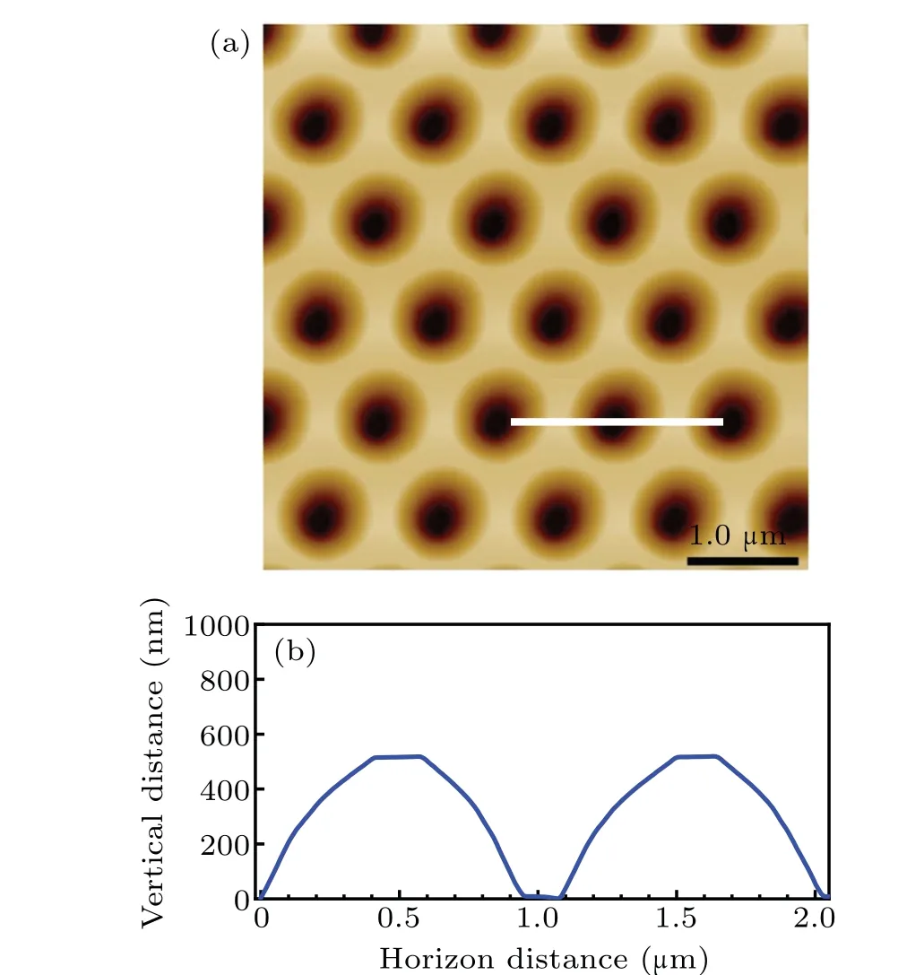
Fig.1.(a)AFM image of hole type NPSSs.(b)Cross-section profile of the patterns at the white solid line in(a).
3.Results and discussion
Figure 2 exhibits that the full width at half-maximum(FWHM) values of symmetric (0002)- and asymmetric(10¯12)-planes x-ray rocking curves (XRCs) of the AlN thick films are 405 arcsec and 647 arcsec, respectively.An estimation of the dislocation densityρshould be calculated by the equationρ=β2/4.35b2,[25]whereβtilt andβtwist are the FWHMs of the(0002)and(10¯12)XRC,respectively,and the Burgers vectorbis equal toc-axial anda-axial lattice constants, respectively.The screw- and edge-type dislocation densities were calculated to be about 6.62×108cm-2and 3.08×109cm-2,respectively.
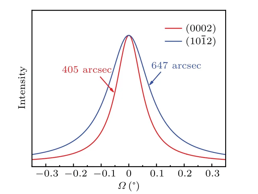
Fig.2.XRCs for(0002)and(10¯12)planes.
Figures 3(a) and 3(b) show the surface morphology of AlN layers grown on NPSSs.As shown in Fig.3(a), the surface of the AlN layer has complete coalesced and shows multiple growth spirals.This may be due to the periodically distributed TD source below the coalesced surface.[26]The root mean square (RMS) value of surface roughness for a 10×10 µm2area is 1.35 nm.In addition, the smooth and uniform step-flow morphology is observed in Fig.3(b).The RMS value for a 2×2µm2area is 0.24 nm.Figure 3(c)shows the cross-sectional morphology of epilayer.It is found that the epilayer prefers to merge on the patterned regions and voids are formed over the hole of NPSSs.The average coalescence thickness is about 2µm,which is similar to previous reports.In addition, the void deviates from the center of the pattern,which may correspond to the coalescence process of the surface.On the other hand,misaligned crystallites were observed on the sidewall of sapphire,which is confirmed by TEM measurement later.It is reported that the HVPE-AlN layers nucleate and grow simultaneously both on the mesa and sidewall of NPSSs.[27]The parasitic AlN crystallites which orientation is different from the orientation of the AlN layer on the c-plane mesa decelerated the coalescence process of layers, and resulted in the void deviates from the center of the pattern.
In order to study the surface coalescence behaviors, the sample was obliquely dissociated.Figure 4(a) shows the oblique cross-sectional morphology image of the AlN layer,which can demonstrate the evolution of void outlines at different thickness.It is found that a large number of the triangular hollow profiles are periodically distributed on the plane.The cycle of the voids is consistent with the period of the NPSSs pattern exactly.The extended outlines are at an angle of 120 degrees to each other, and one of them is parallel to [11¯20]direction.And the area of voids decreased gradually with increasing of epilayer thickness during the growth process.Figure 4(b) presents a magnified image at the AlN/NPSSs interface.The three-fold distributed inclined grains grown on the slopes of the NPSSs were observed on the interface,and have the same spatial distribution as the void.It is speculated that the undesired AlN crystal grown on the sidewalls of the holes may hinder the growth of c-oriented AlN on the mesa area,and thus, the coalescence of the holes presents a triangular void morphology.
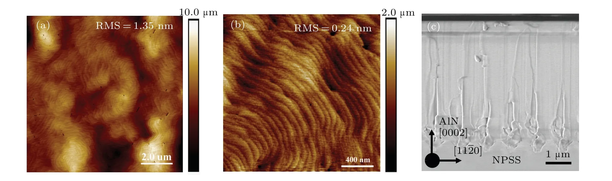
Fig.3.(a)AFM image of the surface morphology.(b)Magnified morphology in(a).(c)Cross-sectional SEM image.
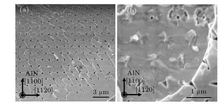
Fig.4.(a)Oblique cross-sectional SEM images of AlN layers.(b)SEM images of three-fold distributed misaligned crystal on AlN/Sapphire interface.
Figure 5(a) shows the cross-sectional bright-field STEM image underg= [0002] condition.It can be seen that the profile of nanohole is different from the original morphology due to the decomposition of sapphire at high temperature.[28]The crystal orientation on three positions (marked by yellow circles) is confirmed by the selected area electron diffraction(SAED).Positions 1 and 2 are located at the region of crystal grown on the left and right sidewall of the hole, respectively,and position 3 is at the mesa region.The SAED results reveal that the orientation of grains grown on these positions is completely different.As shown in Figs.5(b)and 5(c),[11¯20]and [0002] orientation AlN were grown on the right and left sidewall, respectively.This phenomenon is similar to other group III nitrides growing on different orientation sapphire substrate.[29,30]As shown in Fig.5(d),a c-plane AlN layer was grown with a 30°rotation around the[0001]axis with respect to the sapphire,and the epitaxial relationships are AlN(0002)||sapphire(0006)and AlN(10¯10)||sapphire(11¯20).[31]
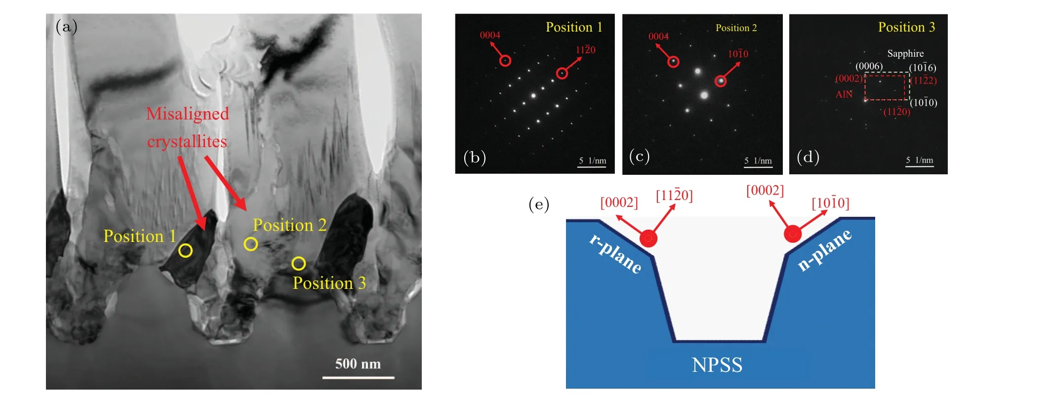
Fig.5.(a) Cross-sectional bright-field STEM image under g=[0002] condition.(b)-(d) The SAEDs of three positions as marked in (a).(e)Illustration of crystal orientation parasitic grains.
The angle between the inclined non-c-plane sidewall of NPSSs and the c-plane is close to that between r- or n-plane sapphire and c-plane sapphire, indicating that the r- and nplane sapphire facets may be contained in the NPSSs.The AlN nucleation on NPSSs takes place not only on the c-plane mesa areas but also on the inclined sidewalls of the hole containing r-and n-facets(misaligned crystallites).[22]In the initial stage of growth, the parasitic crystallites formed on the sidewall of nano-hole are competing with AlN crystals grown on the mesa and are eliminated during the subsequent lateral growth of the epitaxial layer.Figure 5(e)shows a schematic of the crystal orientation of parasitic AlN crystals grown on the upper inclined plane of NPSSs.Based on the SAED measurements, the AlN crystallites which hinder surface coalescence are assigned to the misaligned grains formed on the three-fold n-plane of sapphire substrates.[32]So,it can be concluded that the appearance of unique triangular voids is caused by the presence of parasitic crystallites existed in this specific area.
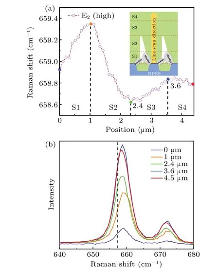
Fig.6.(a) Evolution of the E2 (high) phonon mode frequency shift along growth direction.The inset image is a schematic diagram of the Raman line scan measurement.(b) Raman spectra of epilayer at five typical positions.The dashed line corresponds the E2 (high) peak of bulk AlN at 657.4 cm-1.
The stress evolution of HVPE-AlN films grown on the mesa of NPSSs was characterized through Raman spectroscopy.Figure 6 shows the evolution of E2(high) phonon mode frequency with the growth direction and the Raman spectra of epilayer on five typical positions,which reveals the stress evolution of samples with thickness.It is found that the phonon frequency of E2(high)fluctuates greatly along the growth direction.And the fluctuation can be roughly divided into four stages S1-S4 were given in Fig.6(a).The inset image is a schematic diagram of the Raman line scan measurement.Since the peak of the E2(high)phonon mode of stressfree AlN locates at 657.4 cm-1,there is residual compressive stress in the AlN layer.[33]Just above the heterointerface, the compressive stress of AlN increases continuously and reaches its peak position (1 µm), which is resulted from the combination of thermal expansion coefficient (TEC) mismatch between AlN and sapphire and the competitive growth process in the early stages of growth.It is found that the E2(high)phonon frequency decreases gradually from 659.4 cm-1to 658.6 cm-1in the S2 stage,which corresponds to the coalescence evolution process of the AlN layer as discussed above.The presence of nanovoids act as a stress releasing channel in the growth direction.[24]The E2(high) phonon mode frequency in the S3 stage with a certain rebound may be caused by the misorientations of the adjacent regions at the coalescence region.And it enters a stable state after fully completing the coalescence.
In order to examine the dislocation annihilation mechanism of AlN layers, the cross-sectional dark-field TEM images were taken as shown in Fig.7.Figures 7(a)and7(b)show the same area of the AlN epilayer on NPSSs under two-beam condition withg=[0002]and[11¯20],respectively.According to the invisibility criterion rule,g·b=0, the edge, mix, and screw dislocations were identified by comparing the two TEM images of the same area under different diffraction conditions.The screw-type and edge-type TDs are visible withg=[0002]and [11¯20], respectively.[34]The mix-type TDs generated on the coalescence position is countable and is caused by the misorientation of the adjacent regions.In contrast, the number of edge-type dislocations is relatively higher and many of them can propagate into the upper AlN epilayer, as shown in Fig.7(b).It is noted that there is a significant strain contrast above the mesa,which is associated with large compress stress caused by the competitive growth between the parasitic crystallites and AlN grown on the mesa area.
To illustrating the evolution process of the TDs more clearly, the magnified images of the heterointerface enclosed in the red rectangle were presented in Figs.7(c) and 7(d).It is clear that there is a lot of inversion domains(IDs)as shown in Fig.7(c).The Burgers vector of these IDs is similar to the Burns vector of the spiral dislocations, making it difficult to determine the origin of the spiral dislocations generated on the mesa.[35]As shown in Fig.7(d),the edge TDs(type-D)generated at the AlN/sapphire interface interacted with each other,resulting in a decrease in the threading dislocations density(TDD)above the mesa regions.A part of dislocations with different signs spontaneously form dislocation loops.Due to the image force effects,the rest of the TDs near the nanohole bend toward and terminate the boundary.In addition,the connection of TDs with the same signs generated at the crystal boundary(type-C) results in the appearance of horizontal dislocation.These mechanisms all lead to the effectively reduction of dislocations.However,the TDD increases apparently during the subsequent epitaxy process.It is because the probability of dislocation reaction is inversely proportional to the spacing between them.A large number of edge-type TDs generated on the boundary of misaligned crystallites (type-B) hardly interact with each other,extend directly to the upper AlN epilayer.
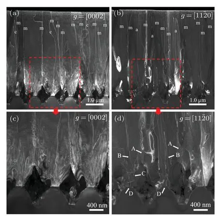
Fig.7.Cross-sectional dark-field TEM images under two-beam conditions(a)g=[0002],(b)g=[11¯20].(c)and(d)The magnified images of selected typical zones in(a)and(b),respectively.
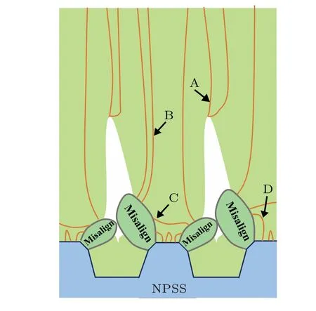
Fig.8.Illustrations of TDs distribution in AlN epilayers grown on NPSSs.
Figure 8 is the schematic diagram of the distribution of dislocation.There are two type of TD that propagated into the surface of epilayers.The mixed-types TDs(type-A)is caused by the misorientation of the adjacent regions during the coalescence of voids.And the pure edge-type TDs(type-B)are originated from the boundary between the misaligned grains and the AlN on mesa.It is reported that the effects of image force and misorientation should be taken into account for decreasing the TDD in AlN epilayers grown on NPSSs.[36]However,for the NPSSs with inverted truncated cone-shaped pattern,the misaligned crystallites should also be considered.The type-B TDs formed at the boundary becomes a crucial factor leading to the deterioration of the crystalline quality of AlN films.It is supposed that the crystal quality of AlN thick films will be improved by decreasing the dimension of misaligned grains.
4.Conclusion and perspectives
In summary,the formation mechanism of triangular voids in the HVPE-AlN epilayer grown on concave truncated coneshaped NPSSs and its effect on crystal quality are investigated.It is found that c-orientation AlN grown on the mesa are hindered by the undesired parasitic nucleation on the three-fold n-plane facet sapphire,which results in the presentence of the holes with a triangular outlines morphology.The Raman measurements indicate that the appearance of voids can effectively relieve compressive stress produced by the undesired grain growth and the coalescence of misaligned AlN.In addition,reduction of parasitic growth on the sidewall of pattern is also essential for decreasing TDD in the upper AlN epilayer.
Acknowledgements
Project supported by the National Natural Science Foundation of China(Grant No.61974158)and the Natural Science Fund of Jiangsu Province,China(Grant No.BK20191456).
猜你喜欢
杂志排行

Chinese Physics B的其它文章
- Matrix integrable fifth-order mKdV equations and their soliton solutions
- Comparison of differential evolution,particle swarm optimization,quantum-behaved particle swarm optimization,and quantum evolutionary algorithm for preparation of quantum states
- Explicit K-symplectic methods for nonseparable non-canonical Hamiltonian systems
- Molecular dynamics study of interactions between edge dislocation and irradiation-induced defects in Fe-10Ni-20Cr alloy
- Engineering topological state transfer in four-period Su-Schrieffer-Heeger chain
- Spontaneous emission of a moving atom in a waveguide of rectangular cross section