Review of a direct epitaxial approach to achieving micro-LEDs
2023-02-20YuefeiCai蔡月飞JieBai白洁andTaoWang王涛
Yuefei Cai(蔡月飞), Jie Bai(白洁), and Tao Wang(王涛),‡
1Department of Electronic and Electrical Engineering,Southern University of Science and Technology,Shenzhen 518055,China
Keywords: micro-LED,epitaxial growth,gallium nitride,display
1. Introduction
With the advent of “5G era” which is expected to penetrate into every aspect of our daily life, a number of new optoelectronics will have to be developed to meet a wide range of applications, such as augmented reality and virtual reality (AR and VR) devices, microdisplays for smartphones and smart-watches, autodisplay, next generation TV, where III-nitride based micro light-emitting diodes(μLEDs)are the key components.[1–4]AR&VR micro-displays which require μLEDs with ultra-small dimensions are typically utilized in small spaces or at close proximity to the eye. Therefore,such a microdisplay needs to exhibit high resolution,high contrast ratio,high luminance,high external quantum efficiency(EQE)and narrow spectral linewidth. Yole D´eveloppement has predicted that the global microdisplay market will reach$4.2 billion by 2025 at a compound annual growth rate (CAGR) of 100%.
The III-nitride μLEDs demonstrate many unique advantages over either organic LEDs (OLEDs) or liquid crystal displays (LCDs). For example, III-nitride based microdisplays,where μLEDs are the essential components and are selfemissive, exhibit much higher resolution, higher efficiency,and higher contrast ratio than either OLEDs or LCDs. Furthermore, III-nitride μLEDs display much longer operation lifetime and much stronger chemical robustness than either OLEDs or LCDs.[1–4]Generally speaking, μLEDs with a dimension of≤100 μm are typically used for the fabrication of autodisplay and next-generation TV,while AR/VR devices require μLEDs with a dimension of≤5 μm. In addition,ultra-small μLEDs exhibit significantly reduced junction capacitance due to their physical dimension, which is crucial for achieving a high-speed data transmission rate with a GHz modulation bandwidth that is necessary for visible light communication(VLC)applications.[5,6]
So far, III-nitride μLEDs are basically fabricated by using standard photolithography techniques and dry-etching processes.[7–12]It is well-known that dry-etching processes unavoidably bring substantial damages to the surface and the sidewalls of LEDs, which enhance non-radiative recombination leading to reduction in optical performance.[13–18]This may be a minor issue and can be negligible in the case of the fabrication of standard LEDs with a dimension of≥100 μm.However, this issue cannot be ignored anymore when the dimension of μLEDs decreases down to the tens micrometer scale and eventually becomes a major factor which is responsible for severe degradation in optical performance.[14,15,19]To be more specific,it is necessary to comment three major challenges which conventional dry-etching methods are facing before a proposed idea can be put forward.
Drying etching processes such as inductively coupled plasma (ICP) dry etching techniques have been widely used to define either broad area LED mesas or μLED mesas in the semiconductor industry. As stated above, dry-etching technologies unavoidably lead to a significant reduction in the quantum efficiency of μLED compared with large area LEDs.Although the passivation technology has been used aiming to reduce plasma induced damages on the sidewalls of μLEDs during dry-etching processes, the improvement is marginal even if an advanced atomic layer deposition (ALD) technique is used instead of a standard plasma-enhanced chemical vapor deposition(PECVD)technique.[14]This passivation procedure also generates an extra issue, namely, the etching back of the dielectric layer on top of the p-contact/p-GaN of μLEDs,potentially degrading electrical injection in the p-GaN region.[13]This becomes particularly challenging for the fabrication of ultra-small μLEDs, such as μLEDs with a dimension of≤5 μm. Consequently, the EQE of the μLEDs with a dimension of≤5 μm is very low and is limited to 1% to 5%, meaning that such μLEDs cannot meet the requirement for AR/VR applications. Very recently, it has been reported that severe damage on the sidewalls of the μLEDs has been clearly observed on blue μLEDs with a dimension of≤5 μm in a square shape.[20]This also means that it is extremely challenging to apply the conventional fabrication approaches which mainly combine a standard photolithography technique and subsequent dry-etching processes in obtaining ultra-small μLEDs with satisfied performance.
Conventional III-nitride LEDs exhibit a broad spectral linewidth due to the nature of InGaN alloys which are used as an emitting region. A significant reduction in the spectral linewidth of μLEDs is necessary for achieving microdisplays with high resolution especially for AR and VR.Generally,In-GaN LEDs exhibit an intrinsically broad spectral linewidth mainly due to indium segregation and alloy fluctuation. This becomes more severe with increasing emission wavelength,as higher indium content InGaN is required to obtain a longer emission wavelength. It is necessary to develop a new approach or process to overcome the fundamental limitations,allowing us to not only further increase the EQE of μLEDs but also significantly reduce their spectral line width.
Currently, it is naturally difficult to achieve III-nitride μLEDs with a long-wavelength emission, such as red emission which is one of the three fundamental components for the formation of RGB (red, green, blue) based full color display. So far, InGaN-based μLEDs with reasonably good performance in the blue and green spectral region have been reported. However, it is very challenging to achieve higher indium content InGaN to extend the emission wavelengths beyond the green spectral region while maintaining high optical performance.[21,22]A typical method to achieve higher indium content in InGaN is to lower the growth temperature for In-GaN, but this method is not ideal because it is expected that a reduction in growth temperature generally causes a significant degradation in crystal quality. In general, vapor–solid thermodynamic equilibrium can be modified by stress,making the solid-phase epitaxial composition reduce toward latticematched conditions. This is the major reason why it is so difficult to enhance indium incorporation into GaN.[23–32]Therefore, the growth of InGaN on a relaxed layer is beneficial for obtaining high indium content in InGaN.However,it is worth highlighting that the formation of a relaxed layer is often associated with the generation of extra defects if a heterostructure with a large lattice mismatch is used to generate the relaxed layer.This leads to degradation in optical performance.Inserting a thin AlN or an AlGaN layer into each InGaN quantum well as an emitting region leads to an enhancement in strain that pushes the emission wavelength of InGaN quantum wells toward longer wavelength.[30,31]So far,this approach has become a popular method for the growth of red LEDs,[27–32]but leading to a reduction in the internal quantum efficiency.
Therefore,it is necessary to develop a game-changing approach to the growth and then the fabrication of μLEDs to address all the challenges discussed above. In addition,any new approaches will have to be simplified and scalable to meet industrial requirements in terms of mass-production.
2. Nature and mechanism of the confined selective epitaxy approach
To address the challenges mentioned above,the Sheffield team has proposed and then developed a direct epitaxy approach which we call the “confined selective epitaxy” (CSE)approach[33,34]This direct epitaxy approach is different from either homoepitaxy or heteroepitaxy approach. This is also different from any conventional selective epitaxy approaches.For any conventional selective epitaxy approaches, epitaxial growth is initially carried out within an area which is formed by thin dielectric masks until the growth is above the masks and then epitaxial growth carries on in an unconfined manner along both the vertical direction and the lateral direction. In contrast, for our proposed CSE approach, epitaxial growth is always conducted within a confined area throughout the whole epitaxial growth process. Therefore, the growth mechanism of our CSE approach is entirely different from any conventional selective epitaxy approaches because the masks always confine the epitaxy growth and thus significantly affect the deposition of the epitaxial layers. Furthermore, if the confined area for CSE is smaller, the non-uniformity of atomic deposition becomes more severe. Therefore, it is crucial to develop a new growth procedure to effectively suppress atomic deposition in a non-unform manner during the whole epitaxial growth processes, which is the key to achieve CSE successfully. Of course, the CSE approach allows either photonics or electronics to be naturally formed on a micrometer scale as long as the predefined masks used are on the micrometer scale,meaning that dry etching is not required for the fabrication of μLED mesas(the 1ststep for the fabrication of any semiconductor device)anymore. It means the physical dimension of a device is essentially determined by the dimensions of the predefined masks used for CSE. Therefore, there is no plasma induced damage which always exists during conventional dryetching processes. In principle, unlike either homoepitaxy or heteroepitaxy approach,the CSE approach does not necessarily reply on a substrate used. Another advantage of our CSE is that it is easy to achieve an on-chip monolithic integration of optoelectronics and electronics, where of course no dryetching is needed anymore. Based on our CSE approach, the Sheffield team has achieved ultra-small μLEDs without involving dry-etching processes, leading to the demonstration of ultra-small and ultra-compact μLEDs with a record EQE and small reverse leakage current in the green and red spectral regions.[33,34,36,37]Based on this CSE approach, by epitaxially integrating a microcavity and ultra-small μLEDs, ultrasmall and ultra-compact μLEDs with a stabilized emission wavelength have been achieved,[35]which is extremely important for practical applications and has addressed the longstanding issue in the field of III-nitride optoelectronics. In addition,the CSE approach has also been employed to monolithically integrate μLEDs with high electron mobility transistors(HEMTs)for visible light communication(VLC)and display applications.[38,39]
3. The CSE approach
3.1. Demonstration of ultra-small μLEDs
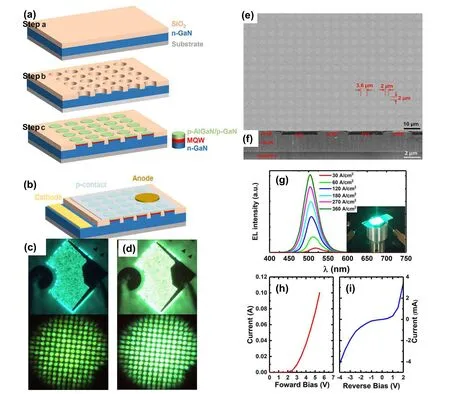
Fig.1. (a)Procedures of our direct epitaxial approach;(b)LED device fabricated on overgrown μLED arrays;(c)μLED emission images at 3 A/cm2;(d)μLED emission images at 9 A/cm2;(e)top and(f)cross-sectional view SEM images of our overgrown μLEDs(diameter: 3.6 μm,spacing: 2 μm);(g) EL spectra, (h) I–V and (i) reverse leakage current of overgrown μLEDs. Reprinted with permission from Ref. [33]. Copyright 2020 American Chemical Society(https://creativecommons.org/licenses/by/4.0/).
For our CSE approach, the first step is to form a selective growth mask on a template, where subsequent epitaxial growth can be carried out in a confined manner throughout the whole growth process. In order to ensure entirely confined selective epitaxial growth,a mask will have to be properly designed and then fabricated in terms of the parameters required for CSE such as sidewalls and thickness.In principle,the used template for CSE can be any structure, either a single GaN on sapphire or silicon or any other substrate, or an epitaxial distributed Bragg reflector (DBR) structure on sapphire or silicon or any other substrate,or a high electron mobility transistor structure on sapphire or silicon or any other substrate,or any other epitaxial layer. For a demonstration purpose, a standard single n-GaN on sapphire is used as a template, on which a SiO2dielectric layer is deposited to form an overgrown mask. By using an inductively coupling plasma technique, the SiO2layer is dry etched to form regularly arrayed micro-holes (where the diameter and the spacing are 3.6 μm and 2 μm,respectively,both of which are able to be tuned according to specific applications), a standard LED structure is then selectively overgrown within the regularly arrayed microholes. The height of the final LED structure has to level with the mask thickness,ensuring that the selective epitaxial growth is entirely confined within the regularly arrayed micro-holes.Finally, regularly arrayed μLEDs are naturally formed without involving any dry-etching processes.[33,34]A detailed procedure is provided in Ref.[33]and cited here in Fig.1(a). The surface of the μLED wafer is flat as shown in Figs. 1(e) and 1(f). The micro-hole arrayed SiO2masks also serve as an insulation layer between individual μLEDs. A layer of indiumtin-oxide(ITO)covers all the p-GaN of μLED arrays and the anode metal is further deposited on it, forming a commonanode structure. For the fabrication of n-contact,the n-GaN is exposed by dry etching down to the n-GaN layer where Ti/Al alloys are deposited. The schematics of the μLEDs arrays,the light emission,the electro-luminescence(EL)spectra,theI–Vand the reverse leakage current of μLEDs are shown in Figs.1(b)–1(i), respectively. It can be seen that both the fabrication and the growth procedure are simple and straightforward and there is no need of planarization or filling with polymer or dielectrics.
3.2. Advantages of the CSE approach
Many advantages have been demonstrated by using the direct epitaxial approach to obtain μLEDs compared with any traditional dry-etching approaches in terms of EQE, emission wavelength stability,easiness to achieve long-wavelength emission(namely,red color),low reverse leakage current and potential to integrating with electronic devices.
3.2.1. High EQE and ultra-compact size
For AR/VR devices,μLEDs with a dimension of≤5 μm are the key components. However, the EQE of the μLEDs with such a size range fabricated using conventional dry etching methods is generally limited to 1%to 5%,[14]which cannot meet the requirements for AR/VR applications.This is mainly caused by severe damages on the sidewalls, which cannot be totally recovered by any sidewall passivation techniques. In contrast, our direct epitaxial approach does not have this issue.
Being different from the growth procedure in Subsection 3.1, a bottom nanoporous DBR structure was prepared prior to the growth of an n-GaN layer to improve the light extraction efficiency. The nanoporous DBR is formed by electrochemical (EC) etching the 11 pairs of alternating heavilydoped n++-GaN(doping level on an order of>5×10¹⁹/cm3)and undoped GaN layers beneath the n-GaN layer.The growth procedure and the EL characteristics of the device are demonstrated in Figs.2(a)–2(e),showing that the peak EQE is 6%for the μLEDs without a bottom DBR and 9%for the μLEDs with a bottom DBR. It is worth noting that the light output power(LOP)and EQE are measured on a bare chip without any package or roughening as shown in Fig. 2(f). This high EQE has surpassed the results of 4%–5%achieved by the conventional dry etching method with an ALD oxide passivation for an efficiency remedy in Ref.[14]. This mainly attributes to the fact that in our approach dry etching is not needed anymore and thus there is no damage to sidewalls.[33,34]Since the size and the spacing of μLEDs are solely determined by the diameters and the spacing of the regularly arrayed micro-hole masks, a μLED display with an ultrahigh definition and an ultra-small pixel size can be achieved by further scaling down the size of the micro-hole masks used for the direct epitaxial approach.
3.2.2. Demonstration of μLEDs with excellent stabilization in emission wavelength
Emission wavelength instability with increasing injection current is a long-standing issue for III-nitride LEDs, which is caused by the well-known quantum confined Stark effect(QCSE) resulted from the inherent polarization fields in the InGaN/GaN multiple quantum well(MQW)region. It is also well-known that the wavelength of an optical mode formed in a microcavity is insensitive to the injection current. Therefore, this instability issue of the emission wavelength of IIInitride LEDs can be resolved if a proper structure can be designed so that it allows the emission from the LED to be coupled with an optical mode via a microcavity. By means of employing a nanoporous bottom DBR structure consisting of n++GaN/u-GaN layers(the same DBR structure used in Subsection 3.2.1) and a top dielectric DBR structure, a proper microcavity structure(designed via a simulation method)can generate a strong coupling between the emission of μLEDs and the optical modes via the microcavity. Based on this idea, excellent stabilization in emission wavelength has been achieved as shown in Fig.3,indicating that the emission wavelength of our μLEDs with a strong coupling between the emission of μLEDs and the optical modes via a properly designed microcavity is stable at 520 nm with increasing current from 5 mA to 60 mA, while the μLEDs without any DBR structure show a wavelength shift from 560 nm to 510 nm under identical measurement conditions. Based on a detailed simulation, the optical modes in the green spectral region have been clearly identified. Generally speaking,the wavelength of an optical mode formed in a microcavity is mainly determined by the length and the refractive index of the microcavity instead of the injection current. Therefore,if the light emission from the μLEDs can be coupled with the optical modes via the microcavity,the emission from the μLEDs can obtain the properties of the optical modes and thus the emission wavelength tends to become stabilized.[35]A very clear mode at 480 nm and 526 nm can be observed from the simulation as shown in Fig.3,confirming the existence of the optical modes in the μLED structure.
3.2.3. Demonstration of red μLEDs due to enhanced indium incorporation
To achieve red emission,AlGaInP materials are normally adopted. However, AlGaInP is not the best choice for the fabrication of μLEDs due to its high surface recombination rate and long carrier diffusion length,resulting in much more serious nonradiative recombination and thus lower efficiency than its InGaN counterparts. On the other side, InGaN-based red μLEDs share the same materials as blue and green LEDs,making it much favorable to integrate RGB for the fabrication of full-color displays than that obtained by mixing III-nitrides and AlInGaP.
Currently, III-nitride based red μLEDs are generally achieved by inserting AlN or AlGaN layers underneath quantum wells aiming to obtain strain relaxation for enhancing indium incorporation into GaN.[40–43]This is also the reason that it is more favorable to choose silicon substrates for the growth of red LEDs(tensile strain)than sapphire substrates(compressive strain). However,this method always introduces extra defects thus deteriorating internal quantum efficiency. In our direct epitaxial approach,μLEDs are grown in the regularly arrayed micro-holes, naturally forming relaxation in the lateral direction and thus enhancing indium incorporation into GaN.Using regularly arrayed micro-hole masks (namely, 2 μm diameter and 1.5 μm-spacing), red μLEDs with an emission wavelength at 642 nm and a peak EQE of 1.75% have been achieved,[36]as shown in Fig. 4. For a comparison, a planar LED(labeled as LED B)was grown in the same run,but only green emission was achieved,proving that our direct epitaxial approach also favors obtaining a longer emission wavelength.
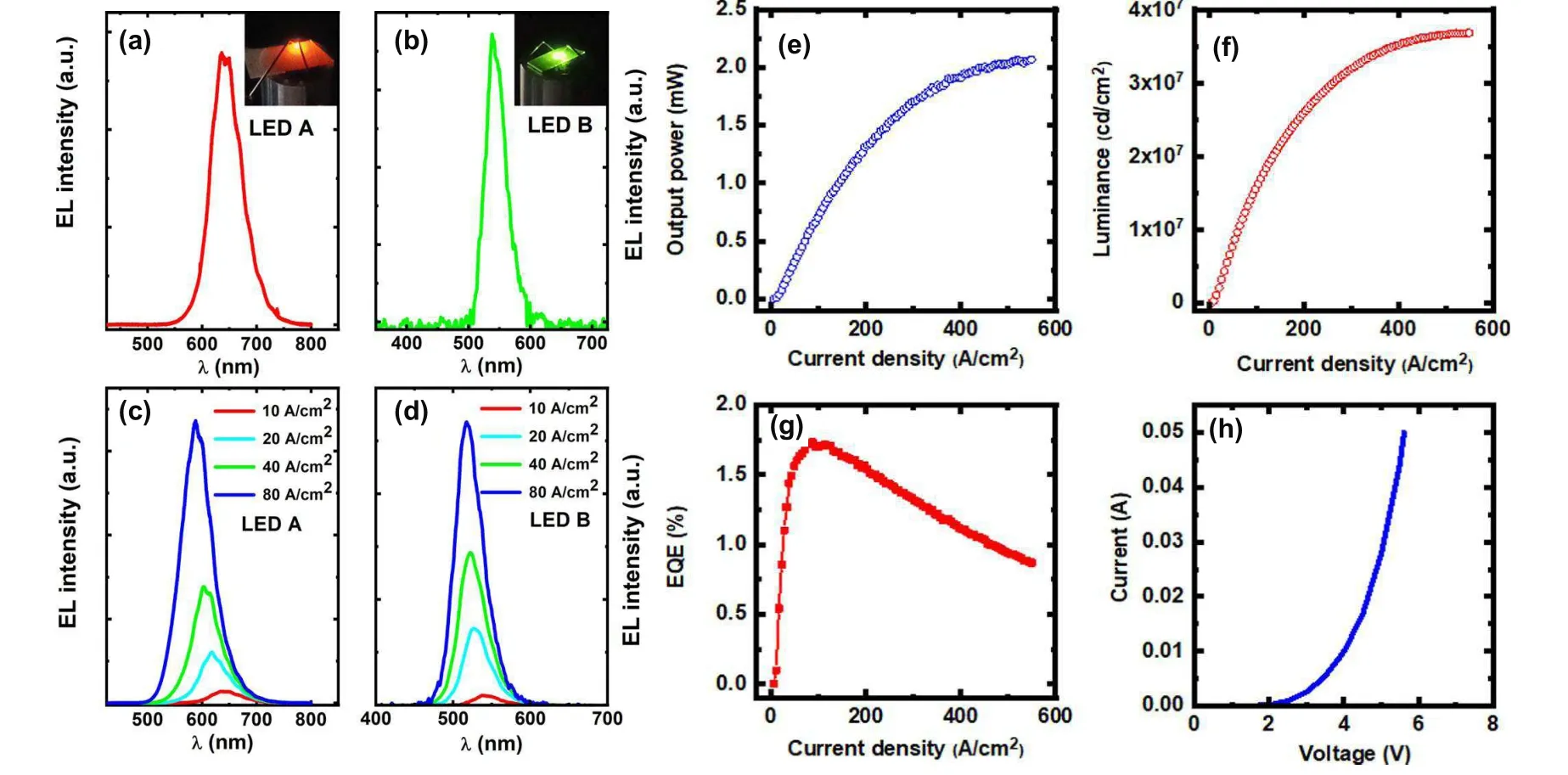
Fig.4. EL spectra at 10 A/cm2 for(a)overgrown μLED arrays(LED A)and(b)planar reference(LED B)and insets are emission images. EL spectra with increased current densities from 10 A/cm2 to 80 A/cm2 for(c)LED A and(d)LED B,respectively;(e)light output power,(f)luminance,(g)EQE,and (h) current–voltage characteristics of the μLED array device (LED A). Reprinted with permission from Ref. [36]. Copyright 2022 American Chemical Society(https://creativecommons.org/licenses/by/4.0/).

Fig.5. (a)Forward I–V characteristics of three overgrown μLEDs(diameter: 3.6 μm,5 μm and 40 μm); (b)reverse leakage current; (c)I–V characteristics for μLEDs with conventional etching methods;(d)and(e)capacitance comparison of overgrown μLEDs and mesa-etched ones;(f)and(g)RC constants comparison between overgrown μLEDs and mesa-etched ones. Reprinted with permission from Ref. [37]. Copyright 2021 Phys. Status Solidi A/Wiley-VCH(https://creativecommons.org/licenses/by/4.0/).
3.2.4. Demonstration of μLEDs with reduced leakage current
Leakage current is a particularly serious issue for μLEDs,as it often generates an unintentional switch-on of pixels in practical applications. Many reasons can cause leakage current including surface recombination and sidewall damage induced as a result of dry etching. Of course,it also leads to reduced luminous efficiency. Our direct epitaxial approach does not suffer from side wall damages, leading to a great potential to reduce the reverse leakage current. To confirm this,a comparative measurement using LCR meter and Keithley power source has been carried out to investigate the current–voltage(I–V)and capacitance–voltage(C–V)performances of the μLEDs fabricated using a conventional dry etching approach and our direct epitaxial approach. By measuring the leakage current of the μLEDs achieved by our direct approach,it was found that the leakage current per μLED and the leakage current dispersion are smaller than those of the conventionally mesa-etched μLEDs. With reducing the size of μLEDs,leakage current increases due to an increased perimeter to area ratio and corresponding larger surface recombination rate.Reduced leakage current can ensure high luminous efficiency with scaling down μLED size. By measuring capacitance–voltage behaviors, it was found that both operational voltage and RC constants show more favorable to the devices obtained by using our direct epitaxial approach than the conventionally mesa-etched μLEDs[37]as shown in Fig.5.This feature makes the μLEDs obtained using our direct epitaxial approach suitable for high-speed switching applications such as VLC.
4. Demonstration of a monolithic integration of μLEDs with HEMTs for microdisplay and VLC
Microdisplay can only work with its electronic driving parts. Therefore,it is also important to integrate μLEDs with its electronic driving circuits. Currently, a heterogeneous integration approach is widely adopted, such as wafer-to-wafer bonding to integrate μLED display with CMOS circuits for AR applications and mass transfer (laser lift-off, pick and place, etc.) to integrate μLED chips with TFT backplane for TV applications. However, high cost, low yield and poor assembly efficiency are still hindering these techniques being employed in massive production.
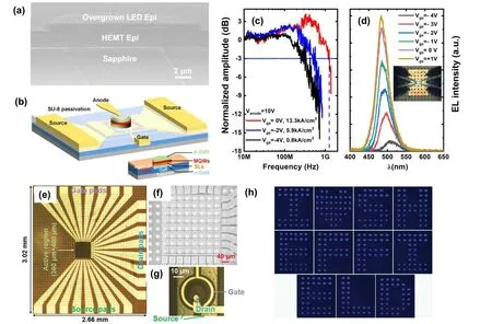
Fig.6. (a) A cross-sectional SEM image and (b) schematic illustration of single monolithic HEMT-μLED device; (c) 3 dB bandwidth and (d) EL spectra of integrated devices;[38] (e)8×8 HEMT-μLED arrays as a display chip;(f)an SEM image of active region and(g)a single pixel microscopic image and(h)displayed images. Reprinted with permission from Ref.[38]Copyright 2021 American Chemical Society and Ref.[39]2021 Advanced Materials Technologies/Wiley-VCH(https://creativecommons.org/licenses/by/4.0/).
In contrast,our direct epitaxial approach can also enable a monolithic integration of μLEDs with HEMTs. Traditional selective overgrowth method suffers from etching damage to LEDs and largely an increased growth rate near the boundary between mask covered region and overgrowth region.[44–48]Here,in our approach,a proper design in growth parameter ensures a uniform growth rate across the whole region,thus leading to smooth surface of μLEDs. For our direct epitaxy approach,there is no etching process involved,eliminating dryetching induced damages on the sidewalls of μLEDs.By using our direct epitaxial approach on a HEMT template, we have successfully demonstrated a monolithic HEMT-μLED device(where the μLEDs diameter is 20 μm)with a 1.2 GHz 3 dBbandwidth as shown in Figs.6(a)–6(d),[38]the highest one reported for c-plane III-nitride LEDs.[49]
Furthermore, an 8×8 monolithically integrated HEMTμLED arrays have been achieved[39]as shown in Figs. 6(e)–6(h), demonstrating a new concept for microdisplay applications. Such a monolithic integration scheme avoids the great difficulty in employing either the widely used mass transfer approach or the pick-and-place method for assembly.
5. Conclusion and perspectives
In summary, a confined selective epitaxy approach to achieving μLEDs has been developed by the Sheffield team,featuring many major advantages such as ultrahigh external quantum efficiency, stable emission color, enhanced indium incorporation to achieve red emissions, low leakage current and parasitic capacitance, and great potential to be integrated with electronic devices. All these advantages make this approach a promising candidate to fabricate high quality μLEDs for microdisplay and VLC applications.
Acknowledgment
Project supported by the Engineering and Physical Sciences Research Council (EPSRC), U.K., via EP/P006973/1,EP/T013001/1,and EP/M015181/1.
猜你喜欢
——王涛
杂志排行
Chinese Physics B的其它文章
- LAMOST medium-resolution spectroscopic survey of binarity and exotic star(LAMOST-MRS-B):Observation strategy and target selection
- Vertex centrality of complex networks based on joint nonnegative matrix factorization and graph embedding
- A novel lattice model integrating the cooperative deviation of density and optimal flux under V2X environment
- Effect of a static pedestrian as an exit obstacle on evacuation
- Chiral lateral optical force near plasmonic ring induced by Laguerre–Gaussian beam
- Adsorption dynamics of double-stranded DNA on a graphene oxide surface with both large unoxidized and oxidized regions