The application of a helicon plasma source in reactive sputter deposition of tungsten nitride thin films
2022-07-13YanYANG杨燕PeiyuJI季佩宇MaoyangLI李茂洋YaoweiYU余耀伟JianjunHUANG黄建军BinYU于斌XuemeiWU吴雪梅andTianyuanHUANG黄天源
Yan YANG (杨燕),Peiyu JI (季佩宇),Maoyang LI (李茂洋),Yaowei YU(余耀伟),Jianjun HUANG(黄建军),Bin YU(于斌),Xuemei WU(吴雪梅) and Tianyuan HUANG (黄天源)
1 College of Physics and Optoelectronic Engineering,Shenzhen University,Shenzhen 518060,People’s Republic of China
2 Key Laboratory of Optoelectronic Devices and Systems of Ministry of Education and Guangdong Province,College of Physics and Optoelectronic Engineering,Shenzhen University,Shenzhen 518060,People’s Republic of China
3 Advanced Energy Research Center,Shenzhen University,Shenzhen 518060,People’s Republic of China
4 School of Optoelectronic Science and Engineering,Soochow University,Suzhou 215123,People’s Republic of China
5 School of Physical Science and Technology,Soochow University,Suzhou 215123,People’s Republic of China
6 Institute of Plasma Physics,Chinese Academy of Sciences,Hefei 230031,People’s Republic of China
Abstract A reactive helicon wave plasma(HWP)sputtering method is used for the deposition of tungsten nitride(WNx)thin films.N2 is introduced downstream in the diffusion chamber.The impacts of N2 on the Ar-HWP parameters,such as ion energy distribution functions (IEDFs),electron energy probability functions (EEPFs),electron temperature (Te) and density (ne),are investigated.With the addition of N2,a decrease in electron density is observed due to the dissociative recombination of electrons withThe similar IEDF curves of Ar+ andindicate that the majority ofstems from the charge transfer in the collision between Ar+and N2.Moreover,due to the collisions between electrons and N2 ions,EEPFs show a relatively lower Te with a depletion in the high-energy tail.With increasing negative bias from 50 to 200 V,a phase transition from hexagonal WN to fcc-WN0.5 is observed,together with an increase in the deposition rate and roughness.
Keywords: helicon wave plasma,reactive sputtering,tungsten nitride,plasma diagnosis
1.Introduction
Among the various gaseous state coating techniques,costeffective reactive sputtering methods are suitable for the deposition of wide-area thin films with high rates and tunable compositions [1].Reactive sputtering has significant industrial and commercial relevance,as a variety of compound coatings can be synthesized using a metal target with the addition of reactive gas (e.g.N2,O2and CH4).For example,transition metal nitride thin films,such as TiNx,CrNxand WNx,with excellent hardness,can be used as wear-resistant protective coatings on cutting tools [2-4],and transparent conducting oxide (TCO) thin films,such as InOxand ZnOx,with high light transmission rates and low resistivity,can be applied in flat panel displays,solar cells and light emitting diodes [5,6].However,for commonly used reactive magnetron sputtering,several serious problems exist; for example,the low target utilization due to the deep and narrow erosion trench[7],and the‘poisoning’effect ascribed to the formation of the compound layer[8,9].Moreover,the re-sputtering and the surface damage resulting from the high-energy sputtering particles are also urgent problems that need to be solved[10].
To overcome these inadequacies,a surface-damage-free reactive sputtering deposition technique is proposed based on the source.A helicon wave is a circularly polarized whistler wave propagating along magnetic field lines [11].A helicon wave plasma (HWP) source can excite a plasma beam with high density (>1018m-3) and low electron temperature (<10 eV) under extremely high vacuum (~10-2Pa in the deposition chamber) [12].Also,as the antenna is wrapped around the source tube,the pollution due to the erosion of the antenna material can be avoided.Moreover,as a ‘remote source’,the flux and energy of the ion beam toward the target can be controlled independently by tuning the radio frequency power and the bias voltage.Moreover,the beam uniformity can be modified by tuning the magnetic field geometry [13].With these merits,the HWP reactive sputtering technique has been used for the synthesis of TCO (e.g.TiOxand ZnOx)coatings [14,15],dielectric SiOx/ZrOxdistributed Bragg reflectors [16] and WNxhard coatings [17].In HWP sputter deposition,the properties,crystallization and morphology can be well tailored by tuning the discharge parameters.In general,the film thickness depends on the ion flux and energy,the stoichiometry ratio x depends on the partial pressure of the reactive gas and the crystallinity mainly depends on the substrate temperature.Nevertheless,most of these research studies remain quasi-empirical and statistical.The mechanism of reactive HWP sputtering has not been fully understood:for instance,the ionization and dissociation processes of seeded reactive gases,which provide the raw particles for the cluster nucleation,and the effects of seeded reactive gases on the plasma beam parameters,which are crucial for target sputtering,such as ion energy and flux.
In this work,a steady-state Ar-HWP beam is excited in the High Magnetic field Helicon eXperiment (HMHX)device.To understand the interaction processes between N2and Ar-HWP,the ion and free electron properties,such as the ion energy distribution function (IEDF),electron energy probability function (EEPF),electron density and temperature,are investigated before and after N2seeding.WNxfilms are successfully prepared on 304 stainless steel substrates with various target bias voltages,which will be further applied as deuterium diffusion barriers due to their low sputtering yield and deuterium (D) retention [18].The crystalline phase,composition and morphology of the films have been characterized.In section 2,the experimental procedure is presented.In section 3,the results are discussed in detail and the conclusions are given in section 4.
2.Experimental procedure

Figure 1.A schematic of the experimental setup for WNx deposition.
The HMHX device used for the synthesis of WNxfilms has been described in detail elsewhere [17,19].As shown in figure 1,HWP is excited in a remote aluminum oxide tube by a right helical antenna at a frequency of 13.56 MHz.Then,it is spread along the magnetic field toward the W target(50 mm×50 mm×10 mm,99.97%) in the diffusion chamber,where pure N2(99.999%) is seeded through the annular-flow nozzle.The flow rate of the Ar (99.999%)flowing into the source tube is fixed at 50 sccm and the flow rate of N2seeding downstream is fixed at 30 sccm.Before operation,the typical base pressure was evacuated to 5×10⁻⁵Pa.An adjustable negative bias Vtis applied on the target for the acceleration of cations.Stainless steel substrates(4 mm×4 mm×1 mm) are mounted on the floating alumina ceramic substrate holder in front of the target.The axial distance between substrates and the target surface is fixed at 1.5 cm.Before being mounted,the substrates are sequentially cleaned in an ultrasonic bath using acetone,ethyl alcohol and deionized water.WNxfilm deposition is carried out at radio frequency power of 1 kW with a permanent axial magnetic field of 1300 G for 30 min at room temperature.
For plasma diagnoses,the Hiden (ESPION) Langmuir probe is mounted at 2 cm in front of the target surface to determine the EEPFs,electron density (ne) and temperature(Te).A Hiden electrostatic quadrupole plasma(EQP)detector(Series 1000) is used to observe the composition and the energy of ions incident on the target surface.During measurements,the target is removed and the orifice of the EQP detector is placed precisely at the target location.For film characterizations,θ-2θ X-ray diffraction (XRD) scans are performed using a Bruker D8 ADVANCE diffractometer with a Cu Kα line at 0.15418 nm as a source,which provides the crystalline structure information.The surface topography together with the chemical elemental composition is analyzed using a Dimension Icon atomic force microscope (AFM) in tapping mode and scanning electron microscopy (SEM,Hitachi SU-8010) equipped with a Bruker XFlash 6130 energy dispersive X-ray spectroscopy (EDS) system.
3.Results and discussion
3.1.Plasma diagnostics
The typical ion mass spectra measured by the EQP detector in‘+ ion’ mode near the target during Ar-HWP discharge with and without N2seeding are plotted in figure 2.For pure Ar-HWP discharge,the major ions are atomic Ar ions(Ar+)with the peak at amu 40.As N2is injected,as well as Ar+ions,atomic N ions (N+) and N molecular ions,can also be observed,with peaks at amu 14 and 28,respectively.

Figure 2.Typical ion mass spectra from the near target region measured by an EQP detector with N2 seeding; the insert shows the spectra for pure Ar HWP.
As shown in figure 3(a),without N2injection,the IEDFs of Ar+present a typically bimodal distribution.The mean ion energy for the first peak is 10.9 eV,which can be attributed to the local plasma potential.Furthermore,an ion beam can be identified by the second peak,with higher mean ion energy at about 31.5 eV.The beam energy can be obtained from the energy difference between these two peaks,which is about 20.6 eV [20].The ion beam stems from the electrostatic acceleration through the current-free double-layer (CFDL)structure.The CFDL structure downstream in the HWP beam is caused by the expanding magnetic field and vessel geometry near the throat of the diffusion chamber [21].
In figure 3(b),it is found that,as N2is injected,the IEDF curve of thecoincides well with that of the Ar+.Thus,we can speculate that the majority of theions are formed not by electron impact ionization but by the charge-transfer processes in collisions between Ar+and N2(Ar++N2=Ar+since their ionization energies are close(15.8 eV for Ar+and 15.6 eV for N2)[22].In addition,with the absence of N+,a fraction of themay originate from the charge transf er between N+and N2(N++N2=N+The IEDF curve of the N+also presents a bimodal structure.Thus,most of the N+ions may originate from the dissociative charge transfer of Ar+with N2(Ar++N2=N++N+Ar),while a small number of N+ions may also be produced by the reaction ofwith N2+N2=N++N+N2).According to the research by Shahin[23],for a glow discharge in a mixture of Ar/N2,as the average ion energy increases,theyield does not change much,while the N+yield increases rapidly.Thereby,a remarkable rise in the intensity can be expected in the high-energy tail of the N+IEDFs.
In figure 4(a),the electron density nemeasured by the Langmuir probe as a function of the radial position is plotted for both pure Ar and with N2seeding.The distribution shows a typical ‘center-peaked’structure with a peak value at about 2.7 ×10¹⁹m-3.The high-efficiency center heating mechanism for the HWP is uncertain.A commonly accepted theory ascribes it to the bulk mode conversion from a helicon wave to a Trivelpiece-Gould (TG) wave,which is suitable for thepower deposition due to the shorter wavelength [24].As N2is added,a significant fall in the electron density can be observed with the center density at5.5 ×1018m-3.To explain this phenomenon,the fundamental electron/Ninvolved interaction processes and relevant rate constants are listed below in table 1.The rate constants of processes(1)-(6)are quoted from [25].They are closely related to the electron temperature Te,which can be drawn from the EEPF in figure 4(b).Here,the temperature for the bulk electrons is used at 3.3 eV.For process(6),the rate constant is also related to the mean ionic energy ofIt can be drawn from the IEDF in figure 3(b) at about 14.6 eV.Thereby,the rate constant k for process (6) can be calculated,which is 5.9×10⁻⁷cm3s-1.It is obvious that among these interaction processes,the consumption of the electrons only occurs in process (6).Also,the rate constant for process (6) is much higher than those for other processes.Thereby,the decline of the electron density should be attributed to the dissociative recombination of electrons with(e+→N+N).
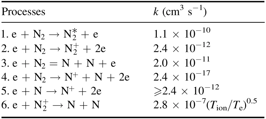
Table 1.Important interaction processes involving electrons in Ar-HWP discharge with N2 seeding.Here,the rate constant k is quoted from [25].
EEPFs measured at 2 cm in front of the target and r=0 cm are shown in figure 4(b) for both pure Ar HWP and with N2seeding.In the pure Ar discharge,the EEPF presents a typical Maxwellian distribution with a temperature at 4.5 eV.As N2is added,a lower bulk electron temperature at 3.3 eV can be observed.Moreover,the EEPF presents a depletion of the high-energy tail (1.6 eV) compared to the Maxwellian distribution fitting to the low-energy region (3.3 eV).The turning point where the depletion starts is about 20 eV.It matches well with the peak of the total scattering cross sections for the e-N2collisions,which is also located near 20 eV [26].In this case,with N2seeding,the fall in the bulk electron temperature and the depletion of the high-energy electrons can be attributed to the energy loss during e-N2collisions.
The vibration temperature (Tv) of N2is also important for gas discharge because vibration excitation with adiabatic properties can trap and store energy,which is crucial for chemical reactions in plasma.Characteristic optical emission spectra for Ar helicon plasma with seeding N2at FN2=30 sccm are shown in figure 5,where the typical spectrum of a N2second positive system (SPS) is clearly discernible.The Tvof N2can be calculated by fitting the N2SPS (C3Πu→B3Πg) spectra peaks (N2SPS(0,2)at 380.5 nm and N2SPS(1,3)at 375.5 nm)with the measured spectra using a widely used simulation method,which has been described in previous works [27,28].

Figure 3.IEDFs of the major ions (Ar+,N+ and) near the target for HWP operating with (a) pure Ar and (b) with N2 seeding.

Figure 4.(a)Radial distribution of the electron density ne,and(b)EEPFs(r=0 cm)for pure Ar and with N2 seeding.The Langmuir probe is located at 2 cm in front of the target.
As shown in the illustration of figure 5,a decrease in vibrational temperature from 4970 to 4490 K can be observed with the increasing N2flow rate from 5 to 30 sccm.The vibration temperature Tvis related to the density and temperature of the excitation particles in the plasma[29].With the increase in the N percentage in the discharge,the populations of electrons and Ar metastable states both decrease,and the probabilities of electron impact and Penning excitation also decrease correspondingly.This is why the vibrational temperature of N2decreases with the addition of N to Ar plasma.
3.2.Deposition of WNx films
In this section,WNxfilms grown on the 304 stainless steel substrates at room temperature with various negative bias voltages(50-200 V)are investigated.In table 2,the [N]/[W]stoichiometry ratio measured by EDS,the growth rate evaluated by the film thickness and the root mean square (RMS)roughness obtained from the AFM are listed.Moreover,the crystallinity of the films can be determined from the ratio of the area of the crystalline peaks and the area of all the peaks(amorphous and crystalline) from the XRD spectra [30].
The target collected current (I)and the W sputtering rate(δ) estimated by the target weight loss are shown in figure 6.For the target with a negative bias voltage,as the electron is retarded,the majority of the current belongs to the ion current Iionand the ion-induced secondary electron current Isec.Thereby,the rising current with increasing bias voltage may result from both the expanding target sheath and the increasing Isec.Unlike the current,δ shows a sharp increase with the bias voltage,because a higher bias voltage can effectively improve the sputtering yield of Ar+→W [31]and N+/→W [32].This variation trend matches well with the deposition rate in table 2.
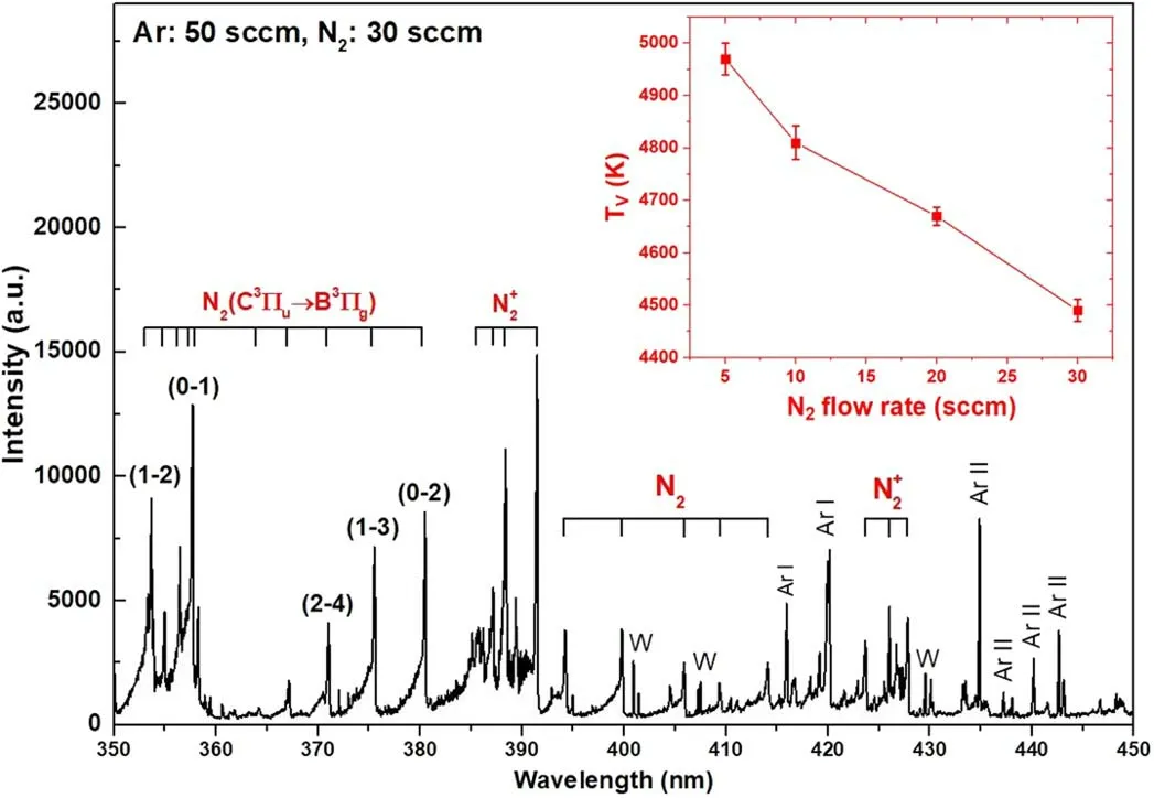
Figure 5.Characteristic spectra of Ar-helicon plasma with seeding N2 at 30 sccm.The illustration shows the vibrational temperature Tv as a function of the seeding N2 flow rate.
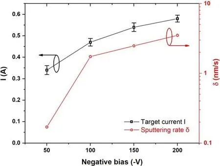
Figure 6.The target current I and sputtering rate δ as functions of the negative biases.
In figure 7,typical XRD results for WNxfilms grown on the 304 stainless steel substrates with negative bias ranging from 50 to 200 V are plotted.The spectrum for the substrate is also presented.For the low bias voltage at 50 V,the[N]/[W]stoichiometry ratio is about 1.08 and a weak peak at 2θ=35.68° can be detected,which can be ascribed to the(100) plane of the hexagonal WN phase (JCPDS 25-1256).The low crystallinity at 7.8% with a relatively weak hexagonal WN signal and a strong substrate signal indicates that,due to the low sputtering rate,the growth of the WN crystallites is inhibited under a relatively low growth rate at 1.3 nm min-1.For the higher bias voltage at 100 V,with the increase in the deposition rate to 9.3 nm min-1,the WN(100)peak becomes stronger with a higher crystallinity at 52.4%,together with the appearance of the hexagonal WN(110)peak at 2θ of 63.04° (JCPDS 25-1256).When we further increase the bias voltage to 150 V,with a lower x=0.87,the WN(100) and (110) diffraction peaks become sharper with a substantial rise in the intensity,indicating a high crystallinity(81.0%).Also,a face-centered cubic β-WN0.5phase can be detected by the deconvolution procedure of the broad peak near 73.32°.This peak located at 2θ=74.06° is associated with the β-WN0.5(311) reflection (JCPDS 25-1257).As the bias voltage increases to 200 V,the [N]/[W] stoichiometry ratio x drops to 0.63 and the film presents a typical NaCl-type β-WN0.5phase with identifiable peaks at 2θ=36.04°,42.14°,60.84° and 72.58°,which correspond to the (111),(200),(220) and (311) reflections,respectively.However,compared with the standard values,a left shift of the characteristic peaks can be observed,which could be attributed to the expansion of the lattices with the excess interstitial N atoms [33].This phase evolution from hexagonal WN to β-WN0.5can be ascribed to the increased density ratio of W to N in the reactive background plasma cloud with a higher W sputtering rate.Moreover,the appearance of the amorphous peaks to some extent causes a decrease in the crystallinity from 81.0% to 73.8%.

Figure 7.XRD spectra of WNx films deposited with various negative biases.The black line corresponds to the 304 stainless steel substrates without coatings.

Figure 8.SEM photographs of WNx films deposited on 304 stainless steel substrates with different negative biases at (a) 50 V,(b) 100 V,(c) 150 V and (d) 200 V.

Table 2.The [N]/[W] stoichiometry ratio,growth rate,RMS roughness and crystallinity of the WNx films deposited with various negative bias voltages from 50 to 200 V.
The SEM micrographs (50000× magnification) of the WNxfilms deposited on the 304 stainless steel substrates with various negative biases from 50 to 200 V are shown in figure 8.At 50 V,due to the low sputtered W flux,a relatively loose structure with sparsely distributed bumps is formed.When the negative bias increases to 100 V,the graph shows that the deposited thin film consists of scale-like irregular shaped grains with an average size around 75±10 nm.When we further increase the bias voltage to 150 V,a finer grain structure can be observed as the hexagonal WN is mixed with a small amount of β-WN0.5[34].For higher bias at 200 V,the morphology patterns become denser with a larger average size of the conglomerated coarse grain.With the increment of the W density in the plasma,WNxcrystallites will be more agglomerated in the process of deposition.In this case,the RMS roughness of the WNxfilms also increases with increasing bias voltage.
4.Summary and conclusion
In this work,sputter deposition of WNxfilms has been performed using helicon-excited Ar plasma with N2seeding.The ionization and dissociation mechanisms of seeded N2together with the role it plays in film synthesis are carefully investigated using plasma diagnoses and film characterizations.
With the injection of N2,the ion mass spectrum confirms the existence of bothand N+.Most of theand N+ions are generated by the charge-transfer collision (Ar++N2=Ar+) and the dissociative charge-transfer (Ar++N2=N++N+Ar) processes,respectively.Moreover,a significant decrease in the electron density can also be detected with N2seeding,which can be attributed to the dissociative recombination of electrons with(e+→N+N).In addition,the EEPFs show a depletion of the high-energy electrons due to the e-N2collisions.WNxthin films have been successfully deposited on the stainless steel substrates at room temperature.With increasing negative biases from 50 to 200 V,a phase evolution of hexagonal WN to fcc-WN0.5can be observed due to the increasing W sputtering rate.Also,with the increment of the W content in the plasma,the structure becomes denser with a significant increase in the average grain size.
This work gives us an in-depth understanding of the interactions between Ar HWP and injected N2.It can help us trace the sources of N atoms and atomic ions(N+)which are essential for the nucleation of WNx.On the other hand,based on the HWP source,this work presents an innovative reactive sputtering deposition method for the synthesis of WNxthin films with a high growth rate (up to 25.8 nm min-1) and controllable elemental compositions.However,this work is still in the early stages; further efforts are needed to improve the crystallinity,uniformity and adhesion of the WNxfilms deposited on the stainless steel substrates.
Acknowledgments
This work is supported by National Natural Science Foundation of China (Nos.11975163,12175160) and Shenzhen Clean Energy Research Institute.
猜你喜欢
杂志排行

Plasma Science and Technology的其它文章
- Investigation on the multi-hole directional coupler for power measurement of the J-TEXT ECRH system
- Neutronic analysis of Indian helium-cooled solid breeder tritium breeding module for testing in ITER
- Investigation on the electrode surface roughness effects on a repetitive selfbreakdown gas switch
- Roll-to-roll fabrication of large-scale polyorgansiloxane thin film with high flexibility and ultra-efficient atomic oxygen resistance
- Effect of shock wave formation on propellant ignition in capillary discharge
- Machine learning-based method to adjust electron anomalous conductivity profile to experimentally measured operating parameters of Hall thruster