Spin transport in epitaxial Fe3O4/GaAs lateral structured devices
2022-06-29ZhaocongHuang黄兆聪WenqingLiu刘文卿JianLiang梁健QingjieGuo郭庆杰YaZhai翟亚andYongbingXu徐永兵
Zhaocong Huang(黄兆聪) Wenqing Liu(刘文卿) Jian Liang(梁健)Qingjie Guo(郭庆杰) Ya Zhai(翟亚) and Yongbing Xu(徐永兵)
1School of Physics,Southeast University,Nanjing 211189,China
2Spintronics and Nanodevice Laboratory,Department of Electronics,University of York,York YO10 5DD,United Kingdom
3York-Nanjing Joint Center in Spintronics,School of Electronic Science and Engineering,Nanjing University,Nanjing 210023,China
4Department of Electronic Engineering,Royal Holloway University of London,Egham,Surrey TW20 0EX,United Kingdom
Keywords: spin field-effect transistor,spin injection and detection,half metal,magnetoresistance
1. Introduction
The spin transport and the spin manipulation of carrier spins represent two key elements of semiconductor(SC) spintronics logic devices including several viable types of spin transistors, particularly spin field-effect transistors(FETs).[1–3]Research on spin injection and detection and spin coherence in semiconductors continues to draw extensive interest from both the scientific and the technical communities.[4–6]The electron spin relaxation time in SCs has been revealed to be several orders of magnitude longer than the electron momentum and energy relaxation times.[7]Further experimental evidence has been proven that electrons can be transported a distance of as large as 100 μm without loss of their spin coherence using an electric field for the case of GaAs.[8]These observations suggest that spin information could be transmitted efficiently in specific SC channels.Although all electrical spin field effect transistors have been demonstrated, they operate at low temperatures and require multi-terminals or non-local geometry.[9–14]It has been predicted that the magnetoresistance(MR)effect due to diffusive electron transport may exist in a two-terminal spin-valve structure with a non-magnetic SC layer.[15,16]However,room temperature spin injection and transmission in FM/SC/FM system(FM:ferromagnet)is still challenging.
Ferromagnetic source with high spin polarization near the Fermi level has inherent advantages in spin injection. Half metallic Fe3O4film in this regard is an ideal candidate due to its high Curie temperature of 858 K and large spin polarization near 100%at the Fermi level at room temperature,even though a reduction of spin polarization of Fe3O4may appear due to non-stoichiometry or surface effect.[17–20]Unlike ferromagnetic metals and alloys that have a significant ‘conductivity mismatch’[21–24]with the SCs,[25]Fe3O4has relatively high electrical conductivity and potentially forms non-ohmic contact with SCs like GaAs.[26,27]Moreover,spin–orbit coupling(SOC)also play an important role in spin FET devices.[1,3,28]In this respect, the enhanced SOC effect near Fe3O4/GaAs interface[29]and two-dimensional (2D) SC as the spin transport media due to effects from 2D confinement are preference for the spin FET device. In this article,we report the fabrication and characterizations of a two-terminal lateral Fe3O4/ndoped GaAs(100) thin layer/Fe3O4spin-valve (SV) device.The bias-dependent room-temperature MR effect is observed,which demonstrates the all-electric spin injection and detection from a magnetic half-metal to a semiconductor at room temperatures.
2. Experiments
Firstly,an ultrathin Fe3O4film was epitaxially grown on a GaAs(100)substrate. The GaAs(100)wafer used in this study consisted of epilayers of n-GaAs with the following structure:amorphous As-cap/n-GaAs (500 nm, 3×1018cm-3)/500 μm thick semi-insulating(S.I.)GaAs(100). After cleaned in acetone and IPA thoroughly,GaAs wafer was loaded into a UHVMBE chamber with a base pressure of 2×10⁻¹⁰mbar and annealed at 830 K for 30 min to desorb the capped As layer and form a smooth single crystalline GaAs surface. By using the postgrowth oxidation method,[30]a thickness of 4 nm Fe film was deposited on top of the GaAs wafer at a chamber pressure better than 1×10⁻⁹mbar at room temperature,using e-beam evaporator at a rate of 2 °A/min, followed by oxidizing in an oxygen environment of 5×10⁻⁵mbar for 10 min at 500 K.The growth process of the single crystalline magnetite film was monitored by reflection high-energy electron diffraction(RHEED).The RHEED patterns of Fe3O4film along the GaAs[0¯11]axis is shown in Fig.1(a),which suggests the epitaxial growth.
A local geometry with four contacts is used to measure the spin signal of the lateral spin valve structure, as schematically shown in Fig. 1(b). Subsequently, two Fe3O4electrodes (Fe3O41: 17×156 μm, Fe3O42: 97×156 μm) with an edge to edge distance of 2.6 μm were patterned by the electron beam lithography, optical lithography and selective H2SO4-based etchant. The scanning electron microscope image of two Fe3O4electrodes is shown in Fig. 1(c). Finally,four Au electrodes were fabricated by optical lithography and lift-off process. The total fabrication process of the Fe3O4/n-GaAs/Fe3O4spin valve device is summarized in Fig. 1(d).Subsequently,all terminals are wire bonded to a chip and connected to Keithley Source Meter 2450 for magnetic transport measurements.

Fig. 1. (a) RHEED patterns of Fe3O4 with the electron beam along GaAs(100)[0¯11] direction. (b) Schematic diagram of the two-terminal lateral device. (c)Typical SEM image of the fabricated Fe3O4/GaAs/Fe3O4 device. (d)Illustration of the fabrication process of the device.
3. Results and discussion
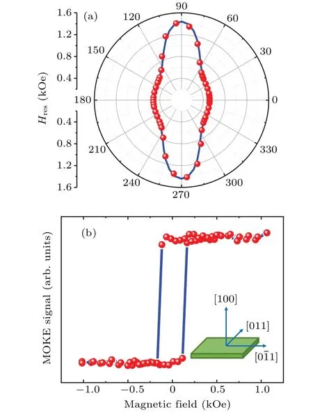
The in-plane magnetic anisotropy of Fe3O4/GaAs film obtained by ferromagnetic resonance is shown in Fig. 2(a).It is seen that the film shows a dominant uniaxial symmetry with its easy axis(EA)along[0¯11](φH=0°). An additional small four-fold symmetry is observed clearly with its EA along[010] and [001](φH=45°and 135°, respectively), which reveals a dominant uniaxial magnetic anisotropy(UMA)plus a minor cubic magnetic anisotropy in our ultrathin Fe3O4single crystal film. The UMA is induced by the GaAs substrate due to the interfacial effect between Fe3O4and GaAs,which may originate from the unidirectional chemical bonding and the anisotropic lattice relaxation, while the four-fold magnetic anisotropy originates from the cubic magnetocrystalline anisotropy of bulk Fe3O4.[31]By fitting the experimental angular dependence of the resonance field data with saturation magnetizationMs=470 Gs obtained by vibrating sample magnetometry(VSM),the UMA constant is determined as 5.7×10⁴erg/cm3and the magnetocrystalline anisotropy constant is determined as-3.1×10⁴erg/cm3, about 26% of the value of bulk Fe3O4(-11.8×10⁴erg/cm3)[32]due to the interfacial effect and the lattice relaxation at the Fe3O4/GaAs interface. The Kerr loop with the applied field along the EA of UMA(GaAs(100)[0¯11])direction is measured,as shown in Fig. 2(b). It shows a perfect square loop with the squareness of 96%and the coercivity of 130 Oe,which suggests that the EA of UMA direction is perfect for the magnetic electrode of the spin injection and detection device.
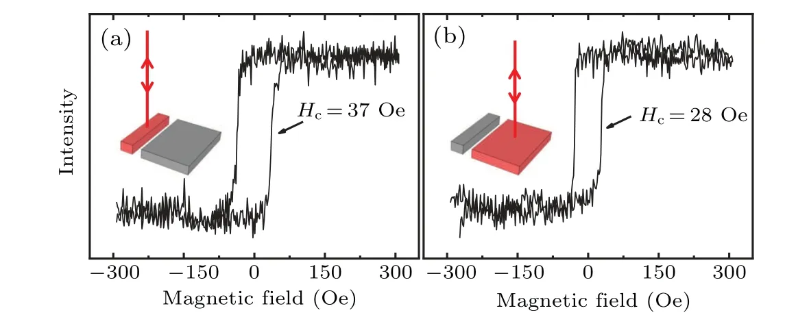
For fabricating the epitaxial Fe3O4/GaAs two-terminal devices,the long edges of the two Fe3O4electrodes are along EA of Fe3O4. The local spin valve (LSV) structure with a four-terminal setup was used to measure the spin transport effects of the device and the external magnetic field was applied in-plane to magnetize the Fe3O4electrodes(see Fig.1(c)). We intentionally induced shape anisotropy between the two Fe3O4electrodes,where the aspect ratios of two Fe3O4electrodes as 1:9 and 6:9 were chosen respectively. Combining with the strong interfacial UMA, a large difference in coercivity can be expected. To ascertain this, we measured the magnetic hysteresis loops of Fe3O41 and Fe3O42 at room temperature by focused magneto-optical Kerr effect(FMOKE)with a spot size less than 1 μm,which consists of a stabilized 5 mW continuous HeNe laser of 635 nm wavelength,a stack of focusing lenses and a nano-positioning stage,as shown in Fig.3. From the magnetic hysteresis loops, we can see both high squareness and sharp magnetization switching,and 37 Oe and 28 Oe of coercivity corresponding to Fe3O41 and Fe3O42 electrodes,respectively, can be distinguished, which are very important for further MR measurements.


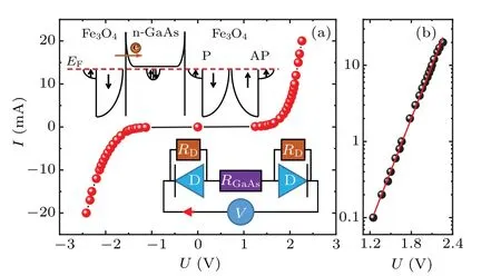
Figure 4(a) displays nonlinear and symmetric current–voltage(I–V)characteristics for the device. Here,the nonlinearity agrees with the expected non-Ohmic contacts between the n-GaAs layer and the Fe3O4electrodes, and the symmetricalI–Vcurve reveals that the barrier height between two Fe3O4electrodes and GaAs is nearly the same.[33]The working principle of the two-terminal SV device is elucidated using a simple electrical circuit,as shown in the inset of Fig.4(a).To take into account the Fe3O4/n-GaAs Schottky barriers in the actual device,[27]this circuit consists of two diodesD, each contributing a parallel resistance ofRDdue to potential diode imperfections. Since the two energy barriers are always oppositely biased, the diodes are assigned to connect back-toback in series with an additional resistanceRGaAs,given by the GaAs layer. By using the thermionic-field emission model,[34]the device currentI, which associates with the Schottky barrier heightφand the tunnelling parameter, can be defined asI=IS(eqV/βkT-1), whereIS=SAT2e-qφ/kT, andβandIScan be obtained from the logarithmic plot in Fig.4(b). Therefore, the barrier heights of the Fe3O41 and Fe3O42 contacts have also been determined as 0.36±0.02 eV, which agrees with our previous electrical characterization of Fe3O4/n-GaAs films.[26]

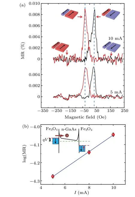
The device MR is performed with different applied currents at room temperature,and the magnetic field sweeps from-250 Oe to 250 Oe. The resistance of the spin valve device is around 390 Ω, and the signal-to-noise ratio is better than 5×10⁻⁶. With lineally fitting of the background of the raw data,the MR data with this background subtracted with different applied currents of 5 mA,8 mA and 10 mA are shown in Fig. 5(a). Here the MR is defined as MR=(RAP-RP)/RP,withRPandRAPbeing the device resistances at the parallel and antiparallel states, respectively. As the magnetic field sweeps, an obvious MR effect can be distinguished, which is largely different from our previous anisotropic magnetoresistance (AMR) on Fe3O4/GaAs film.[26]With a high magnetic field,Fe3O41 and Fe3O42 are in a spin parallel state,leading to a small resistance. The resistance reaches the maximum value near the applied field of 32±3 Oe,which is the average of coercivity of Fe3O41 and Fe3O42 electrodes,where Fe3O41 and Fe3O42 are in a spin antiparallel state.

Therefore, it can be inferred that the MR effect is originated from the two spin configurations of Fe3O41 and Fe3O42 electrodes, and the spin current is indeed injected from Fe3O41/Fe3O42 to n-GaAs layer and transferred through n-GaAs channel,and eventually detected by the other Fe3O42/Fe3O41 electrodes at room temperature. The switching of MR loop is slower than the MOKE result, which may originate from the tunnelling AMR.As increasing the applied current from 5 mA to 10 mA,the bias voltage increases and the MR ratio increases from 0.0053% to 0.0090%. The MR ratio accords logarithmic relationship with the applied current,as can be seen from Fig. 5(b), consistent with the tunnelling model, and the increase of bias voltage leads to the higher probability of tunnelling through the Schottky barrier. The inset of Fig.5(b)shows the schematic band structure of the device under biased conditions.When the bias voltage increases,the MR ratio increases,which is associated with an increased number of electrons from the injector contact tunnelling into the GaAs layer. Here, it can be deduced that the observed bias-dependent MR confirms the electrical spin injection and detection in our two-terminal SV device.
4. Conclusion and perspectives
In summary, we have demonstrated a bias-dependent spin injection and detection related MR effect in the twoterminal Fe3O4/n-GaAs(100)/Fe3O4lateral spin-valve device.The nonlinear and symmetric current–voltage(I–V)characteristic is observed for the device and the Schottky barrier height is calculated as 0.36 eV. The two Fe3O4electrodes along the magnetic easy axis of the film are fabricated to have different switching fields,which leads to clear MR effect at room temperature due to the parallel and anti-parallel alignments. The MR effect shows a strong bias dependence under different applied current, further confirming the spin injection across the Fe3O4/GaAs interface. Our work has demonstrated the feasibility in developing the room temperature two terminals lateral spin valve device without tunnelling spacer,which has potential applications for the high density spin FET devices.
Acknowledgements
Project supported by the National Key Research and Development Program of China(Grant No.2017YFA0204800),and the National Natural Science Foundation of China(Grant Nos.52071079 and 11504047).
杂志排行
Chinese Physics B的其它文章
- Ergodic stationary distribution of a stochastic rumor propagation model with general incidence function
- Most probable transition paths in eutrophicated lake ecosystem under Gaussian white noise and periodic force
- Local sum uncertainty relations for angular momentum operators of bipartite permutation symmetric systems
- Quantum algorithm for neighborhood preserving embedding
- Vortex chains induced by anisotropic spin–orbit coupling and magnetic field in spin-2 Bose–Einstein condensates
- Short-wave infrared continuous-variable quantum key distribution over satellite-to-submarine channels
