Signal modeling and impulse response shaping for semiconductor detectors
2022-06-18XueYuanWangJianBinZhouMingWangHuaiPingWangXuHongYiLiuPingHuang
Xue-Yuan Wang · Jian-Bin Zhou· Ming Wang· Huai-Ping Wang·Xu Hong· Yi Liu · Ping Huang
Abstract The output-signal models and impulse response shaping (IRS) functions of semiconductor detectors are important for establishing high-precision measurement systems. In this paper, an output-signal model for semiconductor detector systems is proposed. According to the proposed model, a multistage cascade deconvolution IRS algorithm was developed using the C-R inverse system,R-C inverse system, and differentiator system. The silicon drift detector signals acquired from the analog-to-digital converter were tested. The experimental results indicated that the shaped pulses obtained using the proposed model had no undershoot,and the average peak base width of the output shaped pulses was reduced by 36% compared with that for a simple model proposed in a previous work [1].Offline processing results indicated that compared with the traditional IRS algorithm, the average peak base width of the output shaped pulses obtained using the proposed algorithm was reduced by 11%, and the total elapsed time required for pulse shaping was reduced by 26%. The proposed algorithm avoids recursive calculation. If the sampling frequency of the digital system reaches 100 MHz, the proposed algorithm can be simplified to integer arithmetic. The proposed IRS algorithm can be applied to high-resolution energy spectrum analysis, highcounting rate energy spectrum correction, and coincidence and anti-coincidence measurements.
Keywords Output-signal model · Impulse response shaping·C-R inverse system·R-C inverse system·Integer arithmetic
1 Introduction
Semiconductor detectors are widely used for radiation measurements and nuclear analysis because of their high signal-to-noise ratios (SNRs) and high energy resolutions for rays and particles. Semiconductor detectors typically adopt reset-type charge-sensitive preamplifiers or R-C-type charge-sensitive preamplifiers.The semiconductor detector output is typically wide. In high-counting rate environments, the signals of semiconductor detectors accumulate significantly, resulting in counting loss and a low energy resolution. For coincidence measurements, it is necessary to obtain accurate time information of the signals. However, in high-counting rate environments, accurate time information of output signals is difficult to obtain,owing to large widths of the signals. For semiconductor detector systems, a high resolution and high counting rate are necessary for high-precision measurements. Digital pulse processing (DPP) systems are often adopted in semiconductor detector systems for signal processing and analysis[2]. Extensive research has been performed on digital systems for increasing the system resolution and counting rate.In research on digital systems,studies focusing on the output-signal model and the pulse-shaping algorithm have yielded interesting findings.
Output-signal models have been proposed for describing the pulse shape. They play an important role in pulse shaping. Nakhostin et al. described the peak value of the output voltage pulse as an exponentially growing signal with a single decay time constant [3]. Mohammadian-Behbahani et al. proposed a two-component biexponential model for characterizing the preamplifier output pulses generated by an NaI (Tl) detector [4]. Fo¨disch et al.developed a dual-exponential output-signal model with a single decay time constant for rectangular shaping [5].Bogova et al. described the input signal in the digital domain as the product of a single exponential function and a Heaviside step function [6]. Kantor et al. proposed a simple model with three time constants to describe the pulse shapes generated by radiation detectors [1]. Khilkevitch et al.presented an analytical formula with three time constants to describe the pulse shape caused by a gamma quantum in a scintillation detector [7]. However, these output-signal models were presented without detailed explanations and have not been extensively studied.
The impulse response shaping (IRS) algorithm is important for the development of high-precision measurement systems. Hong et al. proposed a unit IRS algorithm for counting-loss corrections in x-ray spectroscopy[8].Liu et al. presented a dual-exponential IRS algorithm for counting-loss correction in x-ray spectroscopy [9]. Jordanov et al. developed efficient recursive algorithms that allow real-time pulse-shaping [10]. Imperiale et al. discussed pulse-shaping algorithms for high-energy semiconductor gamma-ray spectrometry [11]. Zhao et al.designed a novel digital filter based on a sinusoidal function [12]. Abbene et al. applied the classical single-delay line-shaping technique to dead-time corrections[13].These algorithms are based on output-signal models with only one or two decay-time constants. The influence of outputsignal models with more time constants on these IRS algorithms has not been discussed.Thuraka et al.realized a recursive algorithm in a field-programmable gate array(FPGA) with minimum resources to synthesize a trapezoidal output pulse from a step-input pulse[14].Wen et al.proved that a pulse pile-up recovery algorithm based on template matching is effective for high-throughput gammaray spectroscopy [15]. Fernandes et al. developed a realtime algorithm for digitizer module FPGAs to calculate the amplitude of Gaussian-shaped pulses [16]. These digital solutions attempt to increase the resolutions and counting rates of semiconductor detector systems.However,they are based on complex mathematical operations and do not focus on the high-speed and parallel processing of realtime signals.
In this study,the signal characteristics of semiconductor detectors were analyzed, taking silicon drift detectors(SDDs) as an example, and a new output-signal model of the semiconductor detector system was established. The new output-signal model and the simple model proposed in[1] were tested with acquired signals of the SDDs. The results indicated that the new model more accurately reflected the output signals of the semiconductor detector system than the simple model. Traditional IRS algorithms based on Z-transforms are both complex and recursive.Recursion increases the complexity of DPP systems and imposes restrictions on the speed of pulse shaping. A nonrecursive multistage cascade deconvolution IRS (MCDIRS)algorithm based on the new model is proposed in this paper. The proposed algorithm avoids recursive calculation.The pipeline schemes of the direct-form finite impulse response (FIR) filter can be implemented using this algorithm. As the sampling frequency of the digital system reaches 100 MHz, the algorithm can be simplified to integer arithmetic, which is suitable for implementation using FPGAs. The proposed algorithm was tested and analyzed offline with the acquired SDD signals.The results indicated that the average peak base width of the output shaped pulses obtained using this algorithm and the total elapsed time required for pulse shaping were significantly reduced compared with those for the traditional algorithm.
The proposed output-signal model and IRS algorithm are important for the development of high-resolution energy spectrum measurement systems, coincidence measurement systems, anti-coincidence measurement systems,and high-counting rate correction systems.
2 Semiconductor detection system for nuclear radiation
A digital detection system usually includes a semiconductor detector, a preamplifier, a front-end circuit, an analog-to-digital converter (ADC), a digital-to-analog converter (DAC), a digital pulse processor, and computer software, as shown in Fig. 1.
SDDs, which were proposed in 1984 by Gatti and Rehak, are high-resolution position-sensitive detectors for fast-ionizing particles and x-rays. The function of SDDs is similar to that of Si-PIN photodetectors. However, the electrode structure of SDDs differs from that of Si-PIN photodetectors [17]. SDDs have excellent properties, such as a high sensitivity,a high energy resolution,a high count rate, low electronic noise, a low leakage current, a high quantum efficiency, and a low capacitance [18]. The capacitance of the output electrode of the SDD is <0.1 pF and is independent of the detector area. SDDs, which can be operated at room temperature without liquid nitrogen,are often used in x-ray analytical techniques, such as proton-induced x-ray emission, energy-dispersive x-ray spectroscopy, and x-ray fluorescence spectroscopy. They are the most commonly used detectors for x-ray spectroscopy.

Fig. 1 Typical block diagram of a digital detection system
The front-end circuit is usually composed of a C-R circuit, a linear amplifier, and an offset adjustor. The C-R circuit shapes the output signal of the detector to an exponentially decaying pulse.The linear amplifier changes the amplitude of the exponentially decaying pulse[8].The high-pass linear amplifier hardly changes the shape of the exponentially decaying pulse. The front-end circuit, which adopts high-pass linear amplifiers, can be simplified to a C-R circuit, which is referred to as the C-R system hereinafter. The amplified pulse is then sampled and quantized by the ADC, which follows the front-end circuit [19]. In most cases, the sampling frequency and quantization granularity significantly affect DPP. A digital pulse processor is generally composed of an FPGA and a microcontroller unit (MCU). The sampled pulse is processed in the FPGA and sent to the computer by the MCU.
3 Methods
3.1 Output-signal model for semiconductor detector systems
An output-signal model for semiconductor detector systems was developed by analyzing the output signals of the SDDs, preamplifiers, and C-R differential circuits.
3.1.1 Output signals of SDDs
In previous studies, the output signal of the chargesensitive preamplifier was generally approximated as a step signal or an exponentially growing signal with a single time constant, and the signal output by the SDD was approximated as an impulse signal or an exponentially decaying signal with a single time constant [19]. With the development of digital systems,the sampling rate has been increased by high-speed ADCs, the amount of noise in semiconductor detector systems has been reduced, and the precision of the sampling has been improved. The rise time of a nuclear pulse can be accurately detected and described. Our experimental results indicated that the output signals of the SDDs should be approximated as dual-exponential signals, as shown in Fig. 2a.
The dual-exponential signal is defined as follows:

where A represents the pulse amplitude, and τ2and τ3represent the falling and rising parts of the pulse,respectively.
3.1.2 Output signals of integral-reset-type charge
sensitive preamplifier
Charge-sensitive preamplifiers have low electronic noise,and the amplitudes of their output signals are hardly affected by parameters such as the interelectrode capacitance, open-loop input capacitance, and voltage gain. The preamplifiers adopted in high-resolution energy spectrum measurement systems are almost always charge-sensitive.Charge-sensitive preamplifiers include the resistancefeedback, direct-current (DC) optical-feedback, pulse optical-feedback, and integral-reset types. The circuit of the integral-reset-type charge-sensitive preamplifier used in digital systems is shown in Fig. 1.
The transformation of an input signal into an output signal by an integral-reset-type charge-sensitive preamplifier is mathematically described as a convolution of the input signal y1(t ) and the unit step function ε(t). The convolution is expressed as

Equation (2) can be rewritten as follows:

Fig. 2 (Color online) Simulations of signals output by the detector, preamplifier, and C-R system. a Simulation of the dual-exponential signal output by the SDD. b Simulation of the integral signal output by the preamplifier. c Simulation of the signal output by the C-R system

The output signal of the integral-reset-type charge-sensitive preamplifier is shown in Fig. 2b.
3.1.3 C-R convolution transform of signals
The charge collected by the integral-reset-type chargesensitive preamplifier increases with the accumulation of the detector output and DC bias, and it is not cleared until reset. The C-R differential circuit, as shown in Fig. 1, was adopted to process the output signal of the preamplifier.DC components were eliminated,and independent signals were obtained after the output signal was processed by the C-R differential circuit. The transfer function of the C-R differential circuit was obtained via analysis, where R and C are the resistance and capacitance values of RC circuit,respectively:

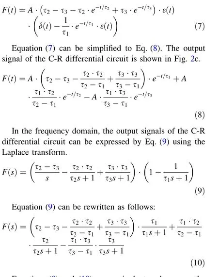
Equations (8) and (10) are equivalent and express the output signals of the C-R differential circuit in the time and frequency domains, respectively.
3.2 MCD-IRS algorithm
On the basis of the proposed output-signal model, an MCD-IRS algorithm is developed that comprises C-R inverse (INV_CR), R-C inverse (INV_RC), and differentiator(DIF)systems.The INV_CR system provides a digital realization method for inverse C-R differential circuit systems. The INV_RC system provides a digital realization method for inverse R-C integral circuit systems.
3.2.1 Cascade IRS algorithm for the ideal dualexponential pulse
Unit IRS methods for ideal dual-exponential pulses have been studied in attempts to find a digital solution to semiconductor detector systems.A three-stage cascade IRS(TCI) system, which is composed of INV_RC, INV_CR,and DIF systems, is designed to process the ideal dualexponential pulse, as shown in Fig. 3.
In Fig. 3, let the input signal of the INV_RC system be z[n], the output of the INV_RC system be y[n], the output

The impulse signal is the first derivative of the step signal, that is, p(n) = x(n′); thus, Eq. (18) is obtained,which describes a three-stage cascade deconvolution IRS algorithm for an ideal dual-exponential pulse.


The following equation is obtained from Eqs. (14) and(15):
When the sampling rate of the digital system is sufficiently high, m and M in Eq. (18) can be approximated as integers.
3.2.2 MCD-IRS algorithm for signals of semiconductor detector
The signals of the semiconductor detector, which are expressed by Eq. (8), can be deconvoluted into unit impulses step-by-step, as shown in Fig. 4.
In Fig. 4, let the input signal of the INV_CR system be Y[n],the output of the INV_CR system be X[n],the output of the DIF system be Z[n], and the output of the TCI system be P[n]. The MCD-IRS algorithm for the output signals of the semiconductor detector system can be derived as follows.
In the first stage, the output signals pass through the INV_CR system to generate signals, as described byEq. (3). The digital convolution of the INV_CR system is given as In the second stage, the signals generated in the first stage are passed through the digital DIF system to generate the output signals expressed by Eq. (1). The digital solution for the DIF system is given by Eq. (20).

Fig. 3 Processing flow of the ideal dual-exponential pulse

Fig. 4 MCD-IRS


In the third stage, the output signals of the DIF system are processed using the TCI system described by Eq. (18),and impulse signals are generated. The digital solution for the TCI system is given by Eq. (21).
4 Experimental results and analysis
4.1 Experimental conditions
A FAST-SDD detector (XR-100SDD) [22] manufactured by Amptek was used in the experiments.XR-100 is a thermoelectrically cooled solid-state detector and a preamplifier. The detector was equipped with a reset-type preamplifier. The energy resolution of the detector was set as 125 eV. An x-ray tube with a Ag target was used to irradiate a Mn sample.The current of the x-ray tube was set as 8 μA, while the voltage was maintained at 35 kV. A vacuum pump was used for evacuation. The pressure was approximately 0.09 MPa. The ADC adopted in the digital

The digital solution expressed by Eq. (21) can be simplified to Eq. (22).Additionally,Eq. (22)can be simplified to Eq. (23), by setting K = 1/k. Equations (22) and (23)express the digital solutions for semiconductor detector systems.system was operated at 20 Msps with a 12-bit resolution(AD9235).
The acquired SDD signals, which were used for modeling and IRS in the experiments, were the original pulse data acquired from the ADC by sampling the amplified

In Eqs. (22) and (23), the result P[n] is only related to the input signal Y[n] and is unrelated to the intermediate calculation result. For designing a real-time signal-processing system using Eq. (22) or (23), high-speed pipeline schemes for parallel processing can be adopted.pulse of the linear amplifier. According to the following procedures, the acquired SDD signals were processed and shaped offline in the experiments.
(1) Original pulse-data acquisition.
(2) The time constants (τ1, τ2, and τ3) for the outputsignal model were obtained.According to the curvefitting method, the time constants were obtained using the proposed output-signal model and the acquired SDD signals.
(3) The constants(m,M,k,and K)for the proposed IRS algorithm were obtained. These constants were derived from the time constants of the output-signal model.
(4) Impulse-response shaping. The acquired SDD signals were shaped into impulses using the MCD-IRS algorithm described by Eqs. (22) and (23).
4.2 Comparison and analysis of output-signal models
4.2.1 Signal simulation and comparison
Equation (24),which was proposed in[1],describes the output signals of the semiconductor detector system in the time domain.

As indicated by Eq. (24), where B is a constant, the pulses have an exponentially decaying tail with a decay time of τ1. The decay time is determined by the electronic circuits of the preamplifier[1].The leading-edge time τ2in Eq. (24) is determined by the integration time of the RCCR filter of the preamplifier in the semiconductor detector system [1]. In Eq. (24), τ3represents the buildup time of the response pulse, which is consistent with the chargecollection time [1].
Equation (24)also indicates that the output signal of the system can be obtained by multiplying the exponentially decaying signal by the output signal of the detector. In Eq. (24), e-t/τ1can be generated by the convolution transform of the C-R differential circuit, and the other terms on the right-hand side of the equation are similar to the expressions in Eq. (3). Equation (24) expresses a simple output-signal model for semiconductor detector systems.
In the time domain, the signals given by Eqs. (8) and(24) almost coincided with the adjustment of τ2and τ3while τ1remained the same, as shown in Fig. 5a. Additionally, in the frequency domain, the signals of the proposed and simple models coincided with the adjustment of τ2and τ3while τ1remained the same,as shown in Fig. 5b.
As shown in Fig. 5,the new model of the semiconductor detector system was similar to the output-signal model proposed in [1] in the time and frequency domains. The two models can both be used to simulate SDD signals for time–frequency analysis and have no significant differences. However, the experimental results indicated that there were differences between the models with regard to the unit IRS for SDD signals.
4.2.2 Attempt on unit IRS
To test the output-signal model, a traditional unit IRS method was used.The traditional method is based on the Ztransform, which is described by Eq. (25). Here, Vo(z) and Vi(z) represent the Z-transforms of Vo(t) and Vi(t), which are the output and input signals of the semiconductor detector system, respectively.
If Vi(t) is defined by Eq. (24), Eq. (25) can be rewritten as follows:

Fig.5 (Color online)Signals simulated using the proposed model(τ1 = 200 ns,τ2 = 50 ns,τ3 = 10 ns)and the simple model (τ1 = 200 ns, τ2 = 50 ns, τ3 = 19 ns). a Time domain. b Frequency domain
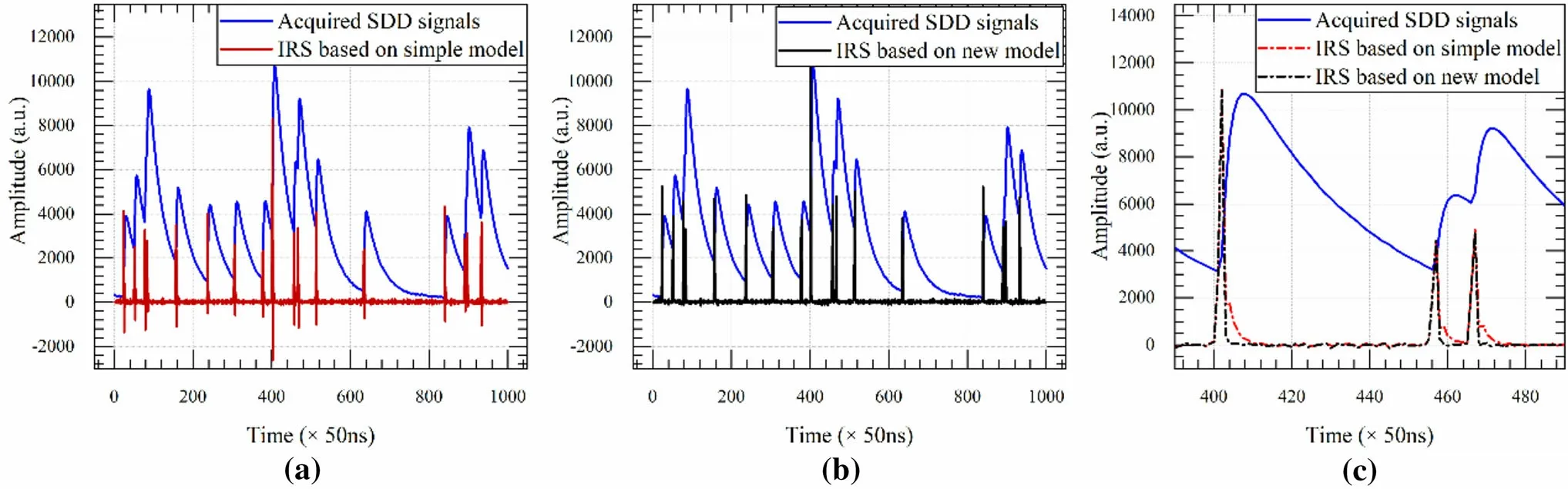
Fig. 6 (Color online) Unit IRS of acquired SDD signals. a Unit IRS of acquired SDD signals using the simple model. b Unit IRS of acquired SDD signals using the new model. c Unit IRS using the simple and new models

where d1=e-Ts/τ1,d2=e-Ts/τ2, and d3=e-Ts/τ3, with Tsbeing the sampling period.
A digital solution for the signals of the semiconductor detector system in the time domain is given by Eq. (27),which is obtained from Eq. (26) using the inverse Ztransform.Figure 6a also indicates that the undershoots of the pulses were large. Longer tails appeared after the pulse undershoots were eliminated by adjusting τ1,τ2,and τ3,as shown in Fig. 6c.The tailing phenomenon is attributed to the fact that the output-signal model described by Eq. (24) lacks the support of a physical model. The output signal expressed by Eq. (24) is the product of two signals with clear physical meaning. In a linear system, one signal cannot be directly multiplied by another signal.
As shown in Fig. 6b, the shaped pulses obtained using

If Vi(t) is defined by Eq. (8), the following digital solution can be obtained:the new model had no undershoot. Figure 6c presents the results for the two shaping methods. The unit impulse


The SDD signals obtained from the ADC were tested via Eqs. (27) and (28), that is, using the simple and new models, respectively, and the results are shown in Fig. 6.
As shown in Fig. 6a, the unit impulses of the SDD signals obtained using the simple model oscillated.obtained using the new model was narrower than that obtained using the simple model. Additionally, the unit impulse obtained using the new model had a shorter tail,while the noise remained at the same level. It can be concluded that the new model outperformed the simple model for processing overlapping signals.
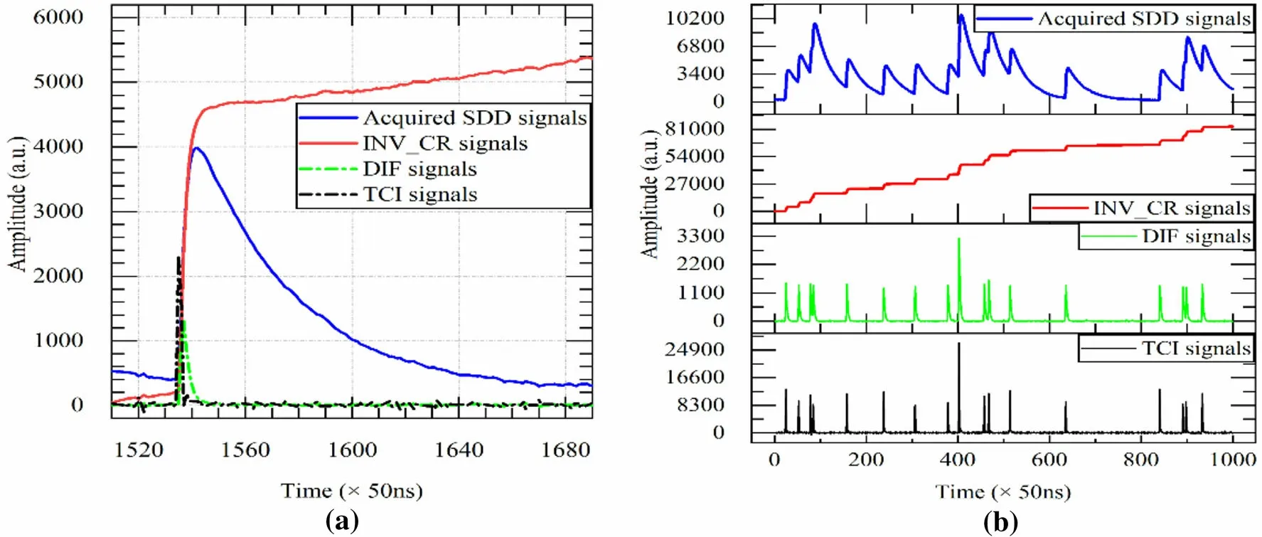
Fig. 7 (Color online) Test results for the MCD-IRS algorithm. a Test results for SDD signals. b Test results for SDD signals in high-counting rate environments
4.2.3 Quantitative comparison of output-signal models
Typically, the total full width at half maximum(FWHM) of the peaks is used to evaluate digital pulse shapers[23,24].However,there are several other methods for comparing unit IRS algorithms. In this study, two methods were employed:comparing the average peak base widths of the impulses and comparing the total areas of the impulses (a smaller total area corresponds to better unit IRS).
The SDD signals were tested using the two output-signal models. After adjustment of τ1, τ2, and τ3, the average amplitudes of the impulses obtained using the two models were essentially identical. The experimental results indicated that the total FWHMs and SNRs obtained using the two models had no significant differences.
However, the average peak base widths of the output shaped pulses obtained using the simple and new models were 6.017 × 50 ns and 3.793 × 50 ns, respectively; that is, the average peak base width was 36% smaller for the proposed model.Let the area of the impulse obtained using the new model be Anand the area of the impulse obtained using the simple model be As. Then, ∑Anand ∑Asrepresent the total areas of the impulses obtained using the two models. SDD signals with a length of 1000 were tested.The value of ∑Anwas 1.459 × 10⁵,the value of ∑Aswas 1.727 × 10⁵, and the value of ∑An/∑As was 84%.Additionally, for the simple model, small pseudo-peaks appeared on tails when the SDD signals overlapped significantly. Pseudo-peaks result can in pulse-counting rate errors. The results indicated that the new output-signal model described by Eq. (8) agreed better with the output SDD signals than the simple model proposed in [1].
4.3 Test and analysis of MCD-IRS algorithm
The acquired SDD signals were tested using the MCDIRS algorithm, and the results are shown in Fig. 7.
As shown in Fig. 7a, the width of the TCI output impulse was between 1 and 4 sampling points, the undershoots of the pulses were eliminated,and the shaped pulses had almost no tails.As indicated by Fig. 7b,the MCD-IRS algorithm stably processed SDD signals at high counting rates. In the experiments, 2 MB of acquired SDD signals were processed and shaped offline. The personal computer used in the experiments was equipped with an Intel CPU(i5-6200U) with 16 GB of random-access memory. The experimental results indicated that the average peak base widths of the output shaped pulses obtained using the traditional and new IRS algorithms were 3.793 × 50 and 3.363 × 50 ns, respectively; i.e., the average peak base width was 11% smaller for the proposed algorithm. The numbers of impulses obtained using the traditional and new algorithms were 29,970 and 30,004,respectively.The total elapsed time required for pulse shaping was 0.23 and 0.17 s for the traditional and new algorithms, respectively; i.e.,the total elapsed time required for pulse shaping was 26%shorter for the proposed algorithm. Offline processing results for the acquired SDD signals indicated that the digital solution described by Eq. (22) or (23) is consistent with the solution described by Eq. (28).
Equation (28), which was obtained using the Z-transform and inverse Z-transform, contains the recursive term Y[n-2]on the right-hand side.This term indicates that the result of each calculation depends on the previous calculation result. Owing to the noise and background in measured signals, there are errors in the calculations. These errors may accumulate and be transferred in calculation processes,affecting the output signals of the semiconductor detector system. Recursion increases the complexity of DPP systems. In DPP systems, a feedback network should be included owing to the recursive term. The feedback network affects DPP in high-speed and real-time systems.In the DPP system based on Eq. (28), signals can only be processed serially.The filter implemented using Eq. (28)is an infinite impulse response filter, which has parasitic oscillation in some cases.
In the implementation of the MCD-IRS algorithm,attention should be paid to multiple solutions to inverse systems. Multiple solutions may result in instability of the inverse system.For example, the MCD-IRS algorithm was unstable in the INV_CR system when processing signals whose baseline was not zero. However, when there was a direct series connection between the INV_CR and DIF systems,the MCD-IRS algorithm was stable.Figures 3 and 4 show a scheme for developing a stable algorithm based on the direct series connection between the INV_CR and DIF systems.
In tasks that use short word-length integers or fixedpoint data, FPGAs exhibit a high degree of parallelism.However, FPGAs cannot achieve the optimum performance in high-precision floating-point arithmetic operations [25, 26]. If the sampling rate of the digital system is sufficiently high, the sampling frequency can reach 100 MHz. In Eqs. (18) and (23), m, M, and K can be approximated as integers.Because the native data from the ADCs are integers, the algorithm can be simplified to integer arithmetic, which is suitable for implementation with FPGAs.
Pipelining is widely used in DPP systems to accelerate digital signal processing [27]. The main problem with conventional pipelining is that it is based on the propagation delay information [27]. The MCD-IRS algorithm is non-recursive; therefore, a pipeline scheme of the directform FIR filter can be implemented.
5 Conclusion
An output-signal model and a non-recursive IRS algorithm for the signals of semiconductor detector systems were proposed. The output-signal model was developed according to an analysis of the detector output signal-processing flow.It was tested and analyzed using the acquired SDD signals. The experimental results indicated that the average peak base width of the output shaped pulses obtained using the new model was reduced by 36% compared with that for the simple model proposed in [1]. The undershoots of the shaped pulses were eliminated, and the shaped pulses had almost no tails. Compared with the simple model, the new output-signal model agreed better with the output SDD signals and was more stable when shaping the SDD signals into unit impulses.
On the basis of the new model, an MCD-IRS algorithm is proposed. The new IRS algorithm was implemented using INV_RC, INV_CR, and DIF systems. Offline processing results for acquired SDD signals indicated that compared with the traditional IRS algorithm based on the Z-transform, the average peak base width of the output shaped pulses obtained using the new algorithm was reduced by 11%, and the total elapsed time required for pulse shaping was reduced by 26%. The proposed algorithm avoids recursive calculation.Pipeline schemes can be used to implement new algorithms.When the sampling rate of the digital system is sufficiently high, the algorithm can be simplified to integer arithmetic, which is suitable for implementation with FPGAs. The new non-recursive IRS algorithm is more suitable than the traditional algorithm for high-speed parallel processing of the acquired SDD signals. In high-counting rate environments, pulses overlap significantly, e.g., in the case of real-time online detection of industrial material compositions or rapid analysis of alloys. The MCD-IRS algorithm can be applied in these cases.
In the detection system for nuclear radiation, the amplifiers and the ADC affect the rising edge of the pulse.A cascade RC can be added to the proposed system to modify the rising edge of the semiconductor detector pulse.
Author contributions All authors contributed to the study conception and design. Material preparation, data collection and analysis were performed by Xue-Yuan Wang,Jian-Bin Zhou and Ming Wang.The first draft of the manuscript was written by Xue-Yuan Wang and all authors commented on previous versions of the manuscript. All authors read and approved the final manuscript.
杂志排行

Nuclear Science and Techniques的其它文章
- Development of a low-background neutron detector array
- Dication-accelerated anion transport inside micropores for the rapid decontamination of pertechnetate
- Iterative Bayesian Monte Carlo for nuclear data evaluation
- Sparing lung tissue with virtual block method in VMAT planning for locally advanced non-small cell lung cancer
- Decomposition of oil cleaning agents from nuclear power plants by supercritical water oxidation
- Nuclear mass based on the multi-task learning neural network method