Tin dioxide buffer layer-assisted efficiency and stability of widebandgap inverted perovskite solar cells
2022-05-12BingbingChenPengyangWangNingyuRenRenjieLiYingZhaoandXiaodanZhang
Bingbing Chen,Pengyang Wang,Ningyu Ren,Renjie LiYing Zhaoand Xiaodan Zhang†
1Institute of Photoelectronic Thin Film Devices and Technology,Renewable Energy Conversion and Storage Center,Solar Energy Conversion Center,Nankai University,Tianjin 300350,China
2Key Laboratory of Photoelectronic Thin Film Devices and Technology of Tianjin,Tianjin 300350,China
3Engineering Research Center of Thin Film Photoelectronic Technology of Ministry of Education,Tianjin 300350,China
4Collaborative Innovation Center of Chemical Science and Engineering (Tianjin),Tianjin 300072,China
5School of Physical Science and Technology,Inner Mongolia University,Key Laboratory of Semiconductor,Hohhot 010021,China
Abstract:Inverted perovskite solar cells (IPSCs) have attracted tremendous research interest in recent years due to their applications in perovskite/silicon tandem solar cells.However,further performance improvements and long-term stability issues are the main obstacles that deeply hinder the development of devices.Herein,we demonstrate a facile atomic layer deposition(ALD) processed tin dioxide (SnO2) as an additional buffer layer for efficient and stable wide-bandgap IPSCs.The additional buffer layer increases the shunt resistance and reduces the reverse current saturation density,resulting in the enhancement of efficiency from 19.23% to 21.13%.The target device with a bandgap of 1.63 eV obtains open-circuit voltage of 1.19 V,short circuit current density of 21.86 mA/cm2,and fill factor of 81.07%.More importantly,the compact and stable SnO2 film invests the IPSCs with superhydrophobicity,thus significantly enhancing the moisture resistance.Eventually,the target device can maintain 90% of its initial efficiency after 600 h storage in ambient conditions with relative humidity of 20%-40% without encapsulation.The ALD-processed SnO2 provides a promising way to boost the efficiency and stability of IPSCs,and a great potential for perovskite-based tandem solar cells in the near future.
Key words:atomic layer deposition;tin dioxide;additional buffer layer;efficiency and stability;inverted perovskite solar cells
1.Introduction
Recently,a record power conversion efficiency (PCE) of perovskite/silicon monolithic tandem solar cells has increased to 29.8%[1],which has broken the theoretical efficiency of a single junction silicon cells.With rapid progress in increasing PCE,perovskite/silicon tandem devices have become an inventive competitor in the photovoltaic performance race[2-4].Even though the single-junction perovskite device with N-I-P architecture presented power conversion efficiencies (PCEs)of 25.5%,in tandem devices the highest performance was obtained with inverted perovskite solar cells (IPSCs)[5-7].Therefore,surmounting the performance loss and instability issues of inverted perovskite devices are extremely important to accelerate the commercialization of perovskite/silicon tandem technology[8].
Up to now,the PCE of IPSCs has reached to 23.37% with a certificate efficiency of 22.75%[9],which was the highest value reported for IPVSCs.Compared with the normal N-I-P type PSCs,the large open-circuit voltage (VOC) deficit is considered as one of the main obstacles,particularly in wide bandgap IPSCs, which slows its performance development[10,11].Actually,plenty of research has been done for suppressing theVOCloss in IPSCs.These mainly include components regulation[12-14],crystallization control[15-17],bulk or surface defect passivation[11,18-23]and energy level alignment[24-27].Due to the easy solution coating process,the good physical and electronic contacts with the perovskite layer and the favorable passivation functionality,[6,6]-phenyl-C61-butyric acid methyl ester (PCBM) is one of the popular materials for the electron transport layer in IPSCs[28-30].However,the direct contact between PCBM and the top metal electrode will lead to serious non-radiative recombination,thus resulting in the failing collection of charge carriers to the cathode.Bathocuproine (BCP) is the most common material used in IPSCs to block hole transport and facilitate electron collection[9,18,28-32].Nevertheless,this insulating layer needs to be sufficiently thin to allow electron tunneling.In general,solution-processed perovskites have a rough surface,which makes the thickness of the insulator layer difficult to control.Therefore,a buffer layer that can achieve uniform coverage on the rough perovskite surface is the most pressing need for highly efficient IPSCs.
Besides the PCE,the main challenge for actual commercialization in PSCs lies instability[33-35].The electron transport layers (ETLs) play a more important role in IPSCs towards stable devices.Through rational design,the ETL can provide a self-encapsulating function.For instance,Youet al.employed solution-processed zinc oxide (ZnO) nanoparticles as electron transport layers,comparing with devices with organic charge transport layers,which showed~90% retention of its initial PCE after 60 days storage in ambient[36].Fanget al.designed a PCBM/cerium oxide (CeOx) nanocrystal bilayer structure with good long-term stability under ambient air storage[37].Tin dioxide (SnO2) with high electron mobility and a well band alignment with the perovskite absorption layer,which is a superior material in single-junction planar PSCs or highly efficient perovskite/silicon tandem solar cells[38-40].Zhuet al.exploited the solution-processed SnO2nanocrystals (NCs) to act as efficient ETLs in the IPSCs,a PCE of 18.8% with remarkable ambient stability was obtained[41].Raningaet al.used atmospheric pressure chemical vapor deposition (CVD) to achieve a pinhole-free and conformal SnO2layer,and thus protect the perovskite against mechanical and environmental destruction,resulting in a PCE of 19.4% in an IPSCs[42].
Here,SnO2using the atomic layer deposition (ALD) method was designed as an additional buffer layer on the BCP layer for improving efficiency and stability in wide bandgap IPSCs.Compared with previous methods,ultra-thin and compact SnO2could be obtained by ALD process.Moreover,vacuum conditions and suitable for large area fabrication also make it great potential for future commercialization.It was found that SnO2layer was homogeneously coated on the sample surface eliminating the possible leakage current and thus raising the shunt resistance (Rsh) and reducing the reverse current (J0).Finally,21.13% efficiency was obtained in the wide-bandgap (1.63 eV) inverted perovskite device with a SnO2additional buffer layer.Moreover,ALD growing SnO2layer with a great compactness which enhanced the moisture contact angle and improved stability of the perovskite device.
2.Experimental section
2.1.Device fabrication
ITO substrates were cleaned by detergent,DI water,acetone and isopropanol for 30 min,respectively.Then the substrates were treated by UV-ozone for 20 min.And then,PTAA(5 mg/mL in CB) solution was spin-coated onto the substrates at 5000 rpm for 30 s and annealed at 100 °C for 10 min in the glovebox with nitrogen condition.1.5 M PbI2:Pb-Br2(83 :17) precursor solution was spin-coated onto PTAA at the speed of 3000 rpm for 30 s and annealed at 70 °C for 1 min.And then,a mixture solution of organic salt (FAI :MABr :MACl=90 :6 :9) was spin-coated onto the film at a speed of 3500 rpm for 30 s followed by annealing at 150 °C for 20 min in ambient air (30%-40% humidity).The passivation layer GABr (3 mg/mL in IPA) was fabricated by spin-coating at 5000 rpm for 30 s followed by annealing at 100 °C for 5 min.Subsequently,PCBM solution (20 mg/mL in CB) was spincoated onto the perovskite film at a speed of 1500 rpm for 30 s.BCP solution (0.5 mg/mL in IPA) was spin-coated onto the PCBM film at a speed of 5000 rpm for 30 s.And then,the devices were moved into ALD devices to deposit SnO2film with different thicknesses.The deposition of the SnO2with the following processing sequence:0.5 s TDMASn pulse,15 s purge (20 sccm N2),0.1 s deionized water pulse,and 15 s purge (20 sccm N2) at 85 °C.Finally,150 nm of Cu top electrode were thermally evaporated under vacuum with a shadow mask.The area of the cells is 0.12 cm2,when measuring,a 0.0887 cm2mask was used to define the accurate aperture area for the cells.
2.2.Material and device characterizations
2.2.1.Materials
Lead bromide (PbBr2),chlorobenzene (CB),dimethylsulfoxide (DMSO),N,N-dimethylformamide (DMF) and isopropyl alcohol (IPA) were purchased from Sigma-Aldrich.Polybis (4-phenyl) (2,4,6-trimethyl-phenyl) amine (PTAA),[6,6]-Phenyl C61 butyric acid methyl ester (PCBM),bathocuproine (BCP),lead iodide (PbI2),bromide guanidine (GABr),formamidinium iodide (FAI),methylammonium bromide (MABr),and methylammonium chloride (MACl) were purchased from Xi’an Polymer Light Technology Corp.
2.2.2.Device characterizations
Scanning electron microscopy (SEM,FEI NanoSEM650)was used to characterize the morphology of the SnO2films and also the cross-sectional image of the fully device.The current density-voltage (J-V) characteristics of the devices were measured by Keithley 2400 Source meter under AM 1.5G illumination with Xenon-lamp based solar simulator (Enli.Tec.,Taiwan).The intensity of the light was calibrated with KG-5 filter Si photodiode.And the area of the solar cells was 0.08875 cm2.When measuring the device performance,a metal mask was used to reduce the influence of the scattered light.The forward scan (0-1.2 V,scan rate 20 mV/s,delay time 20 ms) and reverse scan (1.2-0 V,scan rate 20 mV/s,delay time 20 ms) were applied.External quantum efficiency(EQE) spectra were conducted by Enli Tec (Taiwan) measurement system in the wavelength from 300 to 900 nm with a scanning step of 10 nm.The photoluminescence (PL) and time-resolved photoluminescence (TRPL) spectroscopies were measured with a laser wavelength of 475 nm and power of 0.2 mW (Edinburgh FS5).The root mean square (RMS) roughness of different films was taken from atomic force microscopy (AFM) images measured with ARTCAM-130-SIINT (ARTRAY Co.Ltd.,Japan).
3.Results and discussion
Firstly,SnO2with different thickness as an additional buffer layer is designed.Fig.1(a) presents the illustration of the IPSCs devices with a structure of ITO/PTAA/Perovskite/PCBM/BCP/SnO2/Cu.The thickness of perovskite film is around 550 nm (Fig.S1).Current density-voltage (J-V) curves of the devices with SnO2films of different thicknesses (0,10,20,30,40 nm) are shown in Fig.1(b).The results demonstrate that the devices with SnO2layer obtain a higherVOCand fill factor (FF),short-circuit current density (JSC) is also slightly increased.The control device without SnO2layer achieves a PCE of 17.47%.When the thickness of SnO2film increased from 10-30 nm,the PCE is enhanced to 17.60,18.29 and 20.02,respectively.While the thickness of SnO2increased to 40 nm,the performance of IPSCs decreased to 19.82%,which may be due to the thick SnO2film introducing a high series resistance.The performance of IPSCs with different scanning directions are presented in Fig.S2 and Table S1.And the statistical diagrams of the device performances are shown in Fig.S3.After optimization,the device of 30 nm SnO2exhibited champion performance with aVOCof 1.19 V,JSCof 21.86 mA/cm2,FF of 81.07%,and the corresponding PCE of 21.13%.While,the control device only with a PCE of 19.23%.

Fig.1.(Color online) Device structure and performance with different SnO2 thickness.(a) The architecture of the device in this work.(b) J-V curves with different SnO2 thickness.(c,d) The champion devices J-V and EQE curves with 30 nm SnO2 buffer layer,respectively.
J-Vand external quantum efficiency (EQE) curves are presented in Figs.1(c) and 1(d),respectively.The integral current densities of the devices are 21.41 and 21.67 mA/cm2which are well matched with theJSCinJ-Vmeasurement.The bandgap of the perovskite can be determined by the tangent of the curve to the base line which is also presented.The ultraviolet-visible absorption of perovskite material and(αhν)2versus energy of perovskite film are shown in Fig.S4.It can be found that the bandgap of the perovskite is about 1.63 eV.Therefore,theVOCdeficit (Eg/q-VOC) is only of 440 mV.This value is a lowerVOCloss which compares to other wide bandgap IPSCs as present in Table S2.Moreover,device performance of different SnO2thicknesses with or without BCP are also investigated (Fig.S5).BCP is essential when a thinner SnO2is deposited.With increasing the thickness of SnO2,the role of BCP is gradually diminished.Devices with BCP and a suitable thicker SnO2buffer layer achieved a higher FF and PCE.
Time-resolved photoluminescence (TRPL) is employed to investigate the transport and recombination dynamics of photoinduced carriers in perovskite films without and with 30 nm SnO2buffer layer (Fig.2(a)).The biexponential function is applied to fit the TRPL decay curves (Eq.(1))[43]:

whereτ1andτ2are the lifetimes for the carrier transport and recombination,andA1andA2are the corresponding amplitudes.τ1is due to the carrier transport occurring in the surface of the perovskite film,whereasτ2could be attributed to the bulk and surface recombination.The devices without SnO2obtainedτ1=42.01 ns andτ2=146.43 ns,respectively.Whileτ1=37.65 ns andτ2=181.59 ns are given with SnO2.The decrease ofτ1indicates faster electron transfer from perovskite to ETL with the presence of SnO2.The increasedτ2indicates a slower recombination rate.The film with defferent thickness of SnO2film were also presented in Fig.S6,and the fitting value of the carrier transport and recombination lifetime were shown in Table S3.The results illustrate that perovskite film with SnO2additional layer achieves a faster carrier extraction and a lower carrier quenching between the active layer and the transport layer,which is a good agreement with the higher FF andVOC.Rshof the devices without or with 30 nm SnO2are also calculated (Fig.2(b)).The higherRshbenefits the enhancement of the FF,which further confirms the excellent function of the SnO2buffer layer.
Fig.2(c) shows the darkJ-Vcurves of the devices without and with a 30 nm SnO2buffer layer.According to the Schottky junction model,diode ideality factor (n) andJ0can be obtained by fitting the linearJ-Vcurve (exponential diode behavior region) as shown in Fig.2(d).The Eq.(2) shows in the following[44]:

Fig.2.(Color online) Device performance without the SnO2 buffer layer and with 30 nm SnO2 buffer layer.(a) TRPL curves of the devices.(b) Rsh of the devices.(c) J-V curves of the devices under dark condition.(d) Fitting curves for calculation the n and J0 from the dark J-V data.
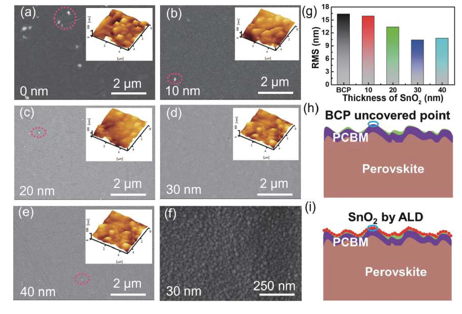
Fig.3.(Color online) Top view SEM of SnO2 layer with various thicknesses based on the structure of ITO/PTAA/Perovskite/PCBM.(a),(b),(c),(d)and (e) with thickness of SnO2 of 0,10,20,30 and 40 nm,respectively.(f) With a larger magnification to show a clearer morphology of SnO2 with the thickness of 30 nm.(g) RMS of the films with different thicknesses of SnO2.(h) The schematic diagram of the sample with a thinner BCP layer.(i) The schematic diagram of the sample with a BCP and SnO2 bilayer.

Fig.4.(Color online) (a,b) The water contact angle of the device without and with SnO2.(c-f) Normalized VOC,JSC,FF and PCE of perovskite devices without and with 30 nm SnO2 kept in the atmosphere (25 °C,20-40 RH%) without encapsulation for 600 h,respectively.
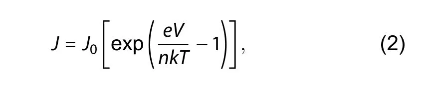
whereJis the current density value,Vis the applied voltage,Tis the absolute temperature,kis the Boltzmann constant,eis the electron charge.From the equation we can find thatnandJ0are close related with the slope and intercept of the linear fitting of ln(J0) versusV.The control device has a slope of 16.41,while the device with 30 nm SnO2film has a slope of 19.38.The larger the slope,the smaller then,which proved a better diode characteristic.The correspondingJ0values of 1.10 × 10⁻⁹and 1.22 × 10⁻⁸mA/cm2are obtained of the devices with and without SnO2film.The results clearly indicated that device with SnO2film has a lowerJ0,which means a smaller leakage current,resulting in a higherVOC.
A top-view scanning electron microscope (SEM) is primordially verified to show the surface morphology of the devices with or without SnO2(Fig.3).Figs.3(a)-3(e) were the SnO2film morphologies with the thickness of 0,10,20,30 and 40 nm on the structure of glass/ITO/PTAA/perovskite/PCBM/BCP,respectively.As expected,SnO2films with different thicknessness demonstrate different coverage,and the surface becomes increasingly compact as the thickness increases.SnO2with 10 nm obtains the poorest coverage while all of the devices with thickness over 20 nm show uniform and dense morphology,and the device with 30 nm SnO2has the best coverage.Fig.3(f) shows a clearer morphology of SnO2with the thickness of 30 nm,and it further illustrates that the compact SnO2layer can uniform coverage of the ETL layer,obstructing the immediate contact with the metal electrode.And the illustrations present the corresponding surface morphology of the films with different thicknesses of SnO2by an atomic force microscope (AFM).The root-mean-square (RMS)roughness of the films is shown in Fig.3(g),SnO2film deposited by ALD can effectively reduce surface roughness.The assumed schematic diagrams of the performance improvement are demonstrated in Figs.3(h) and 3(i).Perovskites with a rough surface,so the solution method BCP with a thinner thickness may not cover the PCBM completely.This supplies an opportunity of direct contact between PCBM and metal electrode,causing a non-radiative recombination center and reducing theRsh,and thus degrading the performance of the devices.Whereas,the ALD method SnO2can conformal growth on the uneven surface which completely prevents the current leakage.That more distinctly illustrates the reason of the increasedVOCand FF of the devices with SnO2additional buffer layers.
The water contact angles are presented in Figs.4(a) and 4(b).It is evidently shown that the film with a 30 nm SnO2layer has a larger contact angle which can better resistance to moisture and then stabilize the device.The devices without and with 30 nm SnO2are stored in a glove box with nitrogen (N2) condition (Fig.S7).Both of the devices show relatively high stability,the device performance with SnO2is basically keeping the same efficiency without decay after 600 h.Figs.4(c)-4(e) show the normalizedVOC,JSCand FF of the device with and without SnO2layer in the air atmosphere with relative humidity between 20%-40% without encapsulation,respectively.Fig.4(f) presents the normalized PCE of the devices with or without SnO2layer.It is clearly shown that the device with SnO2still maintains 90% of initial efficiency after 600 h.Nevertheless,the efficiency of the device without SnO2drops down to less than its 70%.We can find that the attenuation of the PCE is mainly due to the decrease of FF andVOC,while theJSCare barely changed.Fig.S8 presents the changes of series resistance (Rs) for the two devices,we supposed the increasedRsis the reason for the FF andVOClosses.
4.Conclusions
In summary,we have demonstrated that the ALD-processed SnO2as an additional buffer layer in IPSCs is a general approach to enhance the device’s performance and stability.The results show that this additional buffer layer can significantly increase theRshand reduce the leakage current,thus enhancing the FF andVOC.Meanwhile,the uniform SnO2film with good hydrophobicity to repelling moisture,which can retard the decomposition of perovskite film.The device with a SnO2buffer layer achieves over 90% of its initial efficiency after 600 h under an ambient condition with relative humidity of 20%-40%.Instead,the control device only exhibits 70%of its initial efficiency.This work provides a facile way of boosting the efficiency and stability of IPSCs,which also gives guidance for perovskite-based tandem solar cells for future commercialization.
Acknowledgements
B.B.Chen and P.Y.Wang contributed equally to this work.The authors gratefully acknowledge the supports from National Key Research and Development Program of China(Grant No.2018YFB1500103),the Overseas Expertise Introduction Project for Discipline Innovation of Higher Education of China (Grant No.B16027),Tianjin Science and Technology Project (Grant No.18ZXJMTG00220),and the Fundamental Research Funds for the Central Universities,Nankai University(Grant Nos.63191736,ZB19500204).Natural Science Foundation of Tianjin (No.20JCQNJC02070).China Postdoctoral Science Foundation (No.2020T130317).
Appendix A.Supplementary materials
Supplementary materials to this article can be found online at https://doi.org/10.1088/1674-4926/43/5/052201.
杂志排行
Journal of Semiconductors的其它文章
- Mechanism investigation of pre-existing void-induced multimodal electro-migration behavior
- Uniform,fast,and reliable CMOS compatible resistive switching memory
- Effect of charge trapping on electrical characteristics of silicon junctionless nanowire transistor
- Observation of resistive switching in a graphite/hexagonal boron nitride/graphite heterostructure memristor
- Double-balanced mixer based on monolayer graphene fieldeffect transistors
- Magnetic tuning in a novel half-metallic Ir2TeI2 monolayer