Effect of charge trapping on electrical characteristics of silicon junctionless nanowire transistor
2022-05-12YifanFuLiuhongMaZhiyongDuanandWeihuaHan
Yifan Fu,Liuhong Ma,,Zhiyong Duan,,and Weihua Han
1School of Physics and Microelectronics,Zhengzhou University,Zhengzhou 450001,China
2Engineering Research Center for Semiconductor Integrated Technology,Institute of Semiconductors,Chinese Academy of Sciences,Beijing 100083,China
3Center of Materials Science and Optoelectronics Engineering,University of Chinese Academy of Sciences,Beijing 100083,China
4Institute of Intelligence Sensing in Zhengzhou University,Zhengzhou 450001,China
Abstract:We investigated the effect of charge trapping on electrical characteristics of silicon junctionless nanowire transistors which are fabricated on heavily n-type doped silicon-on-insulator substrate.The obvious random telegraph noise and current hysteresis observed at the temperature of 10 K indicate the existence of acceptor-like traps.The position depth of the traps in the oxide from Si/SiO2 interface is 0.35 nm,calculated by utilizing the dependence of the capture and emission time on the gate voltage.Moreover,by constructing a three-dimensional model of tri-gate device structure in COMSOL Multiphysics simulation software,we achieved the trap density of 1.9 × 1012 cm-2 and the energy level position of traps at 0.18 eV below the intrinsic Fermi level.
Key words:junctionless transistor;charge trapping;random telegraph signals
1.Introduction
Rapid downscaling of metal-oxide-semiconductor fieldeffect transistors (MOSFETs) causes many adverse issues,such as short channel effects (SCEs) and carrier mobility degradation,which will seriously affect the performance of related devices.More seriously,as the size of MOSFETs continues to shrink to the nanometer scale,the fabrication process for the source/drain of the traditional inversion mode transistor is facing more challenges.In recent years,several novel materials have been proposed to keep up with the pace of Moore’s law,such as two-dimensional (2D) semiconductor materials[1,2].For traditional silicon materials,researchers try to improve device performance from the aspect of device structure.A silicon-based junctionless nanowire transistor (JNT) which can be considered as a gated resistor,has been proposed as a promising alternative to a new generation of transistors.The manufacturing process of JNT is relatively simple,with a constant doping concentration from source to drain and without any PN junctions.In addition,JNT is completely compatible with the CMOS manufacturing process[3-5].Compared with existing field-effect transistors (FETs),JNTs have more potential advantages due to junctionless characteristics.For example,the manufacturing complexity is reduced due to the low thermal budget and the requirement to eliminate junctions as well as reduce the SCEs[6,7].Consequently,JNT has the potential to become the sub-10 nm technology node and subsequent technical solution[8].
The key to the fabrication of JNTs is that the channel must be thin enough to ensure that the device is turned off at zero gate voltage.In addition,due to the excellent electrostatic controllability,the tri-gate structure is undoubtedly the best choice for JNT manufacture.Interface traps will be inevitably formed in the process of transistor fabrication,which will directly affect the electrical characteristics and reliability of devices[9-12].Owing to the large surface-to-bulk aspect ratio,the trapping and detrapping of the interface traps become crucial in JNT.Random telegraph signals (RTS) are fluctuations of the current between discrete levels.In nanoscale transistors,two-level fluctuations are generally attributed to the capture and emission of single carrier by traps in the gate oxide layer.Since the carriers in the JNTs are transported in bulk model,the noise signal caused by the surface roughness of the nanowire can be ignored.Hence,JNT is suitable to observe RTS introduced by the interface traps.Previous publications which describe the electrical characteristics for JNT mostly focus on ideal conditions[13-15].In fact,whether for long-channel or short-channel devices,the interface traps in the gate dielectric stack can affect the electrical properties of the devices,such as changing the threshold voltage,causing irregular current jump,and reducing the drive current.
In this paper,we fabricated tri-gate JNTs through experiments,and investigated the electrical properties of the fabricated devices at different temperatures.At low temperatures,we observed irregular current protrusions.This is a phenomenon caused by interface traps.We analyzed the influence of interface traps on the electrical characteristics of JNT by adding interface traps with different densities and different energy levels to a three-dimension (3D) model built by COMSOL Multiphysics simulation software[16].Besides,according to the trap density obtained by the experiment,combined with the simulation results,we get the energy level position of interface traps.This paper can provide guidance for the extraction of the spatial position and energy level position of interface defects in transistors.
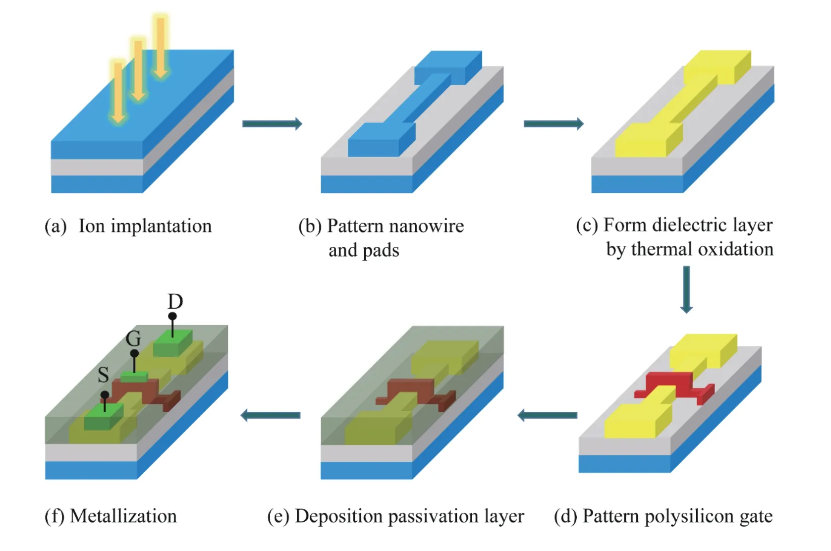
Fig.1.(Color online) Schematic diagrams of the fabrication process for JNTs.
2.Experimental methods
Fig.1 shows the schematic diagrams of the fabrication process of JNTs.The devices were fabricated on a silicon-on-insulator (SOI) substrate with the top silicon layer of 55 nm.The SOI wafer was uniformly and heavily doped by phosphorus ion implantation with a dose of 5 × 1013cm-2(Fig.1(a)).And then electron beam lithography (EBL) and inductively coupled plasma (ICP) etching were performed to define the active region and the channel fin (Fig.1(b)).It was followed by a sacrificial oxidation to eliminate the etching induced surface damage and then 22-nm-thick gate oxide was grown at 900 °C in dry oxygen for 1 h (Fig.1(c)).Then,a 150-nm-thick boron doped polysilicon gate was defined,wrapped around three sides of the silicon channel (Fig.1(d)).The poly-silicon was then doped by arsenic ion implantation at a dose of 1 ×1020cm-3after annealing at 1000 °C for 10 s.After depositing 200-nm-thick silicon dioxide as the protective layer,ohmic contact windows were opened (Fig.1(e)).Following 400-nm-thick aluminum was evaporated and lifted off as final metallization via conventional optical lithography (Fig.1(f)).The cross-section schematics and the scanning electron microscope (SEM) image of the tri-gate JNT are shown in Fig.2.The final cross section of the silicon core was estimated to be 30 nm in height (H) and 30 nm in width (W),respectively.The length of polysilicon gate (Lg) was 280 nm.For the low temperature electrical characterization,the devices were measured in a vacuum chamber,which can be cooled down to 10 K.The conventional operation of JNTs is to apply a positive gate voltage to create an electroneutral region in the channel region and allow electrons to flow.
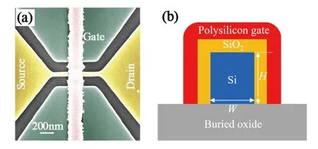
Fig.2.(Color online) (a) The color SEM image of devices with the gate length of 280 nm.(b) The cross-section schematics of the devices.
3.Results and discussion
Firstly,we tested the relevant electrical characteristics of the devices at room temperature.Fig.3(a) shows the transfer characteristic curves.The drain voltageVDSis set to be 0.1 to 4.1 V with the step of 1 V.As the gate voltageVGScontinues to increase,the drain currentIDSalso increases,gradually reaching a saturated state.The subthreshold swing (SS) and the threshold voltage (VTH) are 132 mV/dec and 0.26 V,respectively.The curves of drain currentIDSversusVGSshow that the fabricated JNT operates as a normally-off device with a low gate leakage current of several pA and the on/off current ratio larger than 1 × 10⁴.Besides,the output curves in Fig.3(b)demonstrate excellent gate control ability in our devices.
The temperature-dependent electrical properties of JNT were carried out by Lakershore-340 temperature controller under vacuum environment.Fig.4(a) shows the output characteristics of JNT measured at the temperature of 10 K.Obvious current jumps are observed at some special values ofVGSsuch as 2.20 V.Besides,the current jumps increase with the increase of the absolute value of the bias,indicating the existence of active traps[17].For the analysis of current hysteresis,a single staircase voltage ramp was used.The gate voltageVGSwas varied by 0.02 V steps and the duration of each step was 0.1 s,andVDSwas set to be 0.2 V.In the forward sweep,the forward bias was increased from 0 to 3.5 V.In the backward sweep,the sweep started at 3.5 V,and was gradually decreased to 0 V.The measured results are shown in Fig.4(b).The curves clearly show hysteretic nature.The current hysteresis behavior is larger than that measured during the reverse sweep.This is because the charging and discharging process are slower than the sweep rate,leading to identical currents in both sweep directions due to the fact that the traps cannot remain in the same initial state[18].
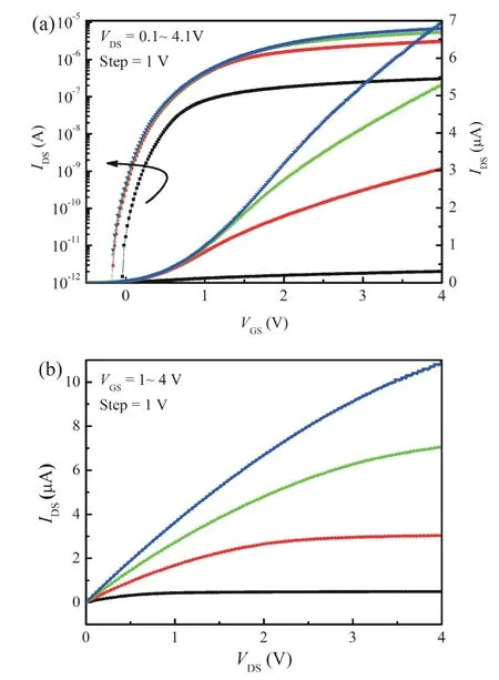
Fig.3.(Color online) Measured drain current characteristics at room temperature,showing (a) drain current versus gate voltage for drain voltages of 0.1 to 4.1 V with step of 1 V,and (b) drain current versus drain voltage for gate voltages from 1 to 4 V with step of 1 V.
Fig.5(a) shows the transfer characteristic curve of this device at a low temperature of 10 K.The drain voltage is set to be 2-10 mV with the step of 2 mV.Obvious current jumps are observed around the gate bias of roughly 2.2 V,at which voltage,the trap level and the silicon channel Fermi level move close to each other so that hopping and tunneling happen.The trap is found to be an acceptor type center[19].Typical time domain current levels are shown in Fig.5(b).The average time at the highest current level,so-called the capture timeτc,decreases asVGSincreases.It is ascribed to the fact that the electron concentration in channel increases with increasingVGS.The average time at the lowest current level,can be considered as the emission timeτe.The accurate vertical trap depthxTcan be extracted by the following expression[20]
wheretoxis the oxide thickness,kis Boltzmann constant andqis the elementary charge.Through linear fitting ofVGSdependence of ln(τc/τe) as shown in Fig.6,the accurate vertical trap depth obtained by Eq.(1) is 0.35 nm.Compared to the oxide thickness of 22 nm,these traps can be considered as interface traps.
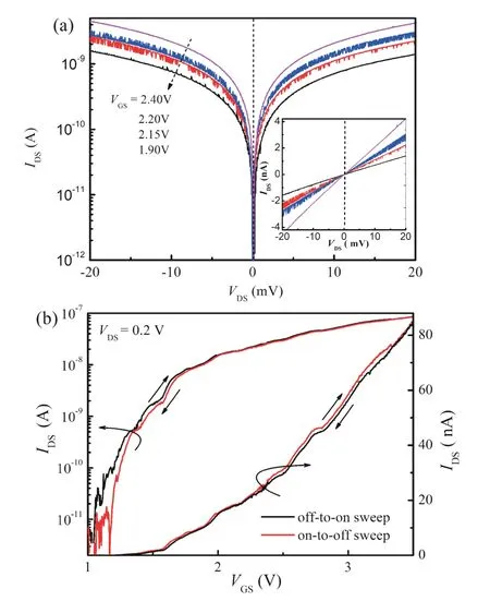
Fig.4.(Color online) (a) IDS-VDS output characteristics of JNT device at T=10 K.(b) The transfer characteristics of the JNT with VGS sweep from 0 to 3.5 V and back.
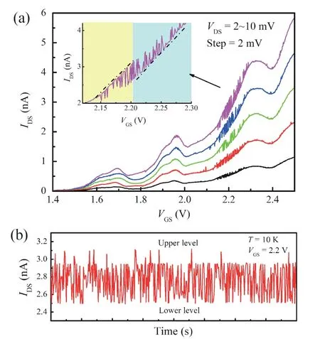
Fig.5.(Color online) (a) IDS-VGS curves for VDS values ranging from 2 to 10 mV in steps of 2 mV.The detail image in the upper left corner is an enlarged detail.(b) Time domain current levels versus time trace at VGS=2.2 V and VDS=10 mV.
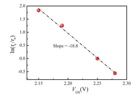
Fig.6.(Color online) ln(τc/τe) and its linear fitting.The slope is proportional to xT,the position of the traps in the oxide.
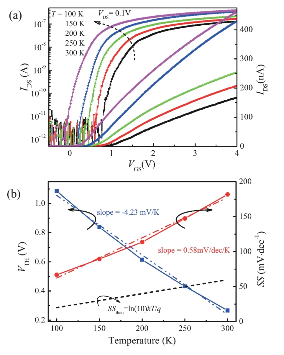
Fig.7.(Color online) (a) Transfer characteristics at the temperatures of 100 to 300 K with the step of 50 K.(b) Measured VTH and SS at VDS=0.1 V versus temperature.The black dashed line represents the theoretical value of subthreshold swing SStheo.
In Fig.7(a),the measuredIDSas a function of theVGSwith the device biased at a drain voltage ofVDS=0.1 V is presented for different temperatures.It can be noted that the drain current decreases with temperature.The threshold voltageVTHand subthreshold swing SS are presented as a function of the temperatures in Fig.7(b).The slope ofVTHvaried with the temperatures is an approach to -4.23 mV/K and the slope of SS is 0.58 mV/dec/K.It should be noted that the SS variation with temperatures of our JNT device is larger than that of the theoretical value.We attribute this phenomenon to the influence of interface traps.The subthreshold swing SS depending on the trap densityNtrapis described by[21]
whereCoxis the gate oxide capacitance per unit area (estimated to be 1.56 × 10⁻⁷F/cm2).The presence of interface traps will deteriorate the subthreshold characteristics.The interface trap density obtained from Eq.(2) is approximately to be 1.9 × 1012cm-2.
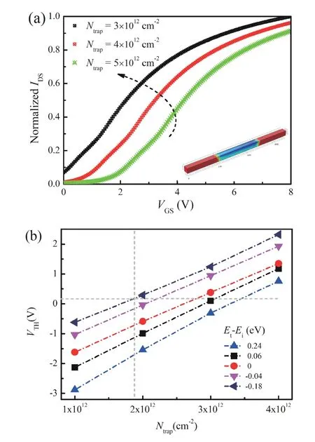
Fig.8.(Color online) (a) Simulated IDS-VGS curves for different trap densities with the trap level equals to the intrinsic Fermi level.(b)Threshold voltage as a function of trap densities with different trap levels.
To further investigate the influence of interface traps on JNT electrical characteristics,we construct a 3D tri-gate JNT structure in COMSOL Multiphysics simulation software with the Semiconductor Module.The parameters of the simulation device are consistent with the experimental device.The gate with a 22-nm-thick oxide layer and surface traps is modeled using the thin insulator gate boundary condition around the perimeter of the channel.The drain and source boundaries are ideal ohmic contacts,and the voltages are set to ground and 0.1 V,respectively.The gate voltage is swept from 0 to 8 V for different surface trap densities.The simulated device structure is shown in the insert of Fig.8(a).Here,LsandLdare the distances of the source and the drain from the channel region,respectively.Those two parameters are set to 200 nm.At first,the influence of trap density on the transfer characteristic is investigated.The simulated curves are shown in Fig.8(a).The transfer curves are positively shifted with increasing interface trap density.Besides,the influence of the trap levels is also investigated in Fig.8(b).Here the energy difference between the trap energy levelEtand the intrinsic Fermi levelEiis set as -0.18,-0.04,0,0.06 and 0.24 eV,respectively.For the same trap density,the threshold voltage will shift positively as the trap level moves away from the conduction band.Therefore,combining the experimental data with the simulation results,we obtain that the position of trap level is 0.18 eV below the intrinsic Fermi level,and the trap density is 1.9 ×1012cm-2.
4.Conclusion
In summary,we fabricated junctionless tri-gate nanowire transistors on the SOI substrate.We analyzed the electrical properties of the manufactured devices at different temperatures (10-300 K).Obvious RTS were observed at low temperature of 10 K.This phenomenon indicates that there are acceptor-like trap states in the devices.Through linear fitting of gate voltage dependence of ln(τc/τe),the accurate vertical trap depth of 0.35 nm is obtained.Thus,the acceptor-like traps can be considered as interface traps.Besides,from the slope of the subthreshold swing versus temperature,we estimate the interface trap density to be 1.9 × 1012cm-2.In addition,we use COMSOL Multiphysics simulation software to build a 3D model for the device.In the model,traps with different densities and different energy levels are added to the interface between the conductive channel and the gate dielectric layer.According to the simulation results of threshold voltage,we estimate that the energy level of the interface traps is located at 0.18 eV below the intrinsic Fermi level.The results provide a theoretical guidance for analyzing the effects of interface traps on the junctionless transistors.
Acknowledgements
This work is supported by the National Natural Science Foundation of China (Grant Nos.613760966,1327813,61404126 and 11947115),the Natural Science Foundation of Henan Province under (Grant No.202300410444),and Foreign Experts Program of Ministry of Science and Technology in China (Grant No.G2021026027L).
杂志排行

Journal of Semiconductors的其它文章
- Mechanism investigation of pre-existing void-induced multimodal electro-migration behavior
- Uniform,fast,and reliable CMOS compatible resistive switching memory
- Tin dioxide buffer layer-assisted efficiency and stability of widebandgap inverted perovskite solar cells
- Observation of resistive switching in a graphite/hexagonal boron nitride/graphite heterostructure memristor
- Double-balanced mixer based on monolayer graphene fieldeffect transistors
- Magnetic tuning in a novel half-metallic Ir2TeI2 monolayer