Double-balanced mixer based on monolayer graphene fieldeffect transistors
2022-05-12MinWuWeidaHongGuanyuLiuJiejunZhangZiaoTianandMiaoZhang
Min Wu,Weida Hong,Guanyu Liu,Jiejun Zhang,Ziao Tian,,and Miao Zhang,
1School of Microelectronics,University of Science and Technology of China,Hefei 230022,China
2Shanghai Institute of Microsystem and Information Technology,Chinese Academy of Sciences,Shanghai 200050,China
Abstract:Graphene field-effect transistors (GFET) have attracted much attention in the radio frequency (RF) and microwave fields because of its extremely high carrier mobility.In this paper,a GFET with a gate length of 5 μm is fabricated through the van der Walls (vdW) transfer process,and then the existing large-signal GFET model is described,and the model is implemented in Verilog-A for analysis in RF and microwave circuits.Next a double-balanced mixer based on four GFETs is designed and analyzed in advanced design system (ADS) tools.Finally,the simulation results show that with the input of 300 and 280 MHz,the IIP3 of the mixed signal is 24.5 dBm.
Key words:GFET;mixer;RF;simulation;IIP3
1.Introduction
Since the discovery of monolayer graphene[1],graphene has become an attractive candidate to replace or supplement traditional semiconductors due to its excellent electrical and mechanical properties,as well as high compatibility with standard processes.Compared with semiconductors,only one atomic layer thickness,ultra-high carrier mobility[2-4]and higher saturation velocity[5]make it possible to produce graphene field-effect transistors (GFETs) with higher cut-off frequencies[6].Bipolar transmission is a main feature of GFETs,that is,the conductivity of GFETs can be controlled by holes or electrons.It results in a ‘V’-shaped transfer characteristic (Ids-Vgs)[1].Due to its unique ambipolar transport properties and extremely high mobility,graphene provides a wide range of applications for radio frequency and microwave fields.
Because of these excellent characteristics,graphene was used in practice,such as frequency multipliers[7,8],voltage amplifiers[9],ring oscillators[10],and mixers[11].Graphene is even being studied in fields related to RF switches[12]and memory[13].The study of graphene mixers is particularly concerned.Mixers are essential for almost all telecommunications and radar equipment,and limit the intermodulation performance of the receiver front end.Schottky barrier diodes and active FETs are the most commonly used mixer elements in microwave systems,but the linearity of these mixers is very low due to the strong nonlinearity of these devices.In contrast,the linear output characteristics of graphene makes it particularly suitable for such circuit applications.Although unsaturation is detrimental to traditional amplifier circuits,it is an advantage of resistive mixers now.Palacioset al.prepared a graphene resistive mixer for the first time using the characteristics of graphene bipolar transport.Conversion loss was 30-40 dB and IIP3 was 13.8 dBm at 10 MHz[14].In Ref.[15],the first graphene integrated circuit work was to realize a resistive mixer.Moonet al.also used the structure to prepare a graphene mixer,and showed the IIP3 of 22 dBm at a LO power of -3.5 dBm[16].
This paper explores the potential of graphene mixers.In order to further improve the linearity of the mixers,a graphene double-balanced mixer with four GFETs with crosscoupling structure is designed.The circuit structure is based on a proposed GFET large-signal model in ADS for circuit simulation[17].And it achieves IIP3 of 24.5 dBm with a LO signal of-2 dBm at 280 MHz.The main performance characteristics of the double-balanced GFET mixer are compared with CMOS technologies and the reported GFET mixer.
2.Monolayer graphene field-effect transistor
2.1.GFET fabrication
In this work,the transistor was fabricated on a high-resistance silicon (>10 kΩ·cm) substrate with 1μm thick silicon oxide.Monolayer graphene is grown on Ge substrate by chemical vapor deposition (CVD) method[18],and germanium-based graphene is used as a smooth substrate.Then 50 nm Au was evaporated by UV lithography and electron beam as source and drain,next 3 nm Al was evaporated by electron beam,after that 30 nm Al2O3was grown by ALD as the gate dielectric layer,and then 50 nm Au was evaporated by electron beam as the top gate electrode.Finally,the PVA solution was dripped,and after the PVA was dried,the metal (source and drain)/oxide layer (gate dielectric layer)/metal (gate) sandwich layer was transferred to the SiO2/Si (>10 kΩ·cm) with graphene channel.A GFET is formed on the substrate,and the graphene channel forms a vdW contact with the contact electrode.This transfer process reduces the damage of photolithography to the graphene channel and the contact resistance,which can have better device performance[19-21].
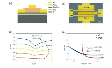
Fig.1.(Color online) (a) Schematic of top-gated Al2O3/monolayer graphene FET.(b) Photograph of a dual-finger gate 5-μm-length and 70-μmwide graphene FET.(c) Measured data for the Ids-Vgs characteristic curves at Vds=0.1 to 1 V.(d) Current gain,|H21|,and unilateral gain,U,with deembedding at Vds=0.8 V.
Fig.1(a) shows a 3D schematic diagram of GFETs on SiO2/Si.Fig.1(b) is an optical microscope image of GFETs with a dual-finger gate and ground-signal-ground (GSG) structure for the RF test.The gate lengthLgis 5μm and gate widthWis 70μm.Fig.1(c) presents the transfer characteristic curve (Ids-Vgs) of the GFET atVds=0.1 to 1 V and the Dirac point was observed to be located at aroundVdirac=-0.2 V.We adopt standard de-embedding method for avoiding the influence of parasitic capacitance and inductance of the GSG pad[22].And we prepared the open circuit and short circuit structure of the same device size to ensure reliable de-embedding results.In Fig.1(d),we show the current gain |H21| and the unilateral gain |U| of the GFET withLg=5μm andW=70μm atVds=0.8 V.The highest (intrinsic) maximum oscillation frequencyfMAXof~603 MHz and the highest (intrinsic)cutoff frequencyfTof~368 MHz are found.
2.2.A large-signal model of monolayer GFET
During circuit design,accurate GFET models are required to predict device and circuit performance.The small signal model cannot describe the nonlinear effects of the device to meet the simulation requirements of nonlinear circuits such as mixers and oscillators.However,the large signal model can give the complete characteristics of the device.Several models of GFET were developed recently[23-27].This article uses a monolayer GFET large-signal behavior model developed by Jan Stakeet al.and based on the drift-diffusion equation[17].
In this model,the graphene quantum capacitance will be ignored when the thickness of the gate dielectric layer is greater than 10 nm.And we also ignore the quantum capacitance of graphene.The model can be implemented by Verilog-A language in ADS environment.
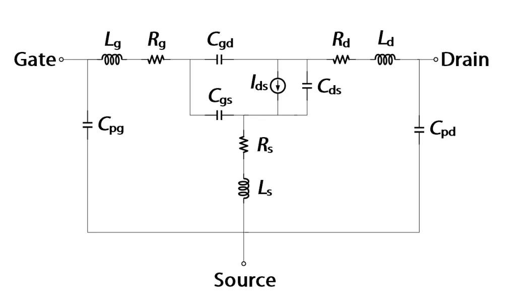
Fig.2.Large-signal model of a GFET.Cpd,Cpg,Lg,Ld and Ls are pad parasitic capacitance values and inductances,Rg is the gate resistance,and Rs and Rd are the source and drain resistances including contact and access resistances.
The schematic of a monolayer GFET large-signal model is presented in Fig.2.The current in the channel can be expressed as:
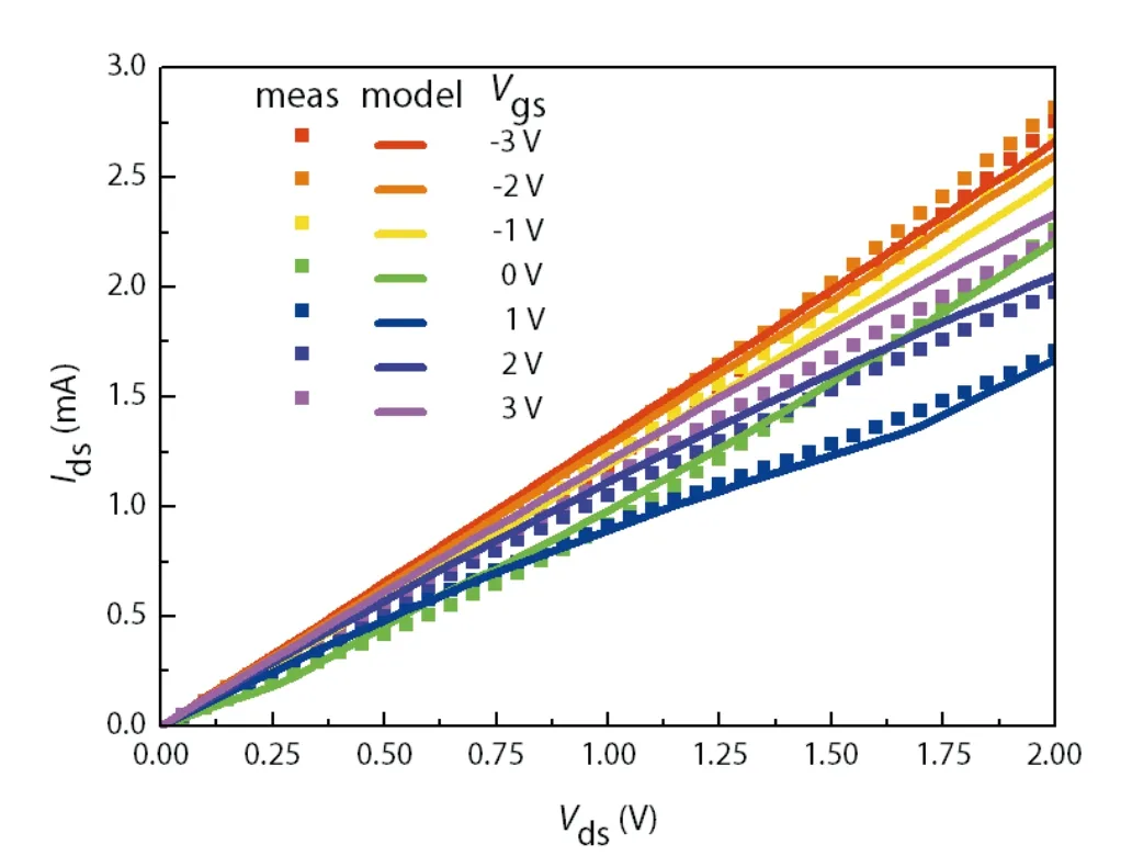
Fig.3.(Color online) Model versus measured data for the Ids-Vds characteristic curves at Vgs=-3 to 3 V.
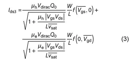
withVgs< 0,Vgd> 0.
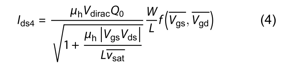
withVgs< 0,Vgd< 0.
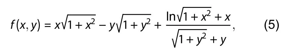
Among them,the following function is defined as:
Resistance between the source and drain can be expressed as:
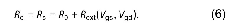
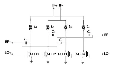
Fig.4.Schematic of the GFET double-balanced mixer.
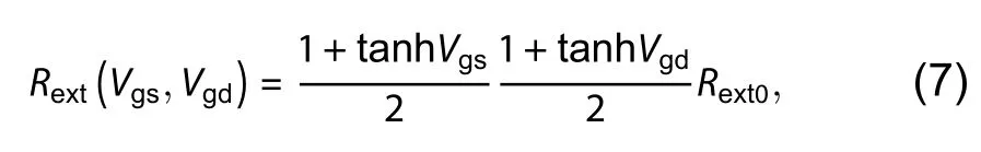
whereR0is the contact resistance andRext0is an extra resistance when the majority carriers are electron.
Intrinsic capacitors were extracted byS-parameters biased at Dirac voltage (Vgs=Vdirac,gm=0).By de-embedding theS-parameters, we can get:Cgd=-Y12/jω,Cgs=(Y11+Y12)/jω,Cds=Im(Y22+Y12)/ω.The model parameter extraction method in Fig.2 is the same as the method described in Ref.[17],and the parameters were extracted as shown in Table 1.The behavior model is implemented by Verilog-A and is compatible with ADS.As shown in Fig.3,the solid lines are the measured output characteristic curve (Ids-Vds)of the GFET,showing excellent linearity.The dotted lines are the output characteristic curves of the GFET DC simulation.It can be seen that the model is consistent with the measurement results.The large-signal model will be applied to subsequent mixer circuit design in section 3.

Table 1. GFET large-signal model parameters.
3.GFET double-balanced mixer
3.1.GFET mixer circuit design
Compared with a single GFET mixer,a graphene doublebalanced mixer can have better linearity and can suppress the feedthrough of RF and LO signals[28].The circuit diagram of the GFET double-balanced mixer in this article is shown in Fig.4.It consists of four GFETs with cross-coupling structure and four LC components,in which the inductance is 25 nH and the capacitance is 25 pF.The LC component has a filtering function,and LO,RF and IF are all differential signals.The four GFETs (withLg=5μm,W=70μm) operate atVgs=-0.6 V andVds=0.8 V.And the mixer is simulated in ADS.Due to the linear characteristics of the GFET,the mixer is expected to have a high linear output.
3.2.Simulation of the GFET double-balanced mixer
Fig.5 shows the RF performance of the GFET doublebalanced mixer.Fig.5(a) presents the simulated conversion loss (CL) versus LO power with a minimum CL of 23 dB at 300 MHz.Fig.5(b) is IF power versus RF power withfLO=280 MHz (4 dBm) andfRF=300 MHz.The dots in the figure are simulated data,and the line is the linear fitting,indicating that the 1 dB compression point is 6.5 dBm.Fig.5(c) reveals the simulated two-tone spectra of the mixer.The thirdorder intermodulation product (IM3) is 85 dBm lower than IF with RF power of -20 dBm.According to IIP3=RFin+(IF -IM3)/2,IIP3 is calculated as 22.5 dBm.The fundamental and the third-order term in the output signal versus RF power are shown in Fig.5(d).After linear fitting and expansion,the IIP3 is displayed as 24.5 dBm.In Table 2,the main performance of the mixer reported in this article is compared with the recently reported GFET mixer and CMOS mixer.It can be seen from the table that the designed mixer in this paper has more excellent linearity.
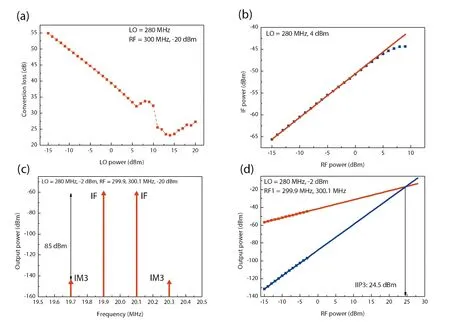
Fig.5.(Color online) RF performance of the double-balanced mixer.(a) Simulation result of conversion gain.(b) Simulation result of -1 dB compress point.(c) Simulated two-tone spectrum of the mixer.(d) Simulation result of IIP3.
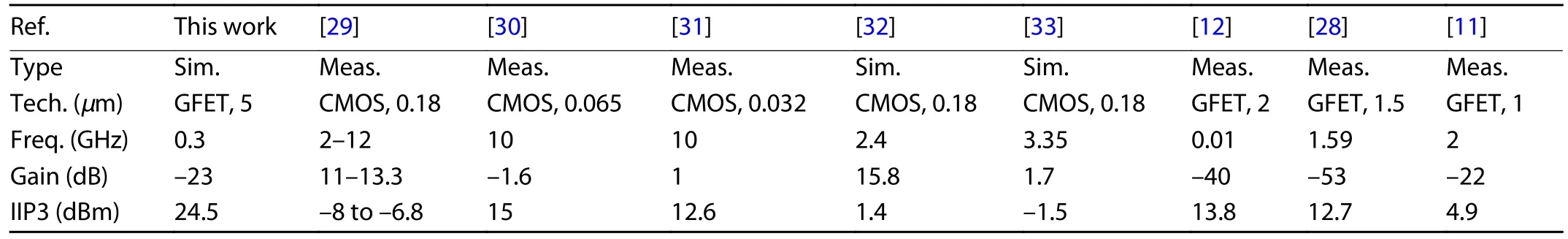
Table 2. Comparison between performance parameters of GFET and CMOS mixer.
4.Conclusion
In this work,we prepared a monolayer GFET by transfer process and assessed the DC and RF characterization.And we performed large-signal modeling on the GFET,which is written in Verilog-A and connected in ADS.A double-balanced mixer is designed based on the GFET and it provides a IIP3 of 24.5 dBm at 300 MHz.Compared with traditional CMOS mixers and GFET mixers that have been reported,it has better linearity.In addition,the operating frequency of the mixer is only limited by thefTof the GFET,and the gate length of the GFET can be reduced to broaden the operating frequency[34].
Acknowledgements
The authors thank National Natural Science Foundation of China (Grant Nos. 51925208, 61974157, 61851401,62122082),Key Research Project of Frontier Science,Chinese Academy of Sciences (QYZDB-SSW-JSC021),National Science and Technology Major Project (2016ZX02301003),Science and Technology Innovation Action Plan of Shanghai Science and Technology Committee (20501130700),Strategic Priority Research Program (B) of the Chinese Academy of Sciences(XDB30030000) and Science and Technology Commission of Shanghai Municipality (19JC1415500).
杂志排行
Journal of Semiconductors的其它文章
- Mechanism investigation of pre-existing void-induced multimodal electro-migration behavior
- Uniform,fast,and reliable CMOS compatible resistive switching memory
- Effect of charge trapping on electrical characteristics of silicon junctionless nanowire transistor
- Tin dioxide buffer layer-assisted efficiency and stability of widebandgap inverted perovskite solar cells
- Observation of resistive switching in a graphite/hexagonal boron nitride/graphite heterostructure memristor
- Magnetic tuning in a novel half-metallic Ir2TeI2 monolayer