Competitive effect between roughness and mask pattern on charging phenomena during plasma etching
2022-04-15PengZHANG张鹏andRuvarasheDAMBIRE
Peng ZHANG (张鹏) and Ruvarashe F DAMBIRE
1 School of Electronic Information Engineering,Yangtze Normal University,Chongqing 408100,People’s Republic of China
2 School of Chemistry and Chemical Engineering, Yangtze Normal University, Chongqing 408100,People’s Republic of China
Abstract In the plasma etching process, the edge roughness and mask pattern usually play a significant role in the deformation of holes under the influence of the charging effect.The competitive effect between these two factors has been investigated,focusing on the surface charging in a hexagonal array, with various values of roughness parameters (amplitude (A) and wavelength (W)) and distances between holes (L).A series of classical particle dynamic simulations of surface charging, surface etching and profile evolution were used to investigate the effect of roughness and pattern on charging.This study showed that various roughness and patterns(represented by different values of L) can significantly influence surface distributions of the electric-field (Efield)and the etching rates on the mask surface.The simulations also showed that(1)the shape of the pattern array influences the mask hole profile during the etching process,i.e.a hexagonal array pattern tends to deform the profile of a circular mask hole into a hexagonal hole;(2)pattern roughness is aggravated during the etching process.These factors were found to be significant only at a small feature pitch and may be ignored at a large feature pitch.Possible mechanisms of these results during the etching process are discussed.This work sheds light on the ways to maintain pattern integrity and further improve the quality of the pattern transfer onto the substrate.
Keywords: plasma etching, pattern, roughness
1.Introduction
Plasma etching is often used in manufacturing integrate devices,such as,microelectronic mechanical systems[1]and ultralarge-scale integration devices [2, 3].With the continuous shrinking of device sizes,increasing requirements are being put on the plasma etching technique [2, 4, 5].For instance, precisely controlling the etched-profile,dependence of aspect ratio(microscopic uniformity), and the critical dimension (CD),accompanying that of selectivity, etching rate as well as damage.The high-quality pattern transfer process is the decisive factor in the etching of high aspect ratio features.In the fabrication of microelectronic devices, surface roughness exerts a general side effect and can be crucial for a variety of fields and related applications [6, 7].For example, serious waveguide scattering loss might be caused by the roughness in the polymeric waveguide components[8].In other aspects,the wetting properties of etched surfaces are affected by the roughness,which has been demonstrated by several literatures[9–12].Roughness might also affect the electrokinetic efficiency [13] as well as the pressure drop during the polymeric microfluid fabrication[14].Moreover,the issue of roughness in nanometer- or even atomic-scale on the surface or profile of etched features has become more and more important.This is ascribed to the fact that the CD or the thickness of the layer being etched currently is comparable with the nanoscale roughness.
Additionally, many experiments have already shown that the mask pattern tends to deform the shape of mask holes to that of the pattern.For instance, one of our previous papers indicates that the hexagonal pattern deformed the profile of mask holes as hexagon[15].In the work of Negishi et al[16],it can be clearly seen that quadrilateral mask pattern made the profile of mask holes as quadrangle after etching in figure 6.Until now, there is already a great deal of research indicating that both the roughness generated by the nanoscale damage in the etching process and the pattern effect are caused by the charging effect [15–21].For example, Negishi’s work [16]verified that the pattern deformation mode changed from‘roughness’ to ‘wiggling’ depending upon the pattern depth.However, these two factors contribute quite different features of profile evolution.The roughness tends to amplify the nonuniformity of the profile, while the pattern effect focuses on changing the shape of the profile.Therefore, we can raise at least two issues about these two factors.Specifically,(1)which one dominates as the distance between holes changes? (2)Whether there is an appropriate distance where the combinational effect by these two can make the minimal damage to the mask profile? It is predictable that, investigating these two issues will be quite valuable for better design of mask pattern and reduction of the mask pattern damage, which is beneficial to improve the quality of the pattern transfer.Unfortunately,there are no studies aimed to answer these issues yet.
The focus of this work is on discussions of the surface charging on seven rough mask holes in a hexagonal array,with various values of roughness parameters and distances between holes, with the emphasis being given on the surface distributions of the E-field and the etching rate,and the profile evolution of holes with time.
2.Simulation method and case study
The modeling framework consists of three modules as shown in figure 1: surface charging, surface etching and the profile evolution modules, which is spirited by the framework used by Memos et al [22–24], Rangelow’s group [25] and Kushner’s group [26].Briefly speaking, the energy and angular distributions of ions and electrons as well as the initial mask surface profiles are taken as the inputs.These variables are then updated by the spatial E-field calculated in the surface charging module and by the profile evolution module,respectively.The surface etching module is adopted to calculate the local etching rate.More details of the description of this framework as well as the proof of its validity can be found in some of our previous papers[27,28].The details of the calculation of the etching rate covered in this paper have been presented in the [27, 28].
The case study here is the etching of seven rough mask holes aligned in a hexagonal array with equal distance between each two adjacent holes (shown in figure 2(a)).The mask material is the 193 nm photoresist (ArF resist), rather than the generally-used amorphous carbon layer (ACL).The reason for such choice is, on one hand, due to the fact of the poor etching resistance of the ArF, which is very suitable for the consideration of roughness.On the other hand, the purpose of this work is just only to investigate the charging effect on the surface of the mask, thus it is actually completely unimportant if ArF is replaced by ACL.For the same reason,the selection of the substrate material has nothing to do with the final results of this study,even if we must address that the situation might be different when a dielectric substrate and a thin mask are used.Moreover, as stated in one of our previously published papers [15], because of the purpose of studying charging effects on the top of mask surfae, only the 2D mask plane (not the 3D geometric structure, shown in figure 2(b) (right)) that particles impinge on was investigated on by this work.However,as a statement,the model itself is a 3D feature.The trajectory of ions and electrons is traced according to Newton’s equation in a 3D coordination.Simply put,once a particle falls on a square grid in the 2D plane,the value of the charge of this grid is subtracted (for an electron)or added by one(for an ion).Then,the later coming particles are subjected to the E-field force calculated by this charge value.In summary, in this paper, a 3D feature model is simulated and only 2D result is investigated and shown.Certainly, it must be admitted that charging and charge distribution varies with mask depth.The profile evolution also is impacted by those charges inside the hole.Unfortunately,this cannot be simulated by our current program.It is believed that the influence from the depth on the profile evolution of the mask surface should have potential research value.This topic will be examined in future research.In addition,other effects that can cause or reduce roughening also(such as by-product re-deposition which can further influence charging effect)are ignored.Figure 2(b) (left) illustrates the process of how each rough hole was generated.Based on the bucking theory which has been successfully used to describe the roughness by pioneers [23, 29], the roughness can be parameterized by the wavelength (W) and the dominant amplitude (A).The W is defined as the node interval as figure 2(b) (left) shows.The values of W and A covered in this study are selected based on the experimental measurements in [29].First of all, a perfect round consisting of a series of nodes was used as the input(each two adjacent nodes were connected by a straight line).The radius of this round, R was taken as 0.05 μm.Second,each node was given a random advancement which satisfies a Gaussian distribution:
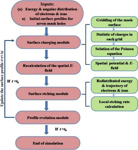
Figure 1.The flowchart of the modeling framework.
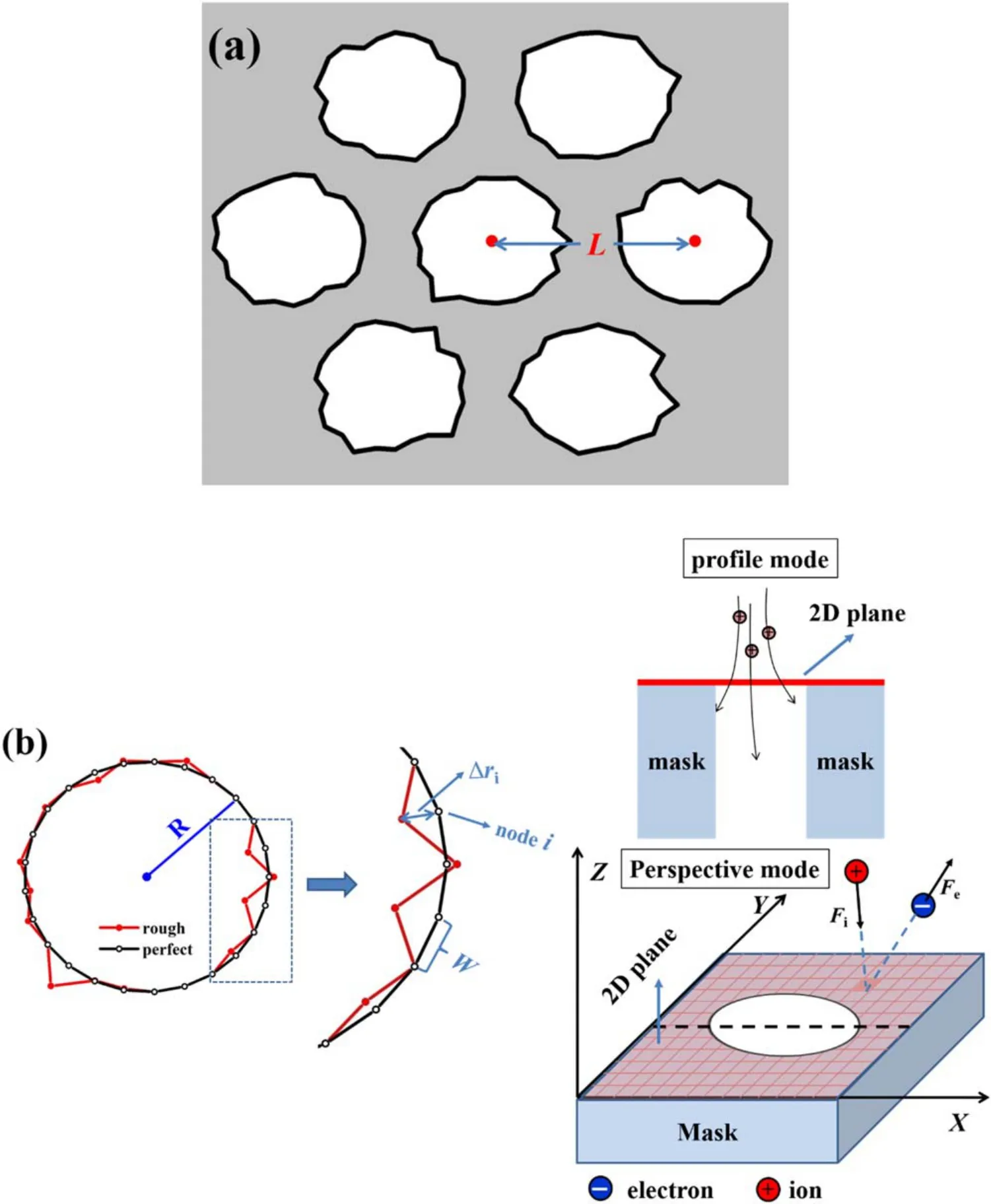
Figure 2.A schematic diagram of (a) seven rough mask holes aligned in a hexagonal array with equal distance between each two adjacent holes(top-down view).L indicates the distance between two adjacent holes,which is the distance between their centers.(b)Left:one rough mask hole constructed by nodes.The size of this rough hole is defined by the radius of its initial-perfectly round as the black line marked.A zoomed region indicates the definitions of Δri and W.The radii of all holes were set as 0.05 μm.Right:illustrating the 2D mask plane for the simulation where particles impinge on.In perspective mode: a schematic diagram illustrating the motion of one electron and ion being subjected to the E-field on the 2D surface of a mask according to Newton’s equation and Cartesian coordinates.Fi and Fe are the forces taken by the falling ion and electron, respectively.The profile mode was extracted along the dashed line through the center of the hole in perspective mode.
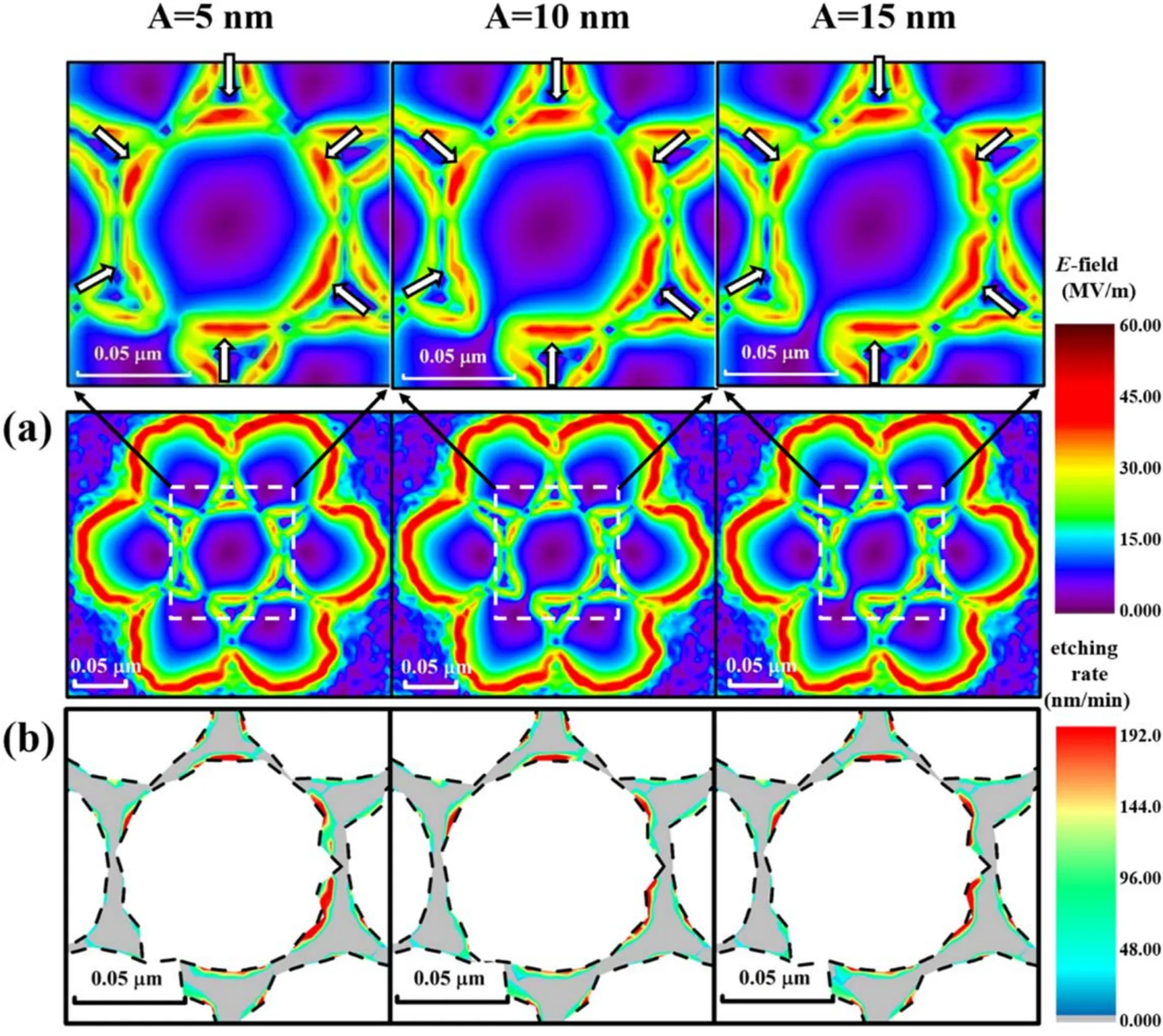
Figure 3.Simulated distributions of E-field strength and etching rate on the top of the mask surface with various initial values of A at etching time,t=0 s;(a)E-field strength,(b)etching rate.The values of W and L are 12 nm and 0.1 μm,respectively.The enlarged E-field strength around the central hole is above (a).The initial profiles of all holes are indicated by dash lines in (b).

Here,Δriis the advancement of ith node and σ=A/3.Another 0 to 1 distributed random number was used to determine the direction ofΔri(inward or outward).The center of each rough hole is defined as the same as that of its initialperfectly round.The distance of each two adjacent holes(indicated by L in figure 2(a)) is defined as the distance between their centers.When the mask profile is under the etching, each node shifts toward the material inner along the normal vector direction at the next time instant, according to the etching rate at that moment in this node calculated in surface etching module.The types of particles used in simulation are electron and CF4ion.The average energies for electron and ion were set as 3 and 90 eV, respectively.The ion flux is taken as 1.9×10²⁰m-2s-1.More detailed descriptions can be found in [27].
3.Results and discussion
In fact, only the E-field strength in the horizontal component above the mask surface is responsible for the trajectory deflection of the ion flux, which is the root reason for the deformation of the mask pattern.Therefore,it is significant to examine the relation between the horizontal E-field(called Efield in below for short) with distance and roughness first.Figure 3 shows a case of holes being so closely spaced(L is 0.1 μm).In figure 3(a),a series of simulated distributions of E-field on the top of the mask surface with various values of A at time, t=0 s is shown.Here, the moment that all electrons have reached the surface was selected as the timing point.Thus,the E-field at t=0 s was generated by electrons.It can be seen that, first of all, all the outer six holes (except for the central one)present the strongest E-field at their edges.This is due to the boundary effect of the calculation region.As a fact of the matter,the mask size is about several hundred square millimeters with a large number of holes.In consideration of the periodicity of the mask pattern, the surrounding of each hole can be viewed as identical.Therefore,the central hole can approximately represent all holes in a real mask, which is due to the small boundary effect and local periodicity on it.Obviously, the central hole displays a quite different E-field distribution compared to others.A local enlarged zone above figure 3(a) shows a non-uniform with hexagonal E-field distribution around the edge of the central hole (indicated by white arrows).This is caused by the hexagonal aligned mask pattern [15].However, there is no obvious difference among the E-field in various values of A(for initial profiles).This is because the influence from the pattern is dominant compared to the A in the case of the small value of L.Of course,in practice, both the values of A and L as well as the E-field distribution are time-dependent.Thus,it is necessary to further investigate the etching rate distribution and the subsequent profile evolution.Figure 3(b) poses a series of simulated distributions of etching rate on the top surface of the central hole with various values of A.Apparently,the etching rate presents a similar distribution to that of the E-field.This is attributed to the fact that, at the initial moment(t=0 s),the places with the strongest E-field attract more ions to bombard.Actually, there is still some tiny differences between them.This is because the trajectory of the ions is not only affected by the surface E-field (even it is the strongest), but also by E-field at different heights.In fact, as the detailed analysis for figure 3 in one of our published literature [30] shows, the E-fields in various heights present quite different strengths and distribution shapes.Moreover,the strength decreases with height.Thus ions will not bombard the mask surface strictly according to the E-field clinging to the surface.As a statement, holes will merge as a whole one, rather than overlap after over-ething.The current model cannot simulate their merging process yet.When they‘touch’each other, the simulation will end.
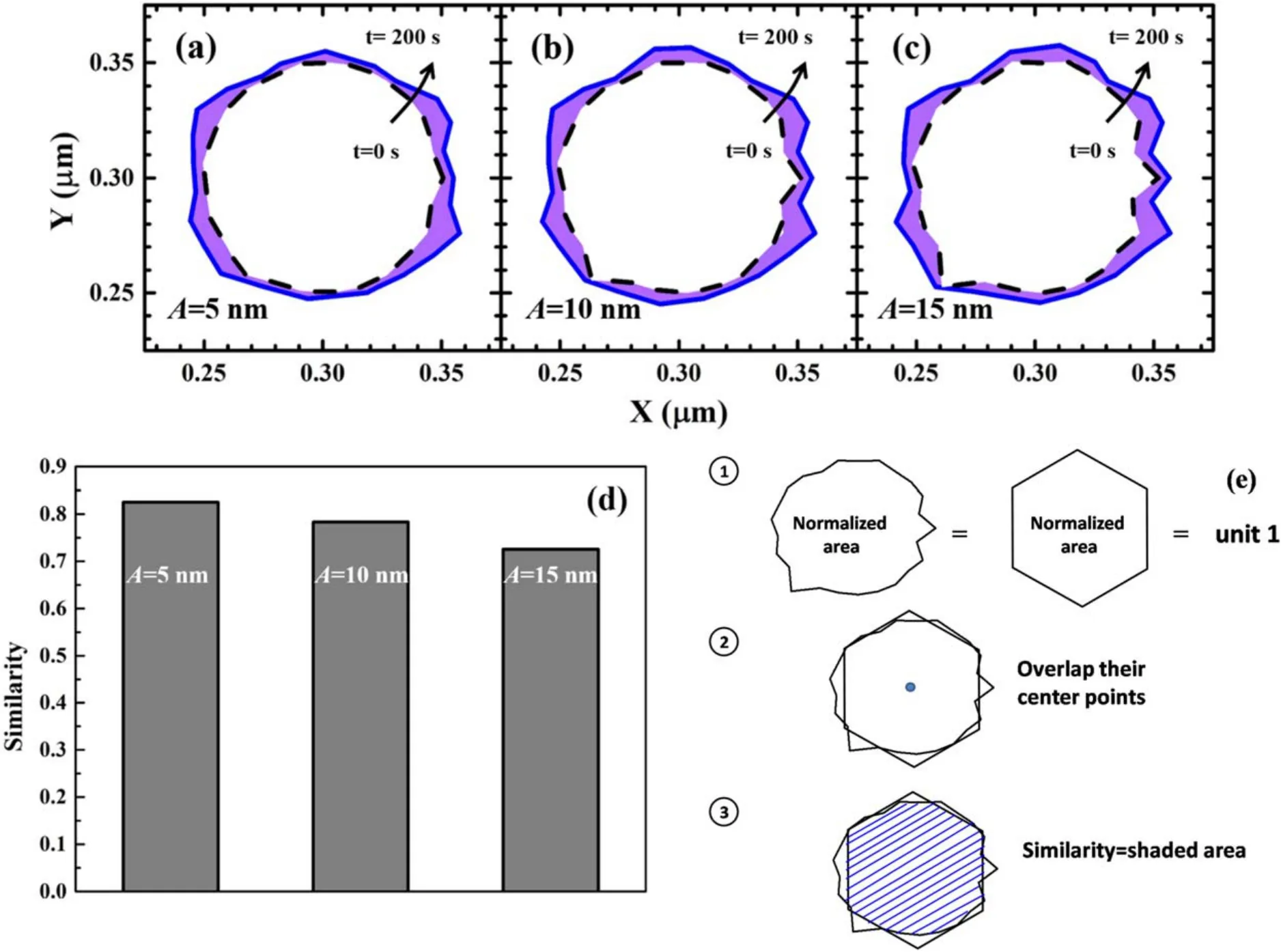
Figure 4.A series of simulated profile evolutions of the central hole with various initial values of A.(a) A=5 nm, (b) A=10 nm and (c)A=15 nm.Other geometric parameters are the same as those in figure 3.The simulated evolution time step-length is 100 ms.The values of W and L are 12 nm and 0.1 μm, respectively.(d) The similarity of the etched-profile (at t=200 s) to a regular hexagon, (e) the schematic diagram illustrating the method to calculate the similarity.
Figures 4(a)–(c) show a series of simulated profile evolutions of the central hole with various initial values of A.It can be seen that all etched-profiles (at t=200 s) present the hexagonal shape, but with slightly increased roughness compared to the initial ones.In order to quantitatively analyze the competitive effect between pattern and roughness,figure 4(d)further gives the similarity of the etched-profile(at t=200 s) to a regular hexagon.The calculation of the similarity is as follows(figure 4(e)illustrates the method):(1)normalize the areas of the profile and a regular hexagon as unit 1; (2) make their center points be overlapped; (3) obtain the overlapped area of which the value is the similarity.In figure 4(d), the similarity gradually descends with A, indicating the roughness indeed affects the profile evolution but is not dramatic at the near distance.
Figure 5 shows a case of the large value of L.On the contrary, it can be clearly observed that the central hole does not exhibit the hexagonal distribution of E-field no matter what the A is (shown in figure 5(a)).This is attributed to the weak/strong influence of the pattern/roughness at the long distance.In addition, these zoomed areas indicate that the larger the A is, the much more non-uniform E-field is presented.The corresponding etching rates which herald quite different profile evolutions are shown in figure 5(b).Figures 6(a)–(c)further illustrate a series of simulated profile evolutions with various values of A.
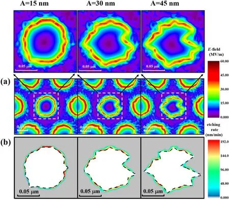
Figure 5.Simulated distributions of E-field strength and etching rate on the top of the mask surface with various initial values of A at etching time,t=0 s;(a)E-field strength,(b)etching rate.The values of W and L are 12 nm and 0.175 μm,respectively.The enlarged E-field strength around the central hole is above (a).The initial profiles of all holes are indicated by dash lines in (b).
Apparently, the etched-profile at the time of 200 s gradually goes further away from the hexagon as the value of A increases.But compared to the case of short distance(figures 4(a)–(c)), the extent of the changing of profiles is obviously larger after the same etching time.This is because the number of electrons falling on the surface in the long distance was larger than that in the short distance,resulting in higher E-field strength to attract ions bombardment (see figure 7).In addition, figures 6(a)–(c) show a fact that the mask profile is elongated along the X direction more compared to the Y direction resulting in an oval shape.This observation is attributed to the fact that the surroundings of the central hole in X and Y directions are different.In the X direction, there are two edges of the other two adjacent holes directly toward to the central hole, which is quite different from the situation in the Y direction.Figure 6(d) shows the similarities of the etched-profile (at t=200 s) and initial profile(at t=0 s)to a regular hexagon.Similarly,it displays the same tendency for the etched-profile as figure 4(d)shows except for the values, which are lower than those in figure 4(d).In addition,the similarities of the initial profile in all cases of A are a little bit larger than those of etched-profile.This reflects that the impact of A to the profile is dominant in the case of the large value of L.This is because, although the distance between holes actually is getting small with etching,which further promotes the influence of pattern to the profile, just the roughness of each hole becomes worse simultaneously.It exerts a stronger influence on the mask deformation than the pattern.To sum up to this point, a concise conclusion can be given that the influences of pattern and A to the deformation of the mask profile are dominant in the dense and sparse arrays, respectively.
Thus, logically, there should be a middle distance which makes the influence of these two factors reach a draw.Figure 7 shows the simulated distributions of E-field strength on the top of the mask surface with the same value of A(15 nm) in the case of various values of L.The distribution shape of the E-field around the central hole illustrates a transition from the non-uniform (hexagonal) to the uniform(not exactly due to roughness).The corresponding profile evolutions (figures 8(a)–(c)) show that the shape of the etched-profile in the case of middle distance (L=0.135 μm)is closer to an ideal shape(round)rather than a hexagon or an arbitrary shape.This is due to the competitive effect between those two factors.In figure 8(d), the lowest similarity to hexagon(grey)and the highest one to round(red)in the case of L of 0.135 μm verify that conclusion above.Here, the calculation of similarity to round is exactly the same as that described in figure 4(d),just with the hexagon being replaced by the circle.
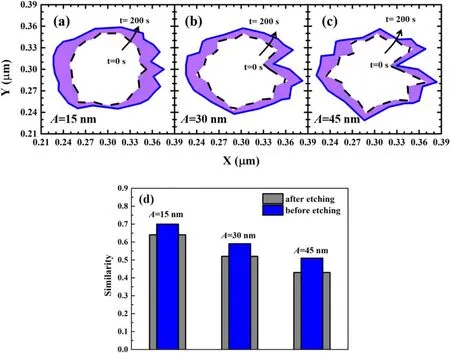
Figure 6.A series of simulated profile evolutions of the central hole with various initial values of A.(a)A=15 nm;(b)A=30 nm and(c)A=45 nm.Other geometric parameters are the same as those in figure 5.The simulated evolution time step-length is 100 ms.The values of W and L are 12 nm and 0.175 μm, respectively.(d) The similarities of the etched-profile (at t=200 s) and initial profile (at t=0 s) to a regular hexagon.
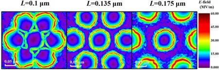
Figure 7.Simulated distributions of E-field strength on the top of the mask surface with various values of L at etching time, t = 0 s.The values of W and A are 12 nm and 15 nm, respectively.

Figure 8.A series of simulated profile evolutions of the central hole with various values of L.(a) L=0.1 μm, (b) L=0.135 μm and (c)L=0.175 μm.Other geometric parameters are the same as those in figure 7.The simulated evolution time step-length is 100 ms.(d) The similarities of the etched-profile (at t=200 s) to a regular hexagon (grey) and a regular round (red) at three different values of L.
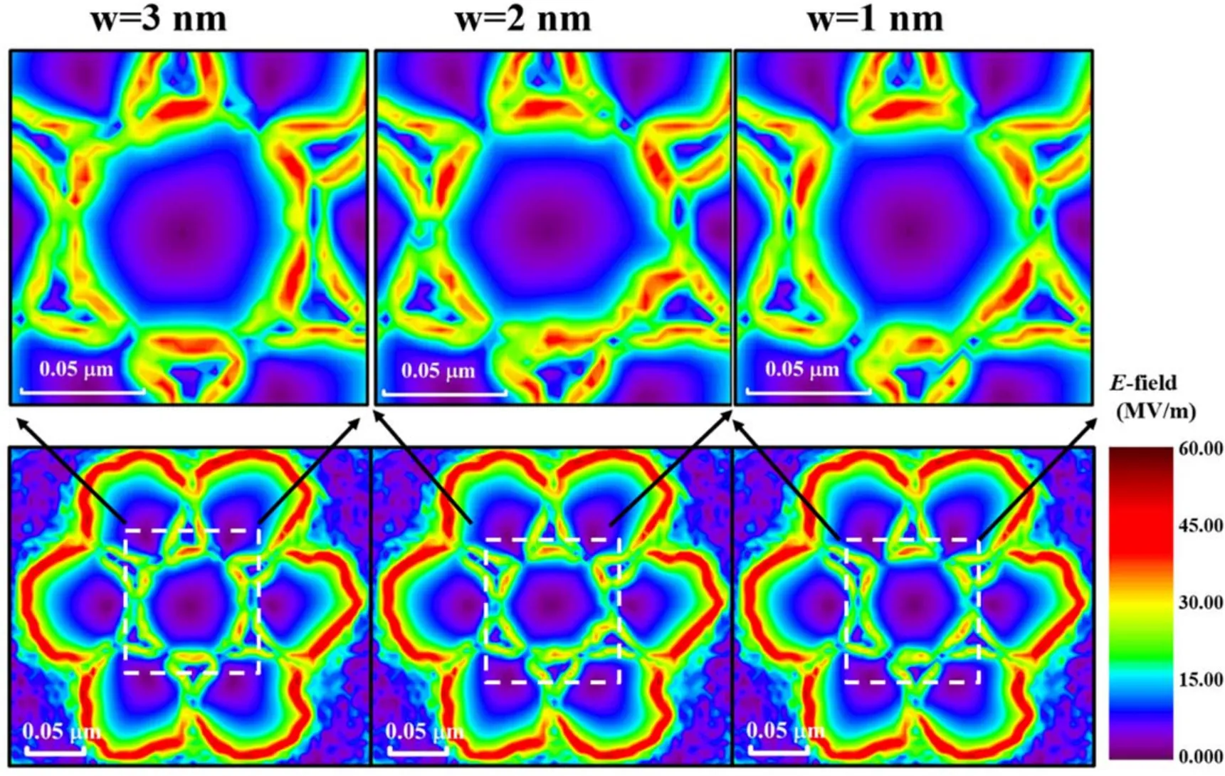
Figure 9.Simulated distributions of E-field strength on the top of the mask surface with various values of W at etching time, t=0 s.The values of A and L are 15 nm and 0.1 μm, respectively.The enlarged E-field strength around the central hole is above (a).

Figure 10.Simulated distributions of E-field strength on the top of the mask surface with various values of W at etching time, t=0 s.The values of A and L are 15 nm and 0.175 μm, respectively.The enlarged E-field strength around the central hole is above (a).
As stated above, another roughness parameter is the W(node interval shown in figure 2(b)).Therefore,it is beneficial to briefly explore what will happen if the value of W varies.Based on the results about parameter A, it can be found that the essential physical quantity is the E-field.Thus,here, only the E-field distribution is under discussion for W.Figure 9 shows a series of simulated distributions of E-field on the top of the mask surface with various values of W at time,t=0 s.Similarly, there is also no obvious difference among the Efield in various values of W,indicating that the influence from the pattern is dominant compared to the W in the case of the small value of L.Figure 10 displays the case of the larger value of L.It can be seen that the central hole also does not exhibit the hexagonal distribution of E-field no matter what the W is.This is attributed to the same reason explained in figure 5 that weak/strong influence of the pattern/roughness at the long distance.In addition, these zoomed areas also indicate the larger the W is, the much more non-uniform Efield is presented.Certainly, this work has not involved the mechanism of the ion reflection yet.Because this mechanism might interfere with the redistribution of the E-field as well as the profile evolution, it is better if the framework can implement the reflection effect.Our future work will further investigate the potential competitive effects between pattern,roughness with ion reflection.In addition, as the E-field is generated by the local imbalance of electrons and ions, the pattern effect should be affected by the energy and angular distributions of launched electrons.In our previously published work[28], it is concluded that by narrowing the shape of the electron angular distribution, the mask pattern damage can be strongly reduced.In that case, due to only an isolated mask hole being studied,it is reasonable to speculate that the mask pattern effect must be also affected by the electron angular distribution.Future work will also carry out this issue.
4.Conclusions
On the basis of a reliable modeling framework, the competitive effect between pattern and roughness has been investigated focusing on the surface charging on seven rough mask holes in a hexagonal array, with various values of roughness parameters (A and W).It was found that the influences of pattern and roughness to the deformation of the mask profile are dominant in the dense and sparse arrays, respectively.Specifically speaking,in a certain distance,the pattern impact tends to deform the profile of mask holes as a hexagon (the more rear the distance is,the more obvious will be),however,the roughness tends to break the pattern impact (the further the distance is,the stronger the intervention will be).There is an appropriate distance where the influence of pattern and roughness negate each other.In that situation, it can be seen that the evolution of the profile might get to an ideal shape(round) by the similarity analysis.The current work provides a crucial method to optimize the etching technique.
Acknowledgments
This work was supported by Youth Project of Science and Technology Research Program of Chongqing Education Commission of China (No.KJQN201901407), the start-up research funding of Yangtze Normal University, China (No.2017KYQD113), 2017 Youth Research Talent Supporting Program, China (No.2017QNRC18).
猜你喜欢
杂志排行

Plasma Science and Technology的其它文章
- Design and preliminary test of a 105/140 GHz dual-frequency MW-level gyrotron
- Reliability improvement of gas discharge tube by suppressing the formation of shortcircuit pathways
- A novel flexible plasma array for large-area uniform treatment of an irregular surface
- Pulsed high-current discharge in water:adiabatic model of expanding plasma channel and acoustic wave
- Comparison of double layer in argon helicon plasma and magnetized DC discharge plasma
- Physical design of a new set of high poloidal mode number coils in the EAST tokamak