Effect of layer sliding on the interfacial electronic properties of intercalated silicene/indium selenide van der Waals heterostructure
2022-03-23MasoodYousafYounisAhmedJbaraJunaidIqbalKhanMurtazaandSaeed
Masood Yousaf, M W Younis, Ahmed S Jbara, M Junaid Iqbal Khan,G Murtaza and M A Saeed
1 Department of Physics,Division of Science and Technology,University of Education,Lahore,54770,Pakistan
2 Department of Chemistry,University of Management and Technology,C-II,Johar Town,Lahore,54770,Pakistan
3 Mathematics Department, College of Education for Pure Science, Al-Muthanna University, Samawah,66001, Iraq
4 Laboratory of Theoretical and Experimental Physics, Department of Physics, Bahauddin Zakariya University, Multan, 60800, Pakistan
5 Materials Modelling Lab, Department of Physics, Islamia College Peshawar, KP, Pakistan
6 Department of Mathematics & Natural Sciences, Prince Mohammad Bin Fahd University, P.O.Box 1664, Alkhobar 31952, Saudi Arabia
Abstract Methods capable of tuning the properties of van der Waals(vdW)layered materials in a controlled and reversible manner are highly desirable.Interfacial electronic properties of two-dimensional vdW heterostructure consisting of silicene and indium selenide(InSe)have been calculated using density functional theory-based computational code.Furthermore, in order to vary the aforementioned properties,silicene is slid over a InSe layer in the presence of Li intercalation.On intercalation of the heterostructure, the buckling parameter associated with the corrugation of silicene decreases from 0.44 Å to 0.36 Å, whereas the InSe structure remains unaffected.Potential energy scans reveal a significant increase in the sliding energy barrier for the case of intercalated heterostructure as compared with the unintercalated heterostructure.The sliding of the silicene encounters the maximum energy barrier of 0.14 eV.Anisotropic analysis shows the noteworthy differences between calculated in-plane and out-of-plane part of dielectric function.A variation of the planar average charge density difference,dipole charge transfer and dipole moment have been discussed to elucidate the usability spectrum of the heterostructure.The employed approach based on intercalation and layer sliding can be effectively utilized for obtaining next-generation multifunctional devices.
Keywords: vdW heterostructure, intercalation, tuning of properties, layer sliding, interfacial electronic properties
1.Introduction
Since the isolation of graphene [1], numerous investigations[2–4] have focused on strategies for overcoming the intrinsic downside, which is the zero band gap of graphene.The aforementioned drawback along with its confined properties limits potential applications of graphene-based nanoelectronics, regardless of it having excellent charge carrier mobility [5].Recently, researchers have focused on heterostructures(HS)based on two-dimensional(2D)materials such as phosphorene [6, 7], silicene [8], permeable graphitic carbon nitrides[9,10],transition metal dichalcogenides(TMDC)[11, 12], post-transition metal chalcogenides (InSe) [13, 14]as they have non-zero band gap along with many other fascinating properties that are admirable for next generation nanodevices [15].
Efforts are underway by researchers to develop van der Waals (vdW)-HS by utilizing various available 2D monolayers [16, 17].vdW-HS may offer fascinating tunable physical and chemical properties [18, 19].For example, an isolated GaAs monolayer, which has an indirect band gap,changes its band gap nature to direct band gap in graphene/GaAs HS [20].Both MoSSe/WSSe [21] and ZnO/BSe [22]vdW-HS have demonstrated the continuous separation of photogenerated electron-holes.The heterojunction between MoS2and WSe2layers present the possibility to form photoelectrodes having excellent photocurrent intensity and photo responsivity [23].MoS2/BP vdW-HS having type-II direct band gap has excellent carrier mobility (~20 × 103cm2V-1s-1), which is a superior advantage over TMDC based vdW-HS [24].
Properties of vdW-HS can be further tuned by employing various strategies.For instance, by the application of an electric-field and biaxial strain on GaTe/CdS vdW-HS changes the band gap nature from indirect to direct and vice versa, respectively.Tunable electronic properties make GaTe/CdS vdW-HS a favorable contender for nanoelectronics and optoelectronics devices [25].The optoelectronic properties of graphene/WSe2vdW-HS can be tuned by the introduction of a variety of vacancies, making it suitable for optical nanodevices [26].The InN and graphene monolayers become electron and hole rich in graphene/InN vdW-HS,respectively, causing a transfer of electrons from graphene to InN, and absorption from the visible to near-infrared region.Under the effect of the electric field,graphene/InN HS is able to switch its character from n-type to p-type Schottky contact and to n-type Ohmic contact making it a suitable candidate for state-of-the-art integrated devices [27].
In this work, we have cleverly modelled corrugated silicene/InSe vdW-HS to investigate the effect of lithium(Li)intercalation at the interface and layer sliding on the physical properties of vdW-HS.Intercalants can change Bader’s charge and electronic structure by transferring its charge to vdW-HS making it a studiable material for Li-ion batteries[28].Reversible intercalation of vdW-HS is also possible,which is of much importance for energy storage devices.Charge-transfer phenomena between participating layers of vdW-HS have been reported.For lithium intercalated graphene/MoS2vdW-HS,the MoS2monolayer attained 60%more charge from lithium than graphene [29].Intercalation can profoundly alter intrinsic properties and thus provides the opportunity to design the vdW-HS with high limits and astounding cycling performance for energy devices.In addition to Li intercalation,we slid one of the monolayers over the other and reported the variation of the structural and interfacial electronic properties of vdW-HS.The layer sliding technique is found to be a highly controllable method for tuning the properties of vdW-HS[30].This study investigates the idea that the excellent properties for cutting edge devices are achievable through a simultaneous intercalation and layer sliding strategy.
2.Computational method
All density functional theory (DFT) calculations are completed using Quantum ESPRESSO (QE) code [31], which utilizes pseudopotentials and plane wave basis sets.Perdew and Wang type functional [32] is selected to calculate exchange and correlation energy.We used norm-conserving type pseudopotentials (Si.pw-mt_fhi.UPF, In.pw-mt_fhi.UPF, Se.pw-mt_fhi.UPF and Li.pw-mt_fhi.UPF) [33], generated by Martins-Troullier method [34].High cut-off energies for the wave function(80 Ry)and charge density(320 Ry)are used.For the supercell,7 × 7 × 1 K points grid is integrated and vacuum spacing of greater than 10 Å is imposed (sufficient to eliminate any electronic interactions due to repetitive copies of supercell generated by QE periodic code).The minimum transition energy of each patch of sliding pathway is calculated by nudged elastic band(NEB) method [35, 36], which is also implemented in QE.
3.Results and discussion
3.1.Structural properties
Firstly, we modelled a vdW-HS using a corrugated indium selenide(InSe)and silicene layer.The lattice constants of silicene and InSe layer are found to be 3.862 Å and 3.860 Å,respectively.The use of a selection of silicene and InSe monolayers to form the stable HS makes sense due to negligible lattice mismatch(0.07%).As a result,the corrugated vdW-HS is obtained by using 2 × 2 × 1 unit cell sized monolayers that can effectively retain intercalants despite having large vdW gap (2.923 Å).The upper and lower plane silicon(Si)atoms of buckled silicene from here on are represented as up-Si and down-Si,respectively.Secondly,to find out the most stable intercalated vdW-HS, Li is inserted at different possible sites between the two layers.Side[subfigures 1(a),(c),(e)and(g)]and top[subfigures 1(b),(d),(f)and(h)]views of various possible interfacial intercalation sites for Li have been identified as shown in the figure 1.After comparing the total energy for each intercalated HS having Li at a specific site, the most stable intercalation site is found i.e., Li atop of Se atom [subfigures 1(a)/(b)].Intercalation of silicene/InSe HS increased the vdW gap to 3.244 Å.Li stability is also checked by placing it atop of In atoms as shown in subfigures 1(c)/(d) but this particular configuration is higher in energy by 0.03 eV than the most stable configuration.Li is not stable under down-Si,so an unoptimized geometry is provided as shown in subfigures 1(e)/(f).In the case of Li insertion under up-Si, the buckling of silicene atoms is affected and adjusted to accommodate the guest Li atoms as shown in subfigures 1(g)/(h).The intercalated configuration 1(g)/(h) is greater in energy than the most stable intercalated HS 1(a)/(b) by 0.21 eV.Li intercalation decreases the buckling parameter (d) from 0.439 Å (for pristine silicene) to 0.364 Å (for silicene present in the intercalated HS),which is defined as the separation between the upper and lower planes containing Si atoms of silicene.The thickness of InSe(5.33 Å), which is defined as the distance between the top-most and bottom-most selenium(Se)atoms,is not affected at all by Li intercalation.
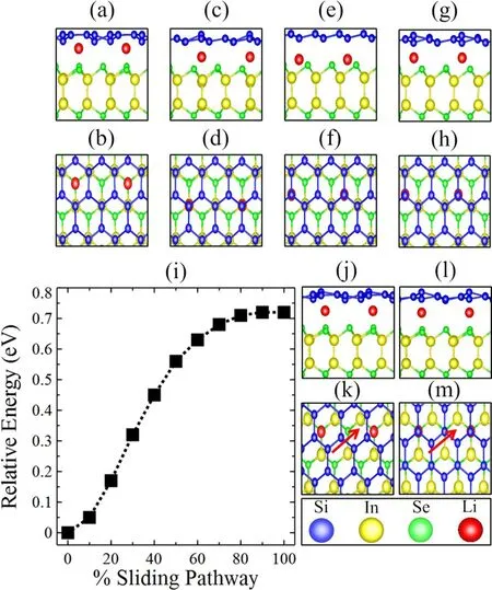
Figure 1.Side(subfigures(a),(c),(e)and(g))and top(subfigures(b),(d),(f),(h))views of silicene/InSe vdW-HS with lithium as intercalant(red balls) at various possible interfacial sites.The subfigures (a)/(b), in which Li is atop of selenium atom, is the most stable intercalated heterostructure.Subfigure(i)shows relative changes in total energy upon sliding of silicene over InSe monolayer.The subfigures(a)/(b)and(l)/(m)show the side/top view of intercalated HS before and after sliding,respectively.Configuration obtained at halfway of sliding pathway is provided as subfigure (j)/(k).The red colour arrows in subfigures (k) and (m) show the direction of sliding.
3.2.Energetics and layer sliding
After obtaining the most stable configuration of silicene/InSe vdW-HS[subfigures 1(a)/(b)],silicene is slid over the InSe layer covering a length of 2.27 Å, which is the bond length between two adjacent silicon atoms of the corrugated silicene.The sliding is carried out in ten equal parts(one part = 2.27 Å/10).The total energy is collected at the end of each sliding portion of the pathway.The subfigure 1(i) shows the relative change in total energy upon sliding of silicene over InSe in the presence of intercalant.A side/top view of the intercalated HS as it appears at the beginning[subfigures 1(a)/(b)],halfway[subfigures 1(j)/(k)]and end point [subfigures 1(l)/(m)] of the sliding pathway are shown in figure 1.The red arrows marked in subfigures 1(k)and(m)show the sliding direction.There is a continuous increase of total energy from the beginning of the sliding until around 80%of the pathway, after that the energy retains a uniform trend.
A variation of the vdW gap between the two monolayers upon sliding of silicene is also investigated,as shown in figure 2.The calculated vdW gap of most stable intercalated HS is 3.244 Å, which is significantly larger than the vdW gap(2.923 Å) belonging to unintercalated silicene/InSe HS.The vdW gap increases continuously as the sliding proceeds and reaches the maximum value (3.808 Å) at 80% of the sliding pathway.A nudged elastic band (NEB) method is employed to calculate the potential energy barrier (Eb) between two sequential divisions of sliding.Figure 3 provides the calculated Ebvalues indicated by upper case letters A,B,C,D,E,F,G,H,I and J relating to portion of the sliding pathway from 0%to 10%,10%to 20%, 20%to 30%,30%to 40%,40%to 50%, 50% to 60%, 60% to 70%, 70% to 80%, 80% to 90% and 90% to 100%, respectively.The silicene encounters the highest energy barrier (Eb= 144.14 meV) when it slides from 20% to 30% of the sliding pathway.The sliding becomes more difficult due to the hindrance caused by the presence of Li at the vdW gap as compared with the unintercalated system.
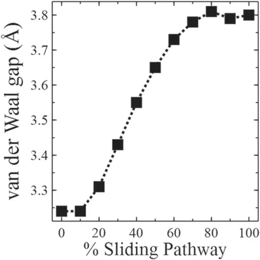
Figure 2.Variation of vdW gap as a function of the percentage of the sliding pathway.
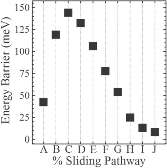
Figure 3.Calculate potential energy barrier (Eb) appeared between two consecutive divisions of the sliding pathway.Sliding is carried out in ten equal parts (one part = 2.27 Å/10).Calculated Eb values have been shown indicated by upper case letters A,B,C,D,E,F,G,H,I and J relating to portion of the sliding pathway from 0%to 10%,10%to 20%,20%to 30%,30%to 40%,40%to 50%,50%to 60%,60% to 70%, 70% to 80%, 80% to 90% and 90% to 100%,respectively.
3.3.Interfacial electronic properties
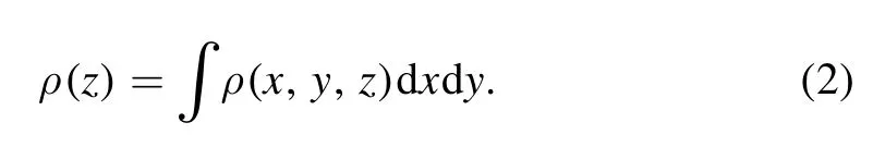
A study of the interfacial electronic properties offers a significant platform for making functional electronic devices.Various interfacial electronic properties such as planar average charge density difference (Δρ), dipole charge transfer(ΔQ) and interface dipole moment (Δμ) are calculated for intercalated silicene/InSe vdW-HS.Calculated values relating to the aforementioned properties are plotted as a function of vertical length of the supercell collected at the initial,halfway and complete sliding pathway as shown in figure 4.Each subfigure of figure 4 has dotted red and blue vertical lines, which indicate the position of InSe and silicene at the interface of the HS,respectively.Δρ(z)for intercalated HS is calculated as

where ρ(z)Li/silicene/InSe, ρ(z)silicene/InSeand ρ(z)Liare the planar average charge densities of intercalated vdW-HS,unintercalated vdW-HS, and Li, respectively.Δρ is provided along z-axis(equation (2)), whereas electron density depletion and accumulation is indicated by negative and positive values,respectively.The decrease/increase of the electron density is mainly caused as a result of the formation of heterostructure and intercalation.
Before sliding, the most stable intercalated vdW-HS has noteworthy values of ρ(z) [subfigure 4(a)] near silicene due to Li intercalation.The midway [subfigure 4(b)] and full length[subfigure 4(c)]sliding of the silicene further increased ρ(z)near the silicene.Sliding increases the internal distance between the participating layers as indicated by the enlarged width between the marked vertical red and blue dotted lines as shown in subfigures 4(b) and (c).
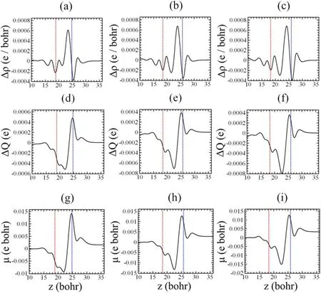
Figure 4.Calculated planar average charge density difference (Δρ), charge transfer (ΔQ) and interface dipole moment (μ) for intercalated heterostructure at initial[subfigures(a),(d),(g)],midway[(b),(e),(h)]and complete[(c),(f),(i)]coverage of the sliding pathway.Dotted red and blue vertical lines indicate the position of InSe and silicene at the interface, respectively.
Furthermore, ΔQ and μ are calculated utilizing ρ(z)through the following equations.
Interfacial electronic property ΔQ describes the direction of charge transference from InSe to silicene for negative values of ΔQ and vice versa.Before the layer sliding[subfigure 4(d)],Li transfers a reasonable amount of ΔQ to InSe.For both the halfway and complete coverage of the sliding pathway a minor decline in the positive values of ΔQ is seen near silicene as shown in subfigure 4(e) and subfigure 4(f), respectively.Interfacial electronic property μ(z) is determined by the integration (equation (4)) along the vertical length (z-axis) of the supercell.For initial [subfigure 4(g)], middle [subfigure 4(h)]and final [subfigure 4(i)] coverage of the sliding pathway,positive values of μ(z) are found near silicene possibly due to presence of Li.Plots for ΔQ and μ(z)show a similar trend with the later quantity having higher values.
Figure 5 shows band structures of intercalated silicene/InSe vdW-HS along high-symmetry directions for unslided[subfigure 5(a)] and slided [subfigure 5(b)] configurations.The sliding of silicene over InSe monolayer in the presence of Li-intercalant results in the negligible changes in the overall shape of the band structure.There is no significant band gap at Fermi level (indicated by blue horizontal line) for both slided and unslided configurations.It is worth mentioning that very few valence bands are available near fermi level that can be tuned using existing techniques.
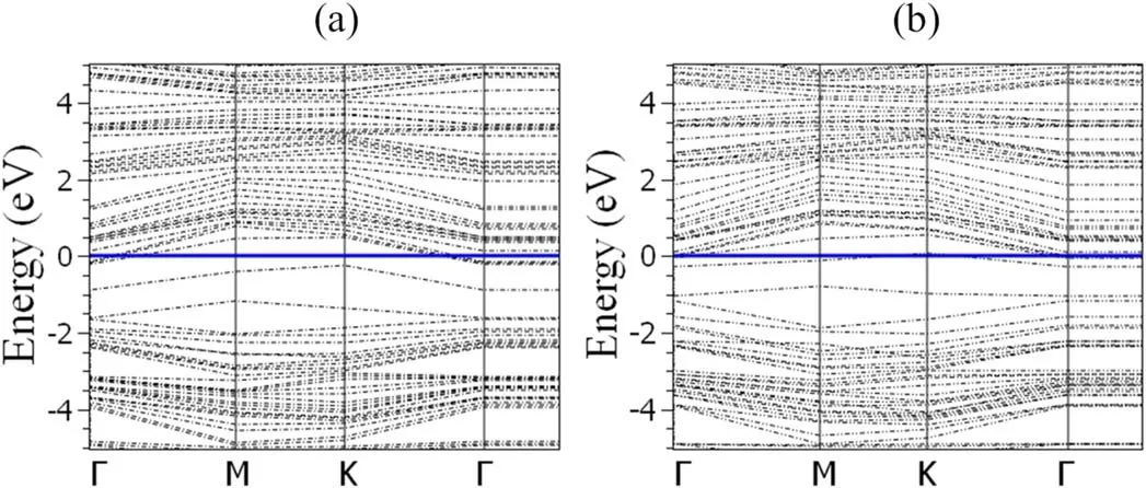
Figure 5.Calculated band structures of intercalated silicene/InSe heterostructure before (a) and after (b)sliding of silicene over InSe layer.The Fermi level is set at 0 eV indicated by a horizontal blue line on the energy scale in band structure plots.
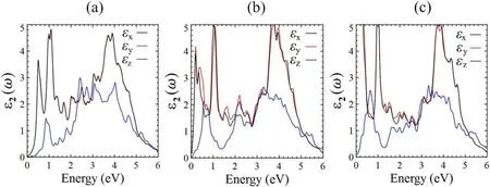
Figure 6.Calculated in-plane (εx and εy) and out-of-plane (εz) components of the dielectric function.
The dielectric function(DF)of intercalated silicene/InSe vdW-HS is examined with the help of complex DF[ε(ω) = ε1(ω) + iε2(ω)].The imaginary part [ε2(ω)] can be related to the polarization losses of the material under a symmetrical fields and can be determined as follow [37];Subfigures 6(a)–(c) describe the calculated in-plane (εxand εy) and out-of-plane (εz) dielectric functions (DFs) of Liintercalated vdW-HS at the initial, halfway and full coverage of the sliding pathway, respectively.It is clear from the figure 6 that there is a major difference between the DF along the planar and vertical direction.It is worth mentioning that as a result of the sliding, both in-plane and out-of-plane DFs associated with the intercalated vdW-HS deviates from the DFs of the starting configuration.Also,it is evident that both εxand εyare almost same in case of unslided[subfigure 6(a)]configuration and the trend is repeated for the case of the halfway and completely slided configuration.Sliding causes only minor variations in the resulting in-plane DFs in contrary to out-of-plane DFs.For in-plane DFs, significant absorption peaks are found at 1 eV and 4 eV.In case of out-of-plane DFs,noteworthy absorption region lies between 2 eV and 5 eV for configurations appearing at initial, halfway and full coverage of the sliding pathway.The response of the VdW-HS to external electromagnetic waves can be described with the help of plots (figure 6) that also forecasts electronic optical transitions (represented by peaks) between valence and conduction band giving rise to the absorption region.
4.Conclusion
Interfacial electronic properties of a two-dimensional intercalated silicene/InSe van der Waals heterostructure (vdWHS)have been calculated using density functional theory.The most stable intercalated vdW-HS is obtained by comparing energetics of various systems having different interfacial positions for Li.In order to tune the physical properties,silicene is slid over a InSe layer in regular intervals.The vdW gap increases as the sliding proceeds and reaches the maximum value of 3.81 Å.Potential energy scans along the direction of the slide reveals that sliding is required to overcome an order of higher energy due to Li atoms at the interface as compared with the unintercalated vdW-HS.The maximum energy barrier of 0.14 eV is found along the sliding pathway.Li intercalation increases average charge density difference near silicene reaching the maximum value on the completion of sliding.Electronic optical transitions representing the absorption region have been indicated by the inplane and out-of-plane dielectric function.As a result of the sliding, in-plane and out-of-plane components of the dielectric functions (DFs) associated with the intercalated vdW-HS deviates from the dielectric functions of the unslided configuration.The employed approach advocates that the physical properties of layered materials can be tuned effectively in a controlled manner through a combination of intercalation and layer sliding.
杂志排行

Communications in Theoretical Physics的其它文章
- Thermal currents obtained and mutually switched by a modified Haldane model in graphene
- Nonequilibrium effects of reactive flow based on gas kinetic theory*
- Preferential attachment network model with aging and initial attractiveness
- A classical density functional approach to depletion interaction of Lennard-Jones binary mixtures
- A residual-based message passing algorithm for constraint satisfaction problems
- Electronic structure and optical properties of non-metallic modified graphene: a firstprinciples study