Three-level LCC resonant DC-DC converter with high-gain modular
2022-02-25WUJiahuiLIUDongWANGYanboCHENZhe
WU Jiahui, LIU Dong, WANG Yanbo, CHEN Zhe
Department of Energy Technology, Aalborg University, Aalborg 9220, Denmark
[Abstract]In this article, four types of resonant converters were introduced firstly, which are series resonant converter, parallel resonant converter, series-parallel resonant converter and multi-component resonant converter.Then their merits and demerits were discussed briefly.In the meantime, the recent research status was outlined through many related papers.On this basis, a three-level (TL) series-parallel resonant converter with a structure reconfigurable control was proposed for medium voltage application with high-gain modular.Compared with the traditional resonant converter, the proposed converter has two operation configurations, which can not only satisfy the wide output range, but also shrink the switching frequency range close to the resonant frequency.And the voltage stress of primary side switch can be reduced by half thanks to the TL structure, which is beneficial to reduce the cost.Consequently, theefficiency over the wide output range can be improved.The operation principle, characteristics, and performances of the proposed converter were analyzed.Finally, the simulation results were presented to verify the effectiveness of the proposed converter.
[Key words] three-level (TL) series-parallel resonant converter; structure-reconfigurable control; high-gain modular
1 Introduction
Resonant DC/DC converters with high switching frequency have been widely applied for renewable energy systems (e.g.photovoltaic generation, electric vehicles, and energy storage system) because of its merits including galvanic isolation, wide range of zero-voltage switching (ZVS), high efficiency[1-3].In terms of the topology type of the resonant tank, the resonant converter can be classified into series resonant converter, parallel resonant converter, series-parallel resonant converter and multi-component resonant converter[4-6].Series resonant converter has fewer resonant component and simple structure, the resonant current is reduced with respect to load.However, the unified voltage gain is less than 1, which is not satisfied with the application of wide range of output voltage[7,8].Compared with the series resonant converter, parallel resonant converter overcomes the issue of voltage gain, but the efficiency is much lower thanks to larger circulation of reactive power under rated mission profile.Series-parallel resonant converter combines the advantages of previous two converters.Besides, it has fewer resonant components than multi-component resonant converter and more conducive to realize high power density.
In general, the pulse frequency modulation (PFM) control is utilized for series-parallel resonant converter to adjust the voltage gain.Renewable energy source such as photovoltaic generation and energy storage system feature a wide range of input or output voltage.Thus, wide range of switch frequency is required for these application and leads to increased switching power losses.
In order to shrink the range of switching frequency as much as possible while meeting the requirement of voltage gain.Many approaches based on new control strategies and reconfigurable structure have been proposed to solve this challenge[9-15].Ref.[9] proposes pulse width modulation (PWM) control for a series-parallel resonant converter, in which the switching frequency is fixed at the resonant frequency.In ref.[10-12], phase shift control e.g.single phase control, extended phase shift control and triple phase shift control were proposed to obtain high-gain modular.However, the wide range of ZVS characteristics of resonant converter with fixed switching frequency control would be easily lost, resulting in further decrease of efficiency and EMI problems.To reduce the power loss caused by high switching frequency, some hybrid control strategies are proposed to obtain wide voltage range with a small variation of switching frequency.In ref.[13], PWM-PFM hybrid controlled LLC resonant converter is proposed for wide range of ZVS and input voltage, PFM and PWM control are utilized for high voltage gain and low voltage gain respectively, the maximum switching frequency of the converter would be restricted as the boundary of mode transition, thus the switching frequency would not be reached so high at the lowest voltage gain.In ref.[14], an improved PWM-PFM hybrid control strategy is adopted for resonant LCC converter with double closed control-loop, the voltage outer loop is utilized to adjust the switching frequency, and the inner loop based on the calculation of the switching frequency and voltage gain is used to adjust the conduction angle simultaneously.Ref.[15] proposes a self-sustained phase-shift modulation LCC resonant converter, the resonant current is detected for achieving the inner loop control of conduction angle.However, additional control loop is needed for these hybrid control strategies, and the parameter design is complicated.
As for the reconfigurable structures to achieve wide range of voltage within small variation of switching frequency, they can be further divided into two types that are reconfigurable resonant tank and reconfigurable bridge.In order to meet the requirements of wide output range for PV system, a series resonant converter with dual-mode rectifier is proposed in ref.[16].In ref.[17], a semi-active reconfigurable rectifier is proposed, in which the proposed rectifier has the voltage-double and voltage-quadruple configuration.Similarly, a reconfigurable bridge structure with three operation configuration is proposed in ref.[18].Ref.[19] proposes a LLC resonant converter with the variable resonant frequency by utilizing two resonant tank with different resonant parameters.In ref.[20], an improved LLC converter is proposed, in which four different operation configurations can be realized by adjusting the turns ratio of the transformer.However, this kind of topology has less cost.
In the above structure-configurable resonant converters[16-20],the primary-side power devices need to withstand the whole input voltage, which makes them not suitable for the high input voltage applications.Accordingly, a three-level (TL) LCC resonant converter with the structure-configurable control is proposed in this paper for the high input voltage and wide range of output applications.There are two operation configurations in the proposed converter, which can thus not only extend the adjustable output voltage range, but also shrink the switching frequency close to the resonant frequency.Accordingly, the efficiency over the wide output range can be improved.The operation principle, performances, and the effectiveness of the proposed converter with the structure-configurable control is verified by the simulation results.
2 Circuit topology and operation priciple
2.1 Circuit topology
The circuit topology of the proposed TL LCC resonant converter is shown as Fig.1.In Fig.1, two input capacitorsCi1andCi2are in series to split the input voltageVininto two voltagesV1andV2;S1/D1~S8/D8are primary-side power devices;Cs1andCs2are two clamping capacitors;D9~D12are four clamping diodes;C1~C8are parasitic capacitors ofS1/D1~S8/D8;Lr,CpandCrare resonant inductor and capacitors,Lris composed of an external independent inductor plus transformer leakage inductance.In order to make full use of transformer leakage inductance,Cpis connected in parallel with the secondary side of the transformer;Dr1~Dr4are secondary-side rectifier diodes;Cois the output filter capacitor.Besides,Vabis the voltage between pointaandb;ipis the primary current throughLr;iCp,vCpis the current throughCpand the voltage onCprespectively;vCris the voltage onCr;io1andioare the output current beforeCoand afterCorespectively.
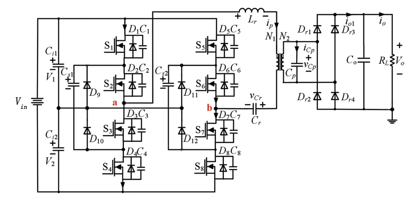
Fig.1 The circuit Topology
2.2 Operation principle
In order to simplify the following analysis, some assumptions are made below:
1) Input capacitorsCi1,Ci2and clamping capacitorsCs1,Cs2are large enough to be considered as the voltage sources with the value ofVin/2;
2) The output filer capacitorCois large enough to be considered as the voltage source;
3) The parasitic capacitorsC1~C8have the same value namedCeq;
4) The short period of the primary voltageVabwith the high voltageVincan be neglected in the configuration Ⅱ.
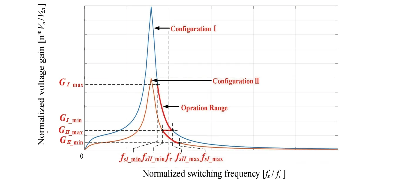
There are two working configurations of the proposed TL LCC DC/DC converter to satisfy the wide output range.Fig.2(a) and 2(b) show the operation principle of the configuration Ⅰ and Ⅱ respectively.In Fig.2,drv1~drv8are the driving signals for the power devicesS1/D1~S8/D8;Tsis the switching period; and (drv1,drv4), (drv2,drv3), (drv5,drv8), (drv6,drv7) are complementary.The output voltageVois adjusted by changing the switching frequencyfs.In the configuration I,drv1~drv8are all 0.5*Tsif neglecting the dead time, the primary voltage of the transformerVabisVinand -Vin.In the configuration Ⅱ,drv1,drv4are 0, which means the switches ofS1andS4are turned off during the entire switching cycle,anddrv2drv3,drv5,drv6,drv7,drv8are all 0.5*Tsif neglecting the dead time, the primary voltage of the transformerVabisVin/2 and -Vin/2.Therefore, the voltage gain in the configuration I is twice of that in the configuration Ⅱ under the same operation conditions.
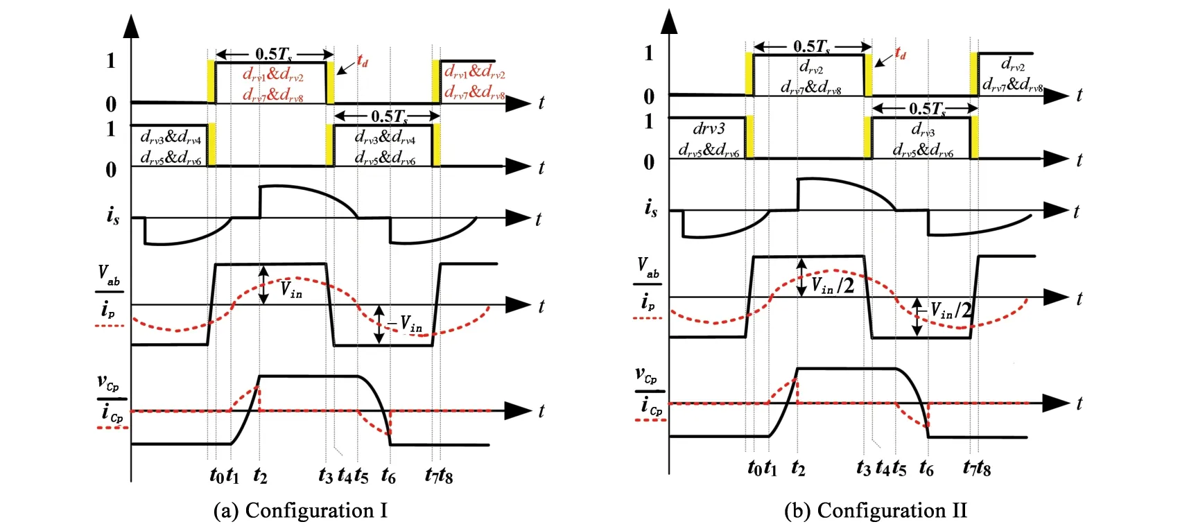
Fig.2 The operation principle
Fig.3 shows the equivalent circuits in the configuration Ⅰ when the switching frequencyfsequals to the resonant frequencyfrif neglecting the dead time.The resonant frequencyfrcan be obtained by (1):
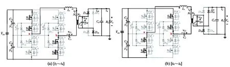
Fig.3 The equivalent circuits in the configuration Ⅰ
(1)
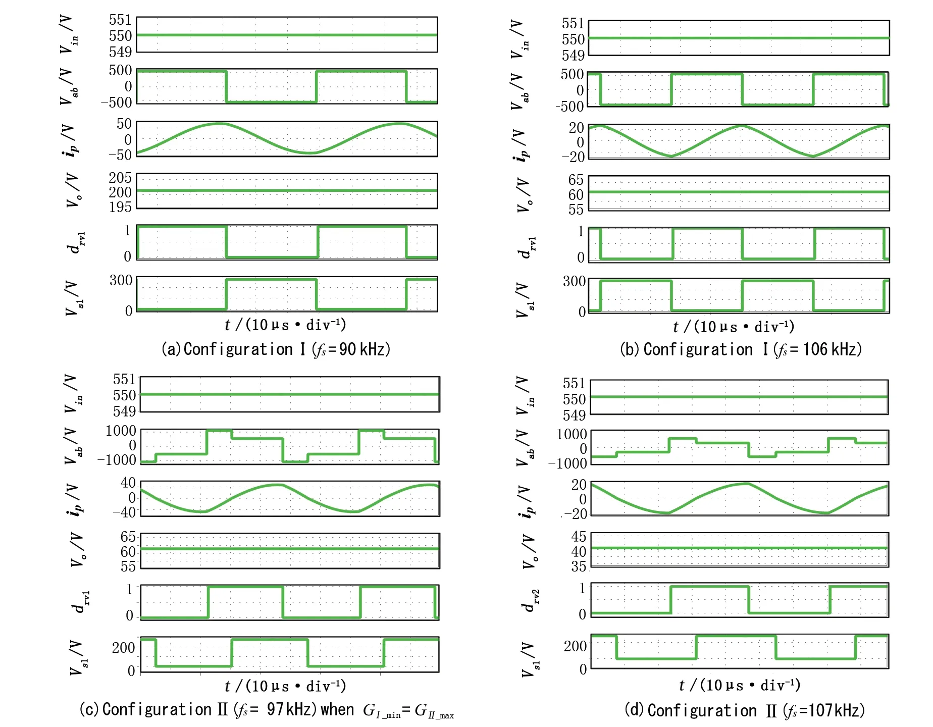
The analysis of other operation conditions (fs>frandfs Stage 0 [beforet0]:the switchesS3,S4,S5, andS6are all in on-state.The primary currentipis negative.During this stage, the voltage on the paralleled capacitorCpis -Vo, so the current of secondary sideisdecrease linearly.The primary voltageVabis -Vin.The output rectifier diodesDr2andDr3conduct to transfer the power to the load. Stage 1 [t0~t1]:Att0, the switchesS1,S2,S7andS8turn on with zero voltage state because their body diodes are all in on-state beforet0, and the switchesS3,S4,S5,S6are turned off.The primary voltageVabchanges toVin.The output rectifier diodesDr2,Dr3turn off andDr1,Dr4turn on.During this stage,vCpisVo, so the current of secondary sideisincreases linearly.isincreases to 0A att1. Stage 2 [t1~t2]:Att1, all of the rectifier diodes of secondary side turn off, the paralleled capacitorCpis charged by the resonant currentiCpfrom the primary side.The voltage onCpincreases from -Voand reachesVoatt2.And the current through theCpincreases and reaches the peak current att2.During this stage, the output voltage is supported by the output capacitorCo. Stage 3 [t2~t3]:Att2, the voltage on the paralleled capacitorCpis equal to the output voltage, the rectifier diodesDr1andDr4turn on.The current of primary sideipis positive and decreases to 0A att3.During this stage, the energy is transformed from primary side to secondary side Att3, the next switching period starts.The related analysis is the same as that of [t0~t3], which is not repeated here. Fig.4 shows the equivalent circuits in the configuration Ⅱ when the switching frequencyfsequals to the resonant frequencyfr.The analysis of other operation conditions (fs>frandfs Fig.4 The equivalent circuits in the configuration Ⅱ Stage 0 [beforet0]:the switchesS3,S5, andS6are all in on-state.The primary currentipis negative.During this stage, the voltage on the paralleled capacitorCpis -Vo, so the current of secondary sideisdecreases linearly.The primary voltageVabis -Vin/2.The output rectifier diodesDr2andDr3conduct to transfer the power to the load. Stage 1 [t0~t1]:Att0, the switchesS2,S7andS8turn on with zero voltage state because their body diodes are all in on-state beforet0, and the switchesS1,S3,S4,S5,S6are turned off.The primary voltageVabchanges toVin/2.The output rectifier diodesDr2,Dr3turn off andDr1,Dr4turn on.During this stage,vCpisVo, so the current of secondary sideisincreases linearly.isincreases to 0A att1. Stage 2 [t1~t2]:Att1, all of the rectifier diodes of secondary side turn off, the paralleled capacitorCpis charged by the resonant currentiCpfrom the primary side.The voltage onCpincreases from -Voand reachesVoatt2.And the current through theCpincreases and reaches the peak current att2.During this stage, the output voltage is supported by the output capacitorCo. Stage 3 [t2~t3]:Att2, the voltage on the paralleled capacitorCpis equal to the output voltage, the rectifier diodesDr1andDr4turn on.The current of primary sideipis positive and decreases to 0A att3.During this stage, the energy is transformed from primary side to secondary side Att3, the next switching period starts.The related analysis is the same as that of [t0~t3], which is not repeated here. Before analyzing the voltage gain, the following parameters are defined in the equations(2), (3), and(4): (2) (3) (4) (5) In (2)~(4),Rois the load resistance,Reis the reflected load resistance,Qis the quality factor, andmis the capacitance ratio. When the converter operates in the configuration I, the primary voltageVabisVinand -Vin, so the normalized voltage gain namedG_Ican be obtained by (6) according to the first harmonic approximation (FHA) method: (6) When the converter operates in the configuration Ⅱ, the primary voltageVabisVin/2 and -Vin/2, so the normalized voltage gain namedG_Ⅱcan be obtained by (7) according to the FHA method: (7) Fig.5 shows the normalized voltage gain curves of the two operation configurations when having the constant output resistance. From Fig.5, the following points can be observed: Fig.5 The normalized voltage gain curves under two configurations and operation range 1) The voltage gain range can be extended by changing the two operation configurations; 2) A wider output voltage range can be achieved within a narrow switching frequency that is close to the resonant frequency. It needs to be mentioned that the minimum voltage gain of the configuration I should be equal to or smaller than the maximum voltage gain of the configuration Ⅱ to ensure the output voltage changing smoothly. The operation range with the switching frequency range are marked by the red color line in Fig.5. Under the configuration I, the range of the normalized voltage gain is fromGI_maxtoGI_ minand the range of the normalized switching frequency is fromfsI_mintofsI_max.The configuration I is used for the highly required output voltage.The output voltage can be reduced by increasing the switching frequency. The configuration Ⅱ starts to be utilized to further reduce the output voltage when the voltage gain declines toGI_min.Under the configuration Ⅱ, the range of the normalized voltage gain is fromGⅡ_ maxtoGⅡ_ minand the normalized switching frequency is fromfsⅡ_ mintofsⅡ_ max. Based on the above analysis, it can be concluded that the proposed structure-reconfigurable control can not only extend the total range of the normalized voltage to [GⅡ_ mintoGI_ max], but also squeeze the total range of switching frequency which is near the resonant switching frequency. The soft-switching performance of the proposed converter is the same as that of the conventional LCC resonant converter.The primary-side power switches can achieve the ZVS in the entire operation range in the proposed converter.The secondary-side rectifier diodes can achieve the ZCS when the switching frequency is the same as and smaller than the resonant frequency. Firstly, the required peak voltage gain should be included in the designed operation range of voltage gain, which means that the following equation (8) should be also fulfilled: (8) Based on (8), the actual range of switch frequency [fsI_min,fsⅡ_max] can be obtained. Then, the switching frequency at the mode transition point namelyfs_twill be selected belowfⅡ_max.In order to ensure the transition between the configuration I and Ⅱ smoothly, the equation (9) should be fulfilled: G_I(m,fs_t,Q)=G_Ⅱ(m,fs_t,Q) (9) Besides, the voltage gain at the mode transition can be obtained based on (9). In order to verify the proposed converter with the structure-reconfigurable control, a simulation model is established in PLECS, whose circuit parameters are shown in Appendix. Fig.6 presents the simulation results in two configurations.From Fig.6, it can be observed that: Fig.6 The simulation results in two configurations 1) the output voltageVocan be adjusted to be 200V and 400V as shown in Figs.6(a) and 6(d), which means that the voltage gain would be 2 and 0.4; 2) the output voltageVocan be adjusted to be both 60V in the configuration Ⅰ (fsis 106kHz) and configuration Ⅱ (fs= 97kHz) as shown in Figs.6(b) and 9(c), which means the transition between two configurations would be seamless. It needs to be mentioned that there exists an error in the switching frequency corresponding to the voltage gain when comparing the simulation results with theoretical calculations, especially under the operating condition that the switching frequency is far from the resonance frequency.The reason of causing this error is that the current distortion affects the accuracy of FHA. This paper proposes a TL series-paralleled LCC resonant DC/DC converter with the structure-reconfigurable control for the wide output range and high input voltage applications.There are two operation configurations in the proposed converter.By utilizing these two configurations, the wider output voltage range can be realized under the squeezed switching frequency range near the resonant frequency in comparison with the conventional resonant converter with only PFM control.Consequently, the efficiency over the wide output range can be improved.Finally, the simulation results are demonstrated to verify the effectiveness of the proposed converter with the structure-reconfigurable control. Table 1 shows the circuits parameters of the established simulation model. Table 1 The circuit parameters of the established simulation model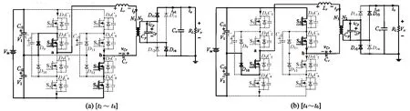
3 Characteristics and performance
3.1 Voltage gain
3.2 Mode transition and control
3.3 Soft-switching performance
3.4 Mode transition design
4 Simulation verification
5 Conclusion

杂志排行

长江大学学报(自科版)的其它文章
- 压裂液在火山岩不同类型孔隙中的分布特征
—— 以新疆西泉井区火山岩油藏为例 - 基于高阶统计量的砂泥岩薄互层油气检测方法
- Analysis of the line current differential protection considering inverter-interfaced generation station and countermeasures
- Balanced-switch-current-based modulation strategy for a three-level DC/DC converter with input-parallel-output-parallel structure
- 基于三维连井剖面的地层抗钻特性参数评价
——以珠江口盆地陆丰区块为例 - 考虑滑移效应的页岩基质纳米孔隙中压裂液滤失速度分形计算新模型