Mechanism of microweld formation and breakage during Cu–Cu wire bonding investigated by molecular dynamics simulation
2022-01-23BeikangGu顾倍康ShengnanShen申胜男andHuiLi李辉
Beikang Gu(顾倍康) Shengnan Shen(申胜男) and Hui Li(李辉)
1School of Power and Mechanical Engineering,Wuhan University,Wuhan 430072,China
2The Institute of Technological Sciences,Wuhan University,Wuhan 430072,China
Keywords: Cu-Cu wire bonding,bonding mechanism,atomic stress,molecular dynamics simulation
1. Introduction
Currently, wire bonding is the most popular first-level interconnection technology used between the die and package terminals.[1]It has been widely used as an interconnection technique in the electronic packaging industry since it was invented in the 1960s.[2]Approximately 9 trillion wires in electronic devices were bonded globally by this technique in 2008.[3]Owing to the cost and flexibility, it will still play an important role for a long period.[4]Recently, gold has been extensively used in wire bonding because of its excellent performance.[5]Conversely,copper wire exhibits better tensile strength and lower cost compared with gold wire, increasing its use as a substitute for gold wire.[6]Nonetheless,it presents several drawbacks owing to its oxidation, high strength, and high hardness.[7]Therefore, the bonding mechanism of copper needs to be further evaluated.
Despite its long-term and excessive usage,the wire bonding mechanisms have not been completely evaluated,[8]and the fundamental research is still required. From the chemical point of view, the wire bonding mechanism consists of the formation of solid-state metallic bonds between the surfaces of wire and substrate to achieve the required connecting strength.[9]Several methods have been used to form metal bonds that meet the bonding conditions,such as the ultrasonic wire bonding. In this method,the ultrasonic energy is applied onto the contact interface to break the oxide films presented on the surface of the wire and substrate,[10]which gets metal atoms close enough to build metal bonds. In the past, experimental methods were used to analyze the changes;[8]however, these methods presented drawbacks like being destructive and were not able to detect microscale changes.[11]Because of that,it is difficult to identify the changes in the reaction zone between the contact surfaces. Therefore,simulation is the only possible approach to evaluate the wire bonding.Although finite-element(FE)simulations are widely used to predict mechanical behavior, the results depend on phenomenological models, which rely on experimental observations and practical inverse analysis of the bulk behavioral laws.[12]However,experimental data are difficult to obtain,and some macro mechanisms are no longer applicable from the micro perspective, hindering the use of the FE method to perform simulations with acceptable quality. Dinget al.[13]and Ding and Kim[14]established a 3D model and a 2D model to analyze the contact pressure and temperature rise on the contact surface,in which only the normal force was considered and the vibration was coarsely added in the analysis. The result showed that the largest contact pressure was located at the interface perimeter, which disagrees with the result reported by Winchell and Berg.[15]Consequently, a microscale approach is needed to deal with this problem.
Molecular dynamics (MD) simulation is more appropriate to investigate the local changes of microwelds as the changes of microwelds occur at an atomic level. Per-atom modeling,simple and accurate kinematic equations,complete and reliable potential function, and not high computational workload make MD suitable for studying the behavior of metal systems. Dinget al.[16]simulated the interfacial contact in Au-Au ultrasonic wire bonding and adhesion in pull test of the weld and obtained the estimated tensile strength. Longet al.investigated the evolution of surface morphology in the friction process based on the nano-friction model and discovered that the weld can be formed or broken instantly.[8]However,atomic stress analysis during the wire bonding process has not been evaluated yet. It is necessary to study the atomic stress during the contact process of Cu-Cu wire bonding, which is helpful to understand the mechanism of wire bonding and get better bonding parameters.
In this study, the contact model for the nanoindentation process between the wire and substrate was developed to simulate the contact process of the Cu wire and Cu substrate. The mechanism of microweld formation and breakage during Cu-Cu wire bonding was investigated by MD simulation. The evolution of the indentation morphology and distribution of the atomic stress were investigated through the loading and unloading processes.
2. Molecular dynamics modeling
All the mechanical behaviors involved in this study were performed in the large-scale atomic/molecular massively parallel simulator (LAMMPS)[17]and employed a simulation time step of 0.01 ps. The model was visually analyzed by using the open visualization tool(OVITO).[18]The embeddedatom method,which was developed by Daw and Baskes,[19,20]was applied to govern the energetics and dynamics of all the Cu atoms in every layer of the model. The total potential energyEof a single atomiis calculated as follows:
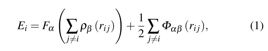
whereFis the embedding energy, which is a function of the atomic electron densityρ,Φis a pair potential interaction,andαandβare the element types ofiandjatoms, respectively.Both sums in the formula are over all atomineighbors within the cutoff distance. In this work,the potential parameters are contributed by Foileset al.[21]
In this study, a local part of the wire and corresponding local part of the substrate were developed to model the nanoindentation,contact,and separation of the wire and substrate.[8]The basic geometry of the model is shown in Fig. 1. There are two parts in the model: Cu wire and Cu substrate. The Cu wire consists of two different layers: a sliding layer and a Newton layer. The Cu substrate consists of three different layers: a sliding layer, a thermo-layer, and a Newton layer. The Newton layers perform the contact behavior during the simulation with the NVE ensemble. The sliding layers were used to provide the desired displacements. In the Cu wire,the sliding layer was used to make the indenter move correctly. In the Cu substrate, the sliding layer was used to fix the bottom of the model,and the velocity of the atoms in sliding layer is set to be 0 m/s. The thermo-layer was used to control the temperature with the NVT ensemble (constant number of atoms,volume, and temperature).[22]The initial temperature of the thermo-layer was set at 0.1 K and kept during the whole process because the fluctuations of the atomic stress distributions due to the thermal effects can be significantly decreased.[23]
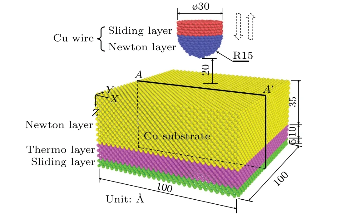
Fig.1. Geometries of the Cu-Cu wire bonding models.
According to previous studies,[24,25]the indentation speed of 10 m/s was used in this simulation. Prior to the indentation process, the system was allowed to have 100 ps of relaxation to decrease its energy. The nanoindentation process consists of two steps: the loading and unloading processes.Firstly, during the loading process, a speed of 10 m/s was added to the Cu wire part(indenter)to move it along the negative direction of theZ-axis toward the Cu substrate by 30 ˚A.Secondly,during the unloading process,the Cu wire part(indenter) was added at a speed of 10 m/s to move it along the positive direction of theZ-axis and separate it from the Cu substrate by 30 ˚A. The loading force was calculated by summing the atomic forces of Newton layer atoms of the Cu wire part in theZdirection. Because the indenter deforms, theZ-coordinate of the vertex was taken when the indenter was not deformed as the abscissa of the load-depth curve. For the atomic stress analysis,the six components of the atomic stress tensor were calculated based on the spatial and temporal ensemble averages of the atomic virial stress[8,26]

whereσvm(i)is the von Mises stress of atomi,andσmn(i)is the atomic stress tensor in the order ofm,n(x,y,orz).
3. Results and discussion
3.1. Indentation and retraction
Figure 2 shows an atomic[010]slice of the Cu wire and substrate during the loading and unloading processes. An attractive force between the wire and the substrate is observed when the wire is close to the substrate, which displays the bulging of the substrate surface atoms under the wire tip, as shown in Fig.2(a). The attraction force increases with the decrease of the distance between the substrate and wire.The substrate surface atoms are rapidly contacted by the wire atoms,as shown in Fig. 2(b). As the wire continues to press downward, the repulsion between the substrate and wire becomes the main force. Because the substrate atoms are compressed at the lower end of the wire,the atomic lattice begins to deform and the strain energy increases. When the repulsion exceeds a certain value, the lattice structure breaks, and the substrate atoms start to rearrange and the strain energy is released, as shown in Fig. 2(c). During the unloading process, the main force acting on the substrate atoms changes from repulsion to attraction.Upon retraction of the wire away from the substrate surface, a small portion of the substrate atoms adheres to the indenter surface,as shown in Fig.2(d). Continuing the retraction of the wire, a neckband is formed between the indenter and substrate,as shown in Fig.2(e). At the time of 484 ps,the wire separates from the substrate,as shown in Fig.2(f).
The variations of the Cu wire load force versus the model indentation displacement are shown in Fig. 3, which consists of the load-distance curve and unload-distance curve. During the initial contact stage,in which the indentation displacement is-3.6 ˚A,the attractive force between the wire and substrate appears and increases significantly. This instability corresponds to the jump-to-contact(JC)phenomenon.[27]During the JC process,the kinetic temperature of the system increases due to the bulging of the surface atoms, then this temperature rise is dissipated to the ambiance through stochastic collisions. At the onset of contact formation, in which the tip approach is-0.75 ˚A, the maximum attractive force reaches a value of 23.5 nN. As the indentation displacement continues to increase, the repulsive force increases and becomes the main force. When the indentation displacement equals to 2.32 ˚A,the contact load is approximately zero, and the attractive and repulsive forces between the wire and substrate achieve the equilibrium point. Further indenting the wire to the substrate, the contact load increases linearly by increasing the indentation displacement. When the indentation displacement reaches 4.50 ˚A,it meets the yielding point and the plastic deformation starts. During the unloading process, the repulsive force considerably decreases and changes to attractive force as the indentation displacement reaches 4.57 ˚A.The loading and unloading curves do not coincide,and the unloading curve presents hysteresis. This is explained by the wire indenter retraction away from the substrate, that is, a neckband forms and breaks between the indenter and substrate because of the adhesion force,as shown in Fig.2(f).

Fig.2. Atomic configurations of loading and unloading.
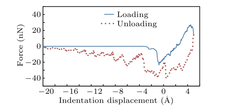
Fig.3. Load force of the Cu wire versus indentation displacement.
3.2. Analysis of indentation morphology
To evaluate the deformation behavior of the contact surface,the indentation morphology at the atomic level is investigated. Figure 4 shows the indentation morphologies of the model during the loading and unloading processes. The color change corresponds to the change in atomic displacement.Blue color represents atoms without movement(0 ˚A),and red color represents atoms that moved furthest(1 ˚A).Atoms near the contact region of the wire and substrate change from blue to red,indicating the generation of deformations. Corresponding to the load force of the Cu wire versus the indentation displacement curve, when the indentation displacement reaches-1.0 ˚A, the attractive force makes the atoms on the surface bulging and bonded together.With the increase of the indentation displacement, the repulsive force increases, and the attractive force decreases; therefore, the atomic displacement decreases. For the substrate, when the indentation displacement reaches 2.6 ˚A,the atomic displacement of the substrate reaches approximately 0 ˚A, due to the equilibrium of the attractive and repulsive forces. After that, the substrate atomic displacement increases by increasing the indentation displacement. For the wire,the atomic displacement of the wire firstly increases because of the attractive force. Thus,it reduces because of the attraction and repulsion equilibrium. After the indentation displacement reaches 2.6 ˚A,dislocations in the middle area of the Cu wire slice are observed and the atomic displacement of the wire increases by increasing the indentation displacement.
During the unloading process,the total force acting on the substrate atoms changes from repulsion to attraction with the continuation of the unloading. The repulsive force at the indentation displacement of 4.3 ˚A is smaller than that of 4.6 ˚A.Moreover,the substrate deformation near the contact region at the indentation displacement of 4.3 ˚A is smaller than that of 4.6 ˚A.There are still dislocations in the wire at the indentation displacement from 4.3 ˚A to 2.9 ˚A. By continuing to retract the wire, the main force changes to an attractive force. The deformation of the substrate near the contact region increases by increasing the attractive force. At the indentation displacement of 2.0 ˚A, the wire atoms start to rearrange, the strain energy is released, and the deformation of the substrate near the contact region reduces. At the indentation displacement of 1.0 ˚A,the strain energy in the wire fails to rearrange the atoms,and dislocations are generated in the atomic lattice. After retracting the indentation displacement to-2.3 ˚A,a neckband is formed between the wire and substrate. The deformation near the contact region increases by increasing the attractive force.
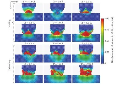
Fig.4. Atomic[010]slice of the indentation morphology during the loading and unloading processes.
3.3. Analysis of the atomic stress distribution
Figure 5 shows the contours of von Mises stress on the slice of atomic [010]. During the loading process, the main force acting on the substrate atoms changes from attraction to repulsion. For the substrate, an indentation displacement of-1.0 ˚A is observed. The maximum von Mises stress on the substrate is under the wire and close to the surface. This is because the attractive force between the wire and substrate appears and increases significantly during the initial contact stage. As the indentation displacement continues to increase,the equivalent von Mises stress at the contact edges of the substrate is higher than that at the center of contact. For the wire,after the indentation displacement reaches 2.8 ˚A,dislocations in the middle area of the Cu wire are observed. Therefore,the stress concentration occurs around dislocations.
During the unloading process, the equivalent von Mises stress value in the substrate firstly reduces and then increases.This is because the total force acting on the substrate atoms changes from repulsion to attraction with the continuation of the unloading. Stress concentration is observed in the wire because of the dislocations.
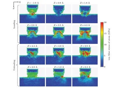
Fig.5. Contours of the equivalent von Mises stress on the slice of atomic[010].
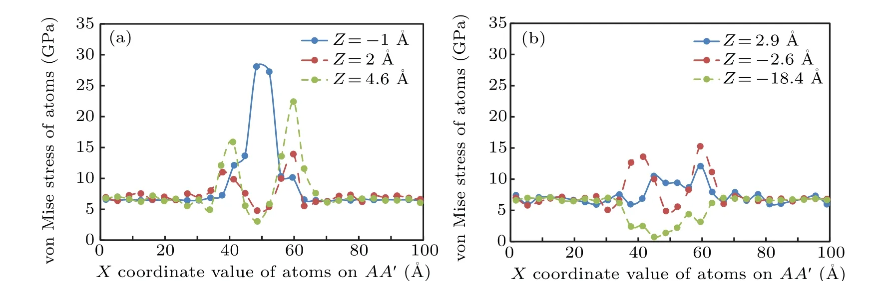
Fig.6. Equivalent von Mises stress distribution along the line AA′ of the substrate during the(a)loading process and(b)unloading process.
Figure 6 shows the equivalent von Mises stress distribution along the lineAA′of the substrate during the loading and unloading processes. During the loading process, at the indentation displacement of-1.0 ˚A,the maximum von Mises is under the wire tip;moreover,it is under the JC process and the main force is attractive. As the indentation displacement increases from 2.0 ˚A to 4.6 ˚A,the main force changes to a repulsive force.The maximum von Mises stress increases and shifts toward the edge of the contact area,as shown in Fig.6(a).During the unloading process,the main force changes from repulsive to attractive. As retracting the indentation displacement from 2.9 ˚A to-2.6 ˚A,the main force is the attraction force,as displayed in Fig.3. The maximum von Mises stress increases by increasing the attractive force. It is higher at the contact edges of the substrate than at the center of contact, as shown in Fig. 6(b). At the indentation displacement of-18.4 ˚A, a neckband forms and breaks between the wire and substrate.The minimum von Mises stress is observed under the wire tip,corresponding to the narrowest band.
4. Conclusions
In this study,a MD nanoindentation model of weld in the wire bonding process was developed. Through the loading and unloading processes, the mechanism of the Cu wire and Cu substrate contact was investigated by using the analysis of load force versus the indentation displacement curve,indentation morphology,and atomic stress distribution.The following conclusions could be drawn:
(1)During the loading process,at the initial contact stage,the main force was an attractive force because of the wire and substrate adhesion.At the indentation displacement of 2.32 ˚A,the contact load was zero. Further indenting the wire to the substrate, the main force changed to repulsive. During the unloading process,the repulsive force decreased significantly,changing to an attractive force. The loading and unloading curves did not coincide, and the unloading curve exhibited hysteresis.
(2) For the substrate, at the initial contact stage of the loading process, the maximum von Mises is under the tip of the wire.As increasing the indentation displacement,the maximum von Mises stress is increased and shift toward the edge of the contact area.The equivalent von Mises stress at the contact edges of the substrate is higher than that at the center of contact. During the unloading process,the value of equivalent von Mises stress in the substrate is reduced firstly and then increased. And it is higher at the contact edges of the substrate than that at the center of contact. There is the minimum von Mises stress at the indentation displacement of-18.4 ˚A,corresponding to the most narrow band.
(3) For the wire, stress concentration occurs around dislocations in the middle area of the Cu wire during the loading and unloading process.
(4)Microwelds can be formed and broken in an extremely short time.The attractive force between the two parts occurred and created bonds at the initial stage of contact between the wire and substrate.
Acknowledgements
Project supported by the National Key R&D Program of China (Grant No. 2019YFB1704600) and the Hubei Provincial Natural Science Foundation of China (Grant No.2020CFA032).
猜你喜欢
杂志排行

Chinese Physics B的其它文章
- Role of compositional changes on thermal,magnetic,and mechanical properties of Fe–P–C-based amorphous alloys
- Substrate tuned reconstructed polymerization of naphthalocyanine on Ag(110)
- Anti-PT-symmetric Kerr gyroscope
- Information flow between stock markets:A Koopman decomposition approach
- Cascading failures of overload behaviors using a new coupled network model between edges
- High efficiency ETM-free perovskite cell composed of CuSCN and increasing gradient CH3NH3PbI3