Simulation of X-ray-induced EMI Environment in Shell of SIP
2021-12-15CHENJinghuiZENGChao
CHEN Jinghui, ZENG Chao
(Institute of Electronic Engineering, China Academy of Engineering Physics, Mianyang 621900, China)
Abstract: This article aims to evaluate the electromagnetic interference (EMI) environment in the shell of a system in package (SIP) while irradiated by a pulsed X-ray fluecne. First, the yields and energy spectra of photoelectrons induced by X-ray were calculated using Monte Carlo numerical simulations. These results were used to simulate the self-consistent movement of photoelectrons emitting from the Kovar alloy shell and the dielectrical material of printed circuit board (PCB). The electromagnetic pulse (EMP) generated by these photoelectrons were calculated using finite difference time-domain (FDTD) method and particle-in-cell (PIC) method. An analysis of the EMI environment in the shell of SIP was performed by numerical results. It is shown that the EMI environment adjacent to the emission surfaces turns more severe because of the movement of photoelectrons. And most of the radiation energy is located at low-frequency parts, which depends on the characteristic time of X-ray. Also, reducing the area of surfaces illuminated by X-ray and the height of SIP can lessen the threat from EMI.
Key words:system in package; electromagnetic interference; X-ray
1 Introduction
System in package (SIP) as a form of a system integration package, mingles different types of elements in a package by different techniques, consisting of different types of chips and can achieve the function of system. When exposing a SIP to the X-ray environment, electromagnetic pulse (EMP) generated by photoelectrons could act as the electromagnetic interference (EMI) inducing upsets or burnout of SIP[1-2].
Different from the common EMI environment, the radiation sources of X-ray-induced EMI environment are photoelectrons emitting from metal or dielectrical material of SIP, and techniques developed to lessen the common EMI threat may have limits to the EMI environment induced by X-ray.
The EMI environment of SIP under X-ray irradiation is similar to the cavity system-generated electromagnetic pulses (SGEMP) (one of the SGEMP effects). The cavity SGEMP is the EMP environment generated by the motion of photoelectrons in the cavity of electric equipment, which excited by the irradiation of X-ray[3]. However, being different from the cavity SGEMP, the shell of SIP is much smaller, and there are chips or circuit boards inside. Furthermore, photoelectrons can not only exit from the SIP shell, but also from the surface of the dielectric material, and the photoelectrons adjacent to the surface of circuits could affect the system directly. For the reasons above, attention must be paid to not only the distribution of EMP, but also the distribution of space charges.
This study presents a numerical method to estimate the EMI environment induced by the X-ray, the time-domain and frequency-domain characteristics of EMI are also discussed in this paper.
2 Theory and calculation method
Starting from the theory of X-ray excited photoelectron, a theoretical model of EMI environment is established based on electromagnetic theory, and numerical methods are applied to calculate the distribution of EMP and charges in the shell of SIP.
2.1 Photoelectron yield of different materials
Photoelectrons in a SIP consist of the electrons emitting from Kovar alloy shell and dielectrical material of print circuit board (PCB).
The yields and energy spectra of the electrons could be acquired using Monte Carlo numerical simulation, and the emitting angle of photoelectrons obeys cosine distribution approximately.
2.2 Radiation source for EMI environment
The EMI environment is generated by the photoelectrons transfer processes, described by solving the Newton-Lorentz equations of motion as[4-5]:
(1)
(2)
Whereγis the Lorenz factor,tis the time,Eis electric field,Bis the magnetic flux density,m0,q,randvare the static mass, charge, position and velocity of the electron, respectively. Boris method, which divides the transfer process into three separate stages, was applied to solve these equations, and the accelerations caused by the electric fields and the rotation caused by the magnetic fields are calculated respectively[6].
The moving photoelectrons form space currents act as the sources of EMP, and these sources can be acquired by solving the continuity equation as:
(3)
Whereρis charge density,Jis current density. The trajectory of a macro-particle is needed to solve the continuity equation. Conventionally, the trajectory is assumed to be a straight line[7]. However, the calculation will be extremely complex for a particle crossing several cells within one step. Therefore, a fast algorithm developed by Umeda is applied to solve the continuity equation, which assumes the trajectory of a particle to be a zigzag line, and shown in Fig.1. This method has an advantage in computation speed without substantial distortion of physics[8].

The solid arrows represent particle trajectories, the dashed lines represent cell meshesFig.1 Particle trajectory for three-dimensional zigzag scheme
Once the current densityJin Eq. (3) is acquired, one could calculate the EMI environment in the shell of SIP by solving Maxwell’s equations.
(4)
WhereHis the magnetic field,Dis the electric flux density.
Considering the change of medium on the surfaces of PCB, in that case, integral equations instead of differential equations are applied to calculate the EMP, and the integral path is shown in Fig.2. One of the Maxwell integral equations is shown as follow:
(5)
WhereSis the integral surface,εis the dielectric constant of PCB,lis the integral path.
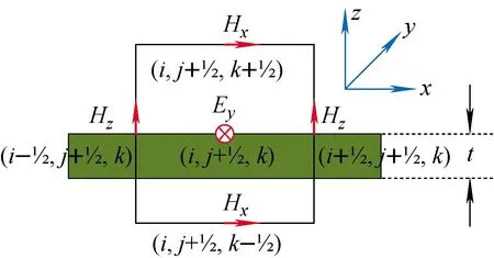
The t is the thickness of dielectric plateFig.2 Mesh of surface of dielectric material
3 Computation result
As shown in Fig.3, the typical construction of SIP is a small flat rectangular box, with a piece of single layer PCB lay on the bottom. The length of each edge of this Kovar alloy shell is 5 cm and the height is 3 cm, the thickness of the shell is 0.1 mm. The size of PCB is the same as the shell and the thickness is 2 mm. To simplify the simulation, we ignored the circuit lands and the elements on PCB. The typical elements of Kovar alloy shell are shown in Table 1. Besides, the base material of PCB is assumed to be polytetrafluoroethylene (PTFE).
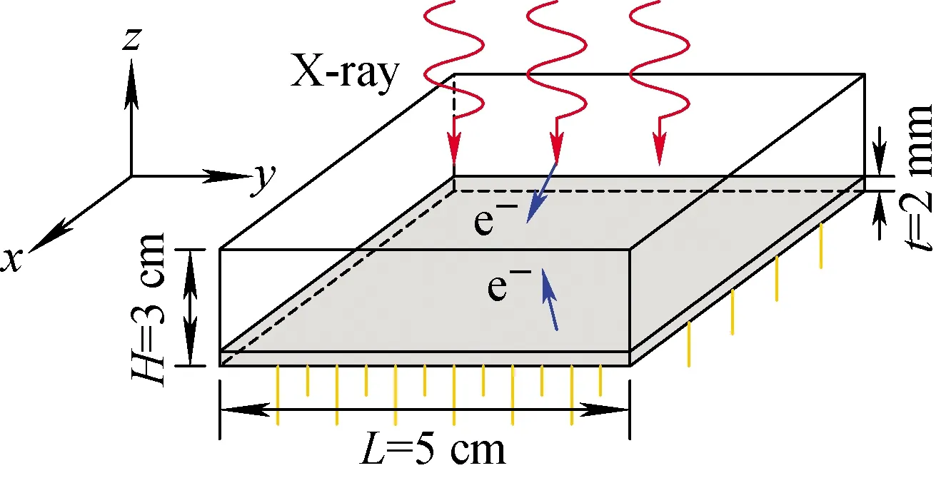
Fig.3 Computation model of shell and PCB of SIP

Table 1 Typical element of Kovar alloy
3.1 Photoelectron yield
The X-ray is assumed to illuminate the top of the shell vertically, and the energy is 50 keV, fluence is 0.01 J/cm2, and the half-width of duration is 1 ns. A Monte Carlo numerical simulation tool is applied to calculate the yields and energy spectra of photoelectrons.
The yield rates of photoelectrons emitting from Kovar alloy shell and PTFE are shown in Table 2. To simplify the simulation, we treat photoelectrons as mono-energetic electrons and consider the central energy instead of the spectra. Taking the X-ray fluenceφ, X-ray energyE, and area of the irradiated surfaceSinto account, the amount of X-ray photos is obtained and the total number of emitted electrons is calculated to beEe1=6.49×10¹⁰(emitting from Kovar alloy shell) andEe2=7.90×10⁸(emitting from PCB).

Table 2 Yield rate and central energy of photoelectron
3.2 Sampling point and sampling surface
Set the sampling points of electric field and magnetic field at the center of the dielectric plate 2 mm from the surface, where chips are most likely to be placed. The surface of the dielectric plate is applied as the sampling surface to obtain the number of deposited charges on circuits. The sampling point and sampling surface are shown in Fig.4.
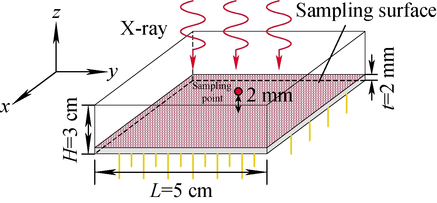
Fig.4 Sampling point and surface
3.3 EMI environment in shell of SIP
Considering the symmetry of geometry, the absolute value ofExandHxshould be equal toEyandHyrespectively. So, onlyEx,Ez,HxandHzof interest are shown in Fig.5.

Fig.5 Waveform of electromagnetic
The peak values of these waveforms indicate thatEzis in a more dominant position of the EMI environment. It could be more likely to induce interference current on the circuit lands or pins located along thezaxis.
The spatial distribution ofEzin the plane ofy=0 m at 1.5 ns is shown in Fig.6, which shows a change of the direction of polarization at the top and bottom of the shell. Considering that this EMI environment represents the characteristics of the photoelectrons, we could apply the static-field theory to explain these phenomena. Photoelectrons emitted into the shell could induce negative electric fields adjacent to the top of the shell, and induce positive electric fields adjacent to the surface of PCB. With the decrease of the distance from emission surfaces, the absolute values of electric fields become larger. The spatial distribution of photoelectrons at 1.5 ns is shown in Fig.7. In Fig.7, the red points represent the photoelectrons emitting from the top of Kovar alloy shell and the blue points represent the photoelectrons emitting from the surfaces of PCB.

Fig.6 Spatial distribution of Ez in plane of y=0 m at 1.5 ns
The frequency spectrum ofEzis shown in Fig.8. It is obvious that most of the energy is contained in the lower frequency under 2 GHz, and the frequency center is 33.33 MHz, which mostly depends on the characteristic time of X-ray like half-width of duration. On the other hand, we can observe a weak peak at 4.23 GHz, and this is the syntonic frequency of the shell. In other words, we should turn more attention to the low-frequency parts of the EMI environment, which contains most of the radiation energy.
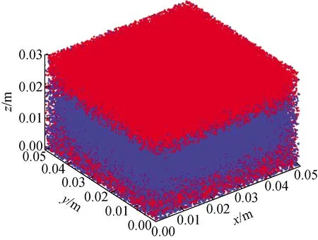
Fig.7 Spatial distribution of photoelectrons at 1.5 ns

Fig.8 Frequency spectrum of Ez
Moreover, we also investigate the deposited charges on dielectric plate. The amount of charge accesses the sampling surface within a pulse duration represents the deposited charges, and is shown in Fig.9. As shown in Fig.9, -1.84×10⁻⁹C of charges have deposited on dielectric plate, which is about 17.5% of total charges emitted into the shell. It’s not a low proportion, and may affect the system function.
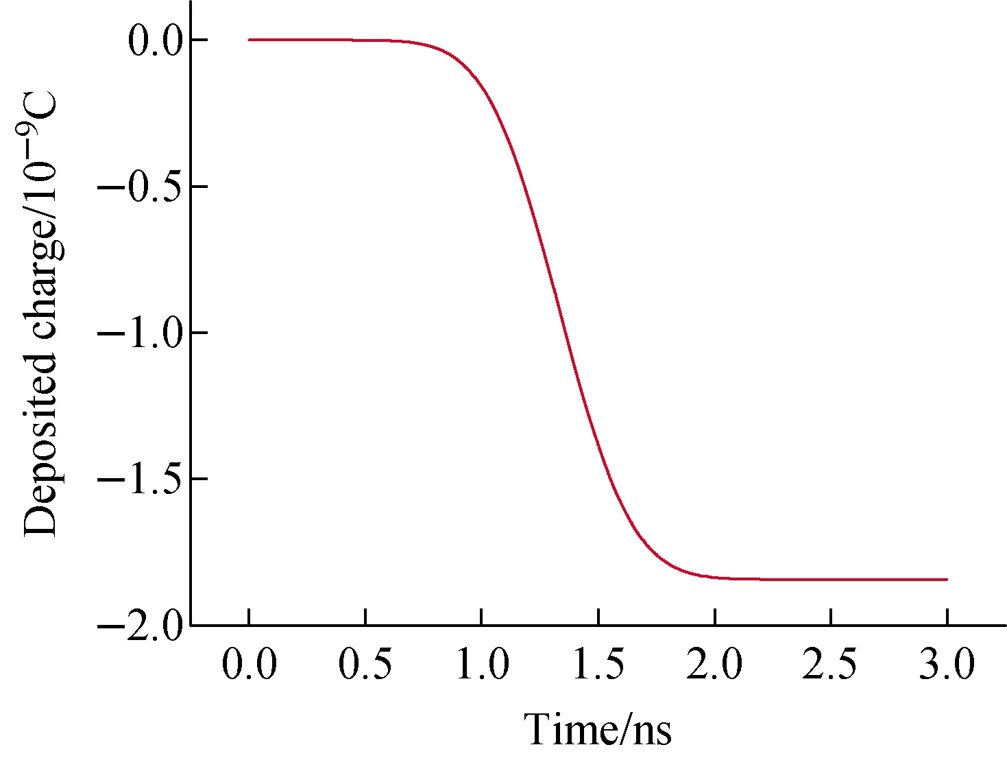
Fig.9 Deposited charge on dielectric plate
3.4 Influence of X-ray fluence

Fig.10 Change of electric field (Ez) versus fluence
Keep the time parameters of X-ray unchanged, the change of peak value ofEzversus fluence is shown in Fig.10. The electric field intensity increases linearly when the fluence is lower than 0.4 J/cm2, and when the fluence is higher than 0.4 J/cm2, the enhancement of space charge limited effect causes the emitting electrons form a barrier in front of the emission surface, which may discourage low-energy electrons from moving to the end of the shell, and for those that have enough energy to overcome the barrier, the space charge limited effect decreases their velocity[9-10]. This effect restricts the linear enhancement of electric field. Moreover, the deposited charge on the dielectric plate versus fluence is shown in Fig.11, and the nonlinear increase in charges also proves the influence of the space charge limited effect. The above results seem to indicate that there is an inherent upper limit on the EMI environment of SIP under X-ray radiation. When spectrum of X-ray is constant, the worst EMI environment only depends on the structure and material of SIP.

Fig.11 Change of deposited charge versus fluence
3.5 Influence of SIP size
By changing the irradiated area and height of SIP, the influence of size on EMI environment is studied. The parameters of X-ray are the same with the parameters in Section 3.1. Four areas are 3 cm×3 cm, 4 cm×4 cm, 5 cm×5 cm and 6 cm×6 cm with the same heightH=3 cm, and the four heights are 1 cm, 2 cm, 3 cm and 4 cm with the same area 5 cm×5 cm. Considering the intensity ofEzat the sampling point and the deposited charges on the dielectric plate, the change ofEzversus irradiated area is shown in Fig.12, and the change of deposited charges per unit area versus irradiated area is shown in Fig.13.
As is shown in Fig.12,Ezenhanced with the increase in area, however, there is an upper limitation of enhancement. For constant fluence of X-ray, the influence of area mainly bases on the elimination of electrons on the side walls of shell. The emission of electrons follows cosine distribution, thus some of the electrons will deposit on side walls before reaching PCB. The smaller the area, the larger the proportion of electrons deposited on side walls. On the contrary, larger area could weak the influence of side walls, which can be seen in Fig.13.
The change ofEzversus the height of SIP is shown in Fig.14, and the change of deposited charges per unit area versus the height of SIP is shown in Fig.15. With the increase in height, the intensity ofEzenhances first and then decreases. As is shown in Fig.6, there is a region of polarity change ofEz, and the region is in the middle of shell. If the sampling point is in this region, the intensity ofEzis low, that is why the deposited charge per unit area is the largest in Fig.15 for height 1 cm, but theEzis the lowest. However, the increase in height could reduce the number of electrons reaching PCB, and lead to the reduce ofEz.

Fig.12 Waveform of Ez of different irradiated areas of SIP

Fig.13 Deposited charge of different irradiated areas of SIP
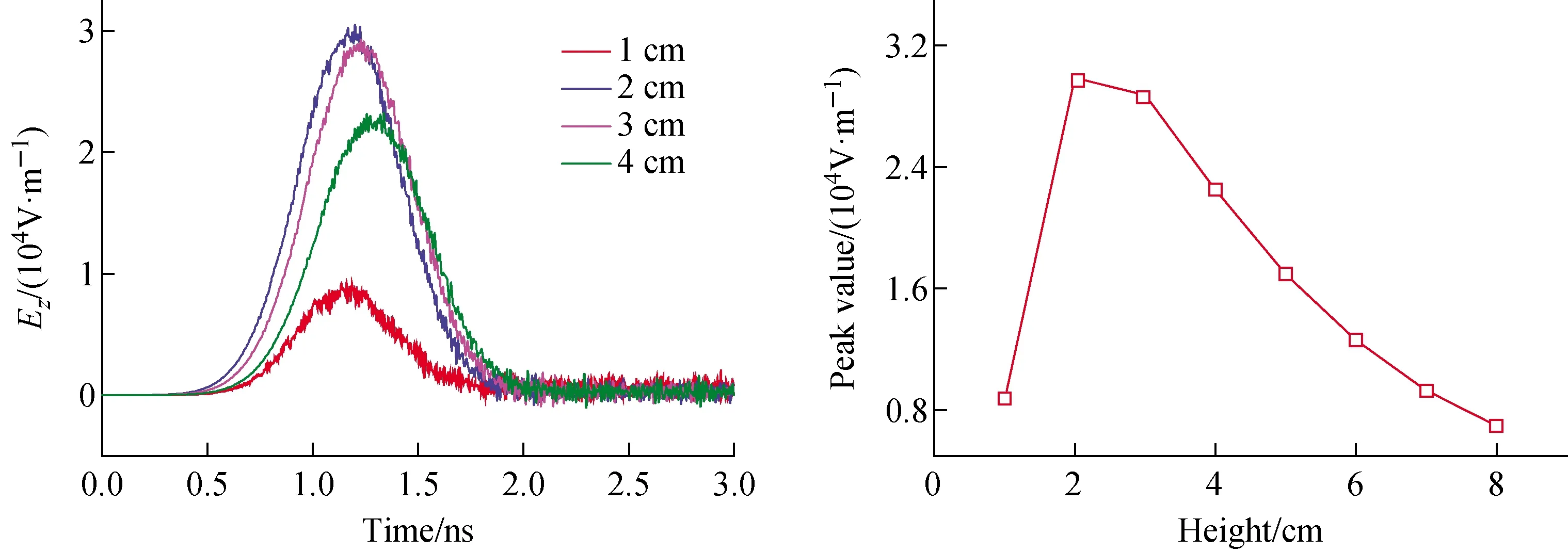
Fig.14 Waveform of Ez of different heights of SIP
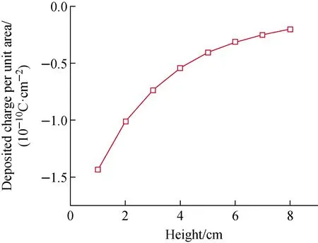
Fig.15 Deposited charge of different heights of SIP
4 Conclusion
The pulsed X-ray can induce EMI environment in the shell of a SIP. This EMI environment generated by the photoelectrons emitting from the Kovar alloy shell and PCB, could not be lessen by conventionally techniques. To evaluate the threat of this EMI environment, much attention should be paid to the region adjacent to the emission surfaces, where elements are more susceptible because of the larger electric fields. We should also focus importance on the low-frequency parts of EMI environment, which contain most of the radiation energy.
However, the threat degree of the EMI environment more likely depends on the structure and material of SIP. Reducing the size of the surfaces illuminated, and set the elements in the region of polarity change of electric field, or reducing the electron yield of shell, we could lessen the threat of EMI environment.
杂志排行
原子能科学技术的其它文章
- H-1NF仿星器标准磁场位形分析与高能量离子运动轨道模拟
- 铀转化生产线含氟废水处理工艺设计
- 在线进样ICP-MS用于239Pu气溶胶活度浓度连续监测技术研究
- Degradation Characteristic of Proton Irradiated 8T CMOS Image Sensor
- Comparative Experimental Study on Space Electrostatic Discharge Effect and Single Event Effect of 130 nm SOI D Flip-flop Chains
- Effects of Electron Irradiation at Different Energy and Fluences on Electrical Properties of InP HEMT Structure
