Degradation Characteristic of Proton Irradiated 8T CMOS Image Sensor
2021-12-15FUJingLIYudongFENGJieWENLinGUOQi
FU Jing, LI Yudong, FENG Jie, WEN Lin, GUO Qi
(1.Xinjiang Technical Institute of Physics and Chemistry, Urumqi 830011, China; 2.Xinjiang Key Laboratory of Electronic Information Material and Device, Urumqi 830011, China; 3.University of Chinese Academy of Sciences, Beijing 100049, China)
Abstract: The proton irradiation experiments with different energy were carried out on the new 8-transistor (8T) CMOS image sensors. As the total ionization dose (TID) effect and displacement damage dose (DDD) effect are caused simultaneously after proton irradiation, the degradation of device performance is more complicated. In order to specifically distinguish the main factor causing the degradation of different parameters, the equivalent TID method and equivalent DDD method were adopted. It is concluded that DDD mainly causes the degradation of dark current, while TID mainly causes the degradation of spectral responsivity, which has a guiding effect on the hardening design of image sensor in the irradiation environment.
Key words:CMOS image sensor; pinned photodiode; proton irradiation; total ionization dose; displacement damage dose
1 Introduction
With the progress of semiconductor technology, complementary metal oxide semiconductor (CMOS) image sensors are widely used in machine vision, 3D imaging, earth observation, as well as other space missions. Compared with traditional charge-coupled device (CCD), CMOS image sensor (CIS) has high integration and is easy to open multiple tracking windows simultaneously. In particular, the high resolution, pipelined global shutter mode, and the correlated double sampling (CDS) technology make the commercial 8-transistor (8T) CMOS pinned photodiode (PPD) image sensor gradually become the mainstream imaging device[1]. The global shutter mode ensures that all pixels are exposed simultaneously. Meanwhile, the CDS further reduces fixed pattern noise and dark noise[2]. As a result, 8T CIS can reduce pixel size while maintaining high performance and capture high-speed dynamic images without distortion.
However, when image sensor works in the irradiation environment, it is easily affected by the different particles, which leads to the degradation of electrical and optical parameters[3-4]. Important efforts have been made to understand the radiation effects on CISs in the past[5-8], but the use of 8T CISs has brought new behaviors that need to be studied in more detail. The degradation of device performance depends on the energy lost of the incident particle, which is mainly in two ways: The first is the total ionization dose (TID) effect, and the second is the displacement damage dose (DDD) effect. The ionization of particles in the device material produces electron-hole pairs, which then recombine, diffuse, and drift, eventually forming oxide trap charges or interface traps, then changing the parameter properties. High energy particles can cause lattice atoms to displace, resulting in pairs of interstitial-vacancy, and eventually form stable and metastable defects in the device.
After proton irradiation, total ionization damage and displacement damage occur at the same time. Degradation of 3T and 4T CIS pixels under proton irradiation has been reported[9-10]. Some of these studies suggest that the TID effect can be negligible under proton irradiation. Therefore, in this paper, the new 8T CIS was studied by proton irradiation with different energy, and the role of TID and DDD in parametric degradation was specifically analyzed.
2 Material and method
The tested chips are fabricated using 0.18 μm process technology and the detailed parameter is listed in Table 1. The pipelining allows exposure during read out, and the CDS reduces the fixed pattern noise and dark noise significantly.

Table 1 Electrical parameter of 8T CIS
CISs were exposed unbiased to 3 MeV, 10 MeV protons with fluence ranging from 3.68×10⁹to 9×1010cm-2at room temperature by the EN Tandem Van De Graaff Accelerator, Peking University. And the corresponding irradiation parameter is listed in Table 2.
The main parameter dark current and spectral responsivity were measured at pre- and post-irradiations. The dark current increases linearly with integration time before saturation. Therefore, under the condition of dark field, the dark current can be obtained by extracting the slope of the output signal with the integration time[11]. A spherical uniform light source is used to obtain the uniform light with a wavelength range of 450 to 800 nm. All parameters were tested within one week after irradiation[12]. At the same time, the degradation mechanisms of devices irradiated were analyzed by using equivalent displacement damage dose and equivalent total ionizing dose methods.

Table 2 Irradiation parameter
3 Result and discussion
3.1 Dark current and dark current distribution
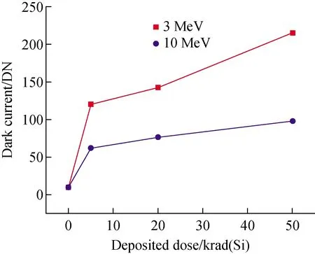
The thermal-generated charge caused by defects is called dark current. When the dark current is conjoined with the photogenerated carriers, and read as a signal, this will cause signal deviation.Fig.1 shows the degradation of dark current after 3 MeV and 10 MeV proton irradiation. It can be seen from Fig.1 that the dark current increases with the deposited dose. The situation after proton irradiation is more complex than that with gamma or neutron irradiation because it produces both TID and DDD effects. TID mainly leads to the accumulation of trapped positive charges in the dielectrics and the interface states. The density of these defects increases with TID, leading to the increase of dark current. DDD mainly generates SRH centers (point defects or defect clusters) in silicon bulk, and these defects act as the generating-recombination centers to generate bulk dark current. In conclusion, the dark current under proton irradiation of different energy increases with the deposited dose.

Fig.1 Variation of dark current with deposited dose for 8T CIS
TID threshold (44.6 krad(Si)) has been reported in60Co irradiation experiments[13]. When TID is lower than the TIDth, the dark current is almost constant. When TID is higher than the TIDth, the dark current increases with the TID. In this paper, the corresponding TID was calculated according to the proton energy and fluence used (Table 2), and it was found that the maximum equivalent dose did not reach the threshold value. It is preliminarily believed that the TID effect produced by 3 MeV and 10 MeV proton irradiation can be ignored for dark current. In order to verify this hypothesis, the distribution of dark current was further characterized, and the effect of TID and DDD on the dark current in 8T CIS was specifically analyzed by using equivalent DDD and equivalent TID methods.
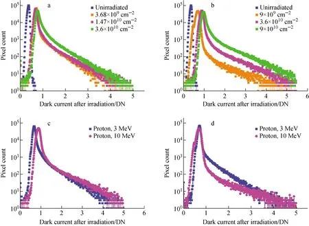
Through the statistics of the whole pixel array, the dark current distribution was obtained.Fig.2 shows the dark current distribution in the logarithmic scale after 3 MeV and 10 MeV proton irradiations. They both show a Gaussian distribution followed by an exponential hot pixel tail.
From Fig.2a and Fig.2b, the number of pixel presenting high dark current increases with fluence. This results in a serious decrease of the dynamic range. It is generally believed that the right shift of the Gaussian distribution is caused by TID. But the changes of the tail are caused by DDD. Similar conclusions have been reported in related literatures after high-energy proton and neutron irradiation[14-15].
The experimental results of the equivalent DDD and the equivalent TID methods are shown in Fig.2c and Fig.2d. According to Fig.2c, it is found that there is no significant difference in the degradation of dark current distribution of 8T CIS caused by 3 MeV and 10 MeV protons under the same DDD, and the whole curve is almost the same. According to Fig.2d, the Gaussian part is almost the same, while the 3 MeV’s tail is slightly larger than 10 MeV’s under the same TID. In other words, the number of pixels with high dark current produced by 3 MeV proton irradiation is more, and these pixels are mainly caused by bulk defects introduced by deposited DDD.
According to the equivalent TID and equivalent DDD methods, it is determined that displacement damage effect is the main cause of dark current degradation after 3 MeV and 10 MeV proton irradiations. TID damage has little effect on the dark current of the 8T CIS. Therefore, it can be inferred that the bulk defects are the main causes of the dark current degradation after proton irradiation.

a—3 MeV; b—10 MeV; c—Equivalent DDD; d—Equivalent TIDFig.2 Dark current distribution after proton irradiation
3.2 Spectral responsivity
In order to study the degradation of optical properties of 8T CIS after proton irradiation, the spectral responsivity under different energy and fluences was tested. The degradation of spectral response is reflected by the change of quantum efficiency at a certain wavelength. The quantum efficiency represents the device’s ability to convert photons into electrical signals. Generally, when photons are incident on the surface of the device, part of them are absorbed by the material to generate electron-hole pairs, forming a readout signal.
Fig.3a and Fig.3b show the decrease of quantum efficiency of 8T CIS prior and after proton irradiation at 3 MeV and 10 MeV. It can be seen that, for a certain energy, the quantum efficiency decreases seriously over all wavelength ranges with the increase of fluence. This is due to the fact that short-wave incident photons generate photo-generated carriers mainly at the surface. Therefore, under the influence of the oxide trap charges introduced by TID at the surface, the trap charges increase with the fluence, resulting in an increase in the surface recombination rate and a decrease in the surface carrier concentration[16-17], so the spectral response degrades in the short wave range. For long-wave incident photons, carriers are mainly generated in the depleted region. DDD mainly introduces displacement defects in the PPD depleted region, and the displacement defects serve as the recombination centers to capture the signal charges. Therefore, spectral response in the long wave range will also degrade[18-19]. Therefore, the spectral response decreases over the whole wavelength range after proton irradiation. In order to verify the main influencing factors of spectral response degradation after proton irradiation, we also adopted the equivalent TID and equivalent DDD methods.

Fig.3 Quantum efficiency variation of 8T CIS after 3 MeV proton irradiation (a), 10 MeV proton irradiation (b), equivalent DDD (3×10⁸ MeV·cm2/g) (c), and equivalent TID (50 krad(Si)) (d)
Fig.3c and Fig.3d show the degradation of quantum efficiency under equivalent DDD and equivalent TID respectively. Although the degradation of 3 MeV is more serious than that of 10 MeV proton irradiation, it can be seen that the quantum efficiency of the whole wavelength range decreases sharply under the same equivalent DDD condition, while the degradation is much smaller than that under the same equivalent TID condition. Therefore, it can be determined that the degradation of spectral response is mainly caused by TID, that is, with the increase of TID, the increase of surface interface state density leads to the increase of surface recombination rate, and the surface recombination rate dominates the degradation of spectral response.
According to the degradation of the spectral response after proton irradiation, we find that for proton irradiation, the quantum efficiency is severely reduced with the fluence. And TID damage has a great influence on the spectral responsivity of the 8T CIS.
4 Conclusion
In this paper, 3 MeV and 10 MeV proton irradiation experiments are carried out on the new 8T CMOS image sensors. The degradation of electrical and optical properties was studied after irradiation. Both the dark current and spectral responsivity are degraded seriously by proton irradiation. From the results of equivalent TID and equivalent DDD, the degradation of dark current is mainly affected by the DDD effects. The spectral responsivity is mainly affected by TID effects. That is, the increase of surface recombination rate leads to the degradation of quantum efficiency. The experimental results obtained in this paper are of great significance to further optimize the design of the image sensor and improve its radiation tolerance.
杂志排行
原子能科学技术的其它文章
- H-1NF仿星器标准磁场位形分析与高能量离子运动轨道模拟
- 铀转化生产线含氟废水处理工艺设计
- 在线进样ICP-MS用于239Pu气溶胶活度浓度连续监测技术研究
- Comparative Experimental Study on Space Electrostatic Discharge Effect and Single Event Effect of 130 nm SOI D Flip-flop Chains
- Effects of Electron Irradiation at Different Energy and Fluences on Electrical Properties of InP HEMT Structure
- 模拟二回路环境下乙醇胺与3-甲氧基丙胺复合水工况对304L不锈钢的缓蚀特性
