Threshold Voltage Model for DSOI MOSFET Considering Back-gate Current
2021-12-15WANGKeweiBUJianhuiHANZhengshengLIBoHUANGYangLUOJiajunZHAOFazhan
WANG Kewei, BU Jianhui, HAN Zhengsheng,*, LI Bo, HUANG Yang, LUO Jiajun, ZHAO Fazhan
(1.Institute of Microelectronics of Chinese Academy of Sciences, Beijing 100029, China; 2.Key Laboratory of Science and Technology on Silicon Device, Chinese Academy of Sciences, Beijing 100029, China; 3.University of Chinese Academy of Sciences, Beijing 100029, China)
Abstract: The relationship between the threshold voltage and the back-gate voltage of fully depleted DSOI NMOS is no longer satisfied with a single linear relationship after high total dose irradiation or high back-gate voltage. The coupling mechanism between the threshold voltage and the back-gate voltage will change after the back surface of the fully depleted DSOI device changes from the depletion region to the reversion region. Previous model is not enough to describe this phenomenon. In order to solve this problem, a new threshold voltage model was proposed considering the influence of back-gate current. The coupling relationship between the threshold voltage and back-gate voltage of the devices suffered from a high back-gate voltage or high total dose irradiation can be well fitted.
Key words:DSOI; FDSOI; total ionizing dose effect; threshold voltage; back-gate voltage
1 Introduction
SOI (silicon on insulator) devices are widely used in modern high-speed and low-power circuits and the aerospace industry. Compared with the traditional bulk silicon devices[1], SOI devices have an extra SiO2layer called BOX (buried oxide) to isolate the transistor from the substrate. All transistors are built on this insulator layer, which makes the transistors independent from each other. This structure makes the SOI circuit completely eliminate the parasitic latch effect, and it has the advantages of suppressing the short channel effect and high integrated density[2-5]. For fully depleted SOI (FDSOI) devices, due to the depletion of all the body regions when the transistor is turned on, the electric field between the two surfaces of the silicon film will couple with each other. It means that the change of the surface potential of the back surface will influence the threshold voltage of the front channel. This coupling relationship has been derived in detail in the paper of Lim et al[6]. Therefore, the threshold voltage (Vth) of FDSOI devices can be adjusted by applying a back-gate voltage to the substrate, which makes the application of FDSOI devices more flexible.
Due to the existence of the BOX layer, SOI devices are sensitive to total dose irradiation. Charge traps will be generated in the SiO2under radiation environment, most of which are hole traps. The positive potential generated by the hole traps in the BOX will play a role like the back-gate voltage. The accumulation of positive charges will make the threshold voltage of n-type devices degenerate continuously[7-9]. To solve this problem, a negative voltage can be applied to the back-gate to artificially eliminate the degradation of the threshold voltage by radiation and extend the life of the devices[10-12]. In order to apply appropriate back-gate voltage to devices with different degradation degrees, it is necessary to model the relationship between threshold voltage and back-gate voltage under different irradiation doses.
It is observed that the relationship between threshold voltage and back-gate voltage deviates from the theoretical coupling relationship in the depletion region when the device is suffered from a high dose of irradiation. This is because when the positive charge accumulated in the BOX is large enough, the channel of back-gate will be turned on and the back-gate current will be formed at the back-channel. When the back surface has transformed to the inversion state, the mechanism of the threshold voltage changing with the back-gate voltage is no longer the same as that of the depletion state.
A model of the relationship between threshold voltage and back-gate voltage when the back-channel of the DSOI device is turned on is proposed in this paper by analyzing the working principle of DSOI device under high total dose irradiation and different back-gate bias conditions. By extracting a parameter from the test data measured from normal devices, the data measured from devices suffered from total dose irradiation can be well fitted.
2 Experiment detail
Double SOI (DSOI) devices were used in our experiments. The structure of DSOI device is shown in Fig.1, and the device parameters are listed in Table 1. According to the depletion state of the top silicon film, the DSOI device used here belongs to the FDSOI. Compared with conventional SOI devices, DSOI devices have an extra silicon layer in the box, which can be used as an independent electrode to apply the back-gate voltage to a single transistor. In addition, because there is no limitation from the PN junction in the substrate, the back-gate voltage can be adjusted in a wider range.
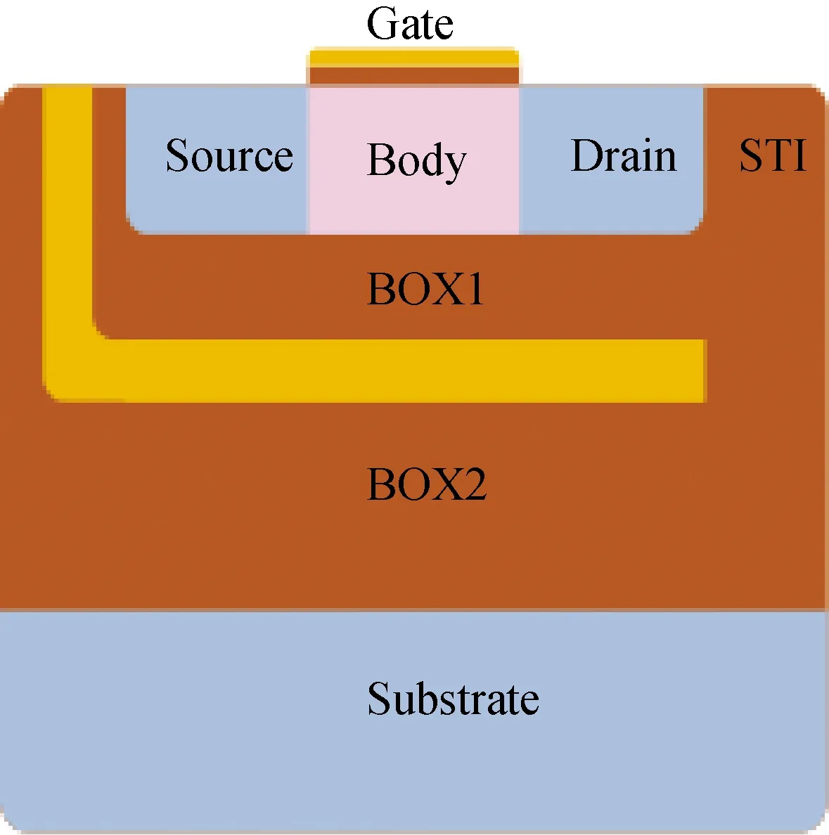
Fig.1 Structure of DSOI MOSFET

Table 1 Technology parameter for FD DSOI nMOSFET
The DSOI nMOSFETs were irradiated with60Co γ-ray at a dose rate of 50 rad(Si)/s. The OFF-bias condition was used in this experiment, the drain was biased at 1.8 V, source and gate were grounded. To avoid the annealing effect, electrical measurements were performed in 2 hours after each irradiation dose at 0.1, 0.3, 0.5, and 1 Mrad(Si), respectively. TheIds-Vgscharacteristics were measured withVdsat 0.1 V by Agilent B1500A semiconductor parameter analyzer at room temperature. Four different back-gate biases of 0, -1, -3 and -5 V were used in the measurement.
All threshold voltages are extracted by GM method.
3 Result and analysis
The measured results ofVth-Vbgare illustrated in Fig.2 with the dose from 0 rad to 1 Mrad and the back-gate voltage from 0 V to -5 V. It can be easily found that the higher irradiation dose is, the faster the threshold voltage changes with the back-gate voltage. This phenomenon shows that the relationship between back-gate voltage and the threshold voltage of the device is not a simple linear one at least after a high dose of irradiation.
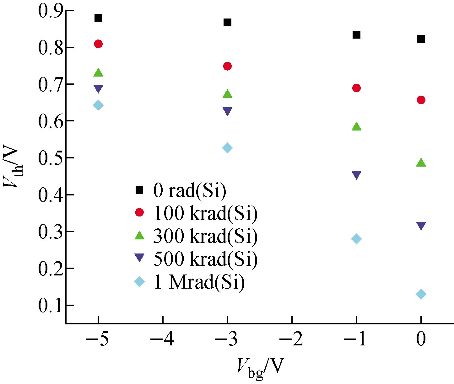
Fig.2 Vth-Vbg curves with different total irradiation doses
In the work of Lim et al.[6], we can get the formulas (1) and (2) which were used to describe the coupling relationship of the back-gate voltage (Vbg) and the threshold voltage of the front-gate (Vthf).
(1)
(2)
When the device is suffered from a high dose of irradiation, the accumulated holes in the BOX layer may cause the back surface to reach the inversion state and turn on the back-channel. Theoretically, when the back surface is in the inversion state, the back-gate voltage will no longer affect the threshold voltage of the front-gate due to the shielding effect of the charges in the inversion layer. However, the back-gate current is formed after the back-gate is turned on, which will still increase with the increase of the back-gate voltage, and then be collected at the drain. As a result, when the back-gate is turned on, the measuredIds-Vgscurve will drift with the increase of the back-gate voltage, whereIdsis the drain current andVgsis the gate voltage, and then the extracted threshold voltage will continue to change.
4 Model building
Because the influence of the positive charge generated by radiation in the BOX layer can be equivalent to the influence caused by a certain positive back-gate voltage, it is of great significance to study how the characteristics of DSOI devices change with the back-gate voltage under normal non-irradiated conditions. TheIds-Vgscurves measured by the DSOI device under normal conditions with the back-gate bias changing from 1 V to 15 V is shown in Fig.3. The actual measured back-gate voltage range is -15-15 V, which is not completely shown in Fig.3 because of the small variation of the curve under negative back-gate bias. The threshold voltage of the device under different back-gate bias conditions from -15 V to 15 V is shown in Fig.4.

Fig.3 Ids-Vgs curve from Vbg =1-15 V
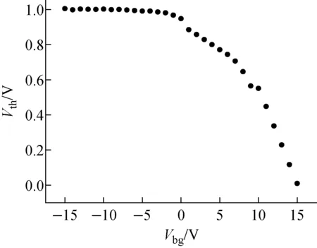
Fig.4 Measured result of Vth-Vbg curve with Vbg changing from -15 V to 15 V in normal situation
It can be seen from Fig.3 that when the back-gate voltage is small, the interval of the curve is small. When the back-gate voltage increases, the interval between curves also increases. In Fig.4, theVbg-Vthcurve can be divided into three linear regions. The first one, from -15 V to 1 V, is almost a flat line, this is because screening effect of the charges accumulated at back surface when the negative back-gate voltage is applied. The second one is from 1 V to 8 V, corresponding to the depletion state of the back surface. In this region, formula (1) and (2) can be used to describe the coupling relationship. In fact, the range of the depletion region can be calculated by using the real device parameters which is from 1.11 V to 7.87 V. The theoretical calculation results are very close to the test results. The third linear region is from 8 V to 15 V, corresponding to the inversion state of the back surface. The threshold voltage of the device is still changing because of the increase of the back-gate current.
When the back-gate is turned on, the shift distance of theIds-Vgscurve is proportional to the increment of the back-gate current.
Formula (3) and (4) are currents of the front and back channel when they are turned on respectively.
(3)
(4)
WhereWandLare the width and length of both channels respectively;μfandμbare the electron mobilities of the front and back channel respectively;Vgis the voltage applied to the front-gate;Vthbis the threshold voltage of the back-gate.
In order to simplify the calculation,μbis assumed to be a constant and will not change with the back-gate voltage. From formula (4), when the back-gate voltage increases by 1, the increment of the back-gate current is formula (5).
(5)
It means, when the back-gate voltage increases by 1, theIds-Vgscurve will move up by ΔIdsb. The lateral shift distance of theIds-Vgscan be achieved by using the maximum tangent of theIds-Vgscurve which isk0in formula (6).
(6)
Whereμfgmis the mobility of the front-gate when the transconductance curve reaches the maximum, which can also be viewed as the maximum mobility of the front-gate when the front gate voltage is scanned from -1 V to 2 V.
Now, the new coupling relationship in the inversion region can be calculated which iskIin formula (7).
(7)
WhereMrepresents the ratio ofμbandμfgm.Mis a parameter that needs to be extracted, because in practice, mobility is changing with bias conditions, and it is closely related to the level of the device manufacturing process. So, it is difficult to accurately predict the value ofMof different batches or process levels. However, it has been proved by research that the mobility of the back-channel is larger than that of the front-channel for FDSOI devices as a whole. Predictably,Mshould be greater than 1[13-15].
From the above derivation, the relationship between the threshold voltage and the back-gate voltage after the back-gate has been turned on is:
(8)
5 Model verification
The simulation results and measured data from normal devices without any radiation are shown in Fig.5. Where the region from -15 V to -1.11 V is fitted with a flat line. The region from -1.11 V to 7.87 V is fitted with the coupling relationship in the depletion region. The last region from 7.87 V to 15 V is fitted with formula (8).Mis extracted to be 3.4 which is consistent with the prediction. The data measured after TID experiments can be fitted with the same model with the sameMand the results are shown in Fig.5.
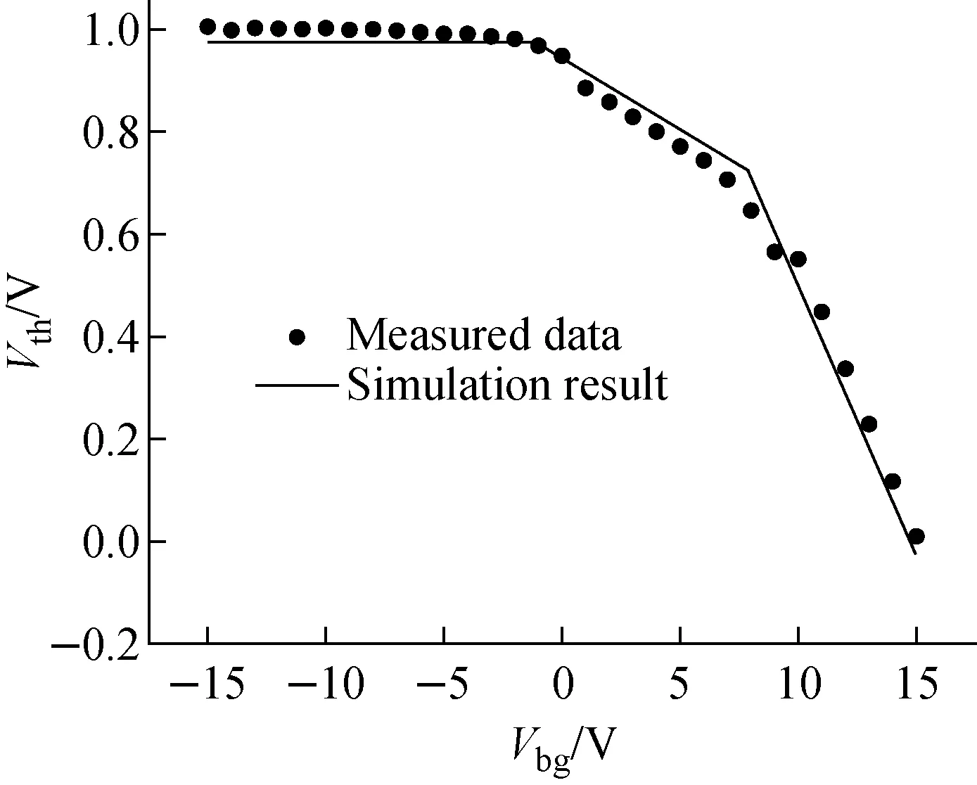
Fig.5 Simulation result and measured data in normal condition
The shift of the simulation lines was only controlled by the concentration of the positive charges trapped in the BOX which is changing with the dose of irradiation and can be fitted with logarithmic function[16]. The charges of the surface states were ignored here because of their small amount compared to the number of charges in the thick BOX. Simulation results and measured data for threshold voltage of device with total dose irradiation are shown in Fig.6. As shown in Fig.6, the simulation results match well with the measured data.
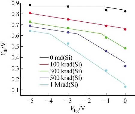
Fig.6 Simulation results (lines) and measured data (dots) for threshold voltage of device with total dose irradiation
6 Conclusion
A model to describe the relationship between the threshold voltage and the back-gate voltage of DSOI device after the back-gate is turned on is proposed in this paper. The model can be used to fit the relationship between the threshold voltage and the back-gate voltage of DSOI device under the total dose irradiation by extracting one parameter from normal devices. The model fits the measured data well.
杂志排行
原子能科学技术的其它文章
- H-1NF仿星器标准磁场位形分析与高能量离子运动轨道模拟
- 铀转化生产线含氟废水处理工艺设计
- 在线进样ICP-MS用于239Pu气溶胶活度浓度连续监测技术研究
- Degradation Characteristic of Proton Irradiated 8T CMOS Image Sensor
- Comparative Experimental Study on Space Electrostatic Discharge Effect and Single Event Effect of 130 nm SOI D Flip-flop Chains
- Effects of Electron Irradiation at Different Energy and Fluences on Electrical Properties of InP HEMT Structure
