Characterization of Single Event Transient in 14 nm FinFET Technology
2021-12-15WANGBinSHIZhuYUEHongjuLIHaisongLUHongliYANGBo
WANG Bin, SHI Zhu, YUE Hongju, LI Haisong, LU Hongli, YANG Bo
(Xi’an Microelectronics Technology Institute, Xi’an 710065, China)
Abstract: In order to evaluate the intrinsic radiation hardness of the fin field effect transistor (FinFET) device, the characteristics of single event transient (SET) were studied by 3D technology computer-aided design (TCAD) simulations in the 14 nm FinFET technology. The results show that the single-event sensitivity varies according to LET values and incident positions. The width of SET pulse broadens with the increase of LET values. Besides, the response of SET has a complicated relationship with the strike location. For low-LET values (LET≤1 MeV·cm2/mg), the SET response has a strong dependency on the place where it is struck by heavy ions. For high-LET values (LET>10 MeV·cm2/mg), the strike location dependency of the SET response diminishes due to the enhanced substrate charge collection.
Key words:single event transient; FinFET; heavy ion; LET; TCAD
1 Introduction
With the scaling of the feature size of integrated circuits (ICs), short-channel effects (SCEs) limit the application of planar technologies. To solve this problem, fin field-effect transistor (FinFET) was proposed by professor Hu[1], firstly. Consequently, the power supply voltage and the node capacitance also diminish, which leads to more and more serious soft errors caused by ion exposure[2-5]. As the feature size of device is reduced to 14 nm and below, the proportion of SET increases significantly[6], which is one of the key factors affecting the reliability of nano FinFET devices.
International scholars have researched the SET response of bulk FinFET and conventional planar devices in both simulation and experiment extensively. Fang et al.[7]simulated charge collection of bulk FinFET and planar devices under neutron irradiation. The results show that FinFET devices exhibit a lower soft error rate than planar devices, since the charge collection and the diffusion of substrate charge are reduced by the drain region of FinFET devices decreasing. Hubert et al.[8]studied the effects of technology scaling on soft error rate in the planar and FinFET technology. The results demonstrate that FinFET technology exhibits better single-event (SE) performance than planar counterpart due to the smaller sensitive region of the device. Nsengiyumva et al.[9]compared the SET pulse widths between 16 nm bulk FinFET and 28/20 nm planar device using technology computer aided design (TCAD) simulation tool. It is found that a SET pulse width reduction as high as 50% is achieved in comparison with the planar technology. Harrington et al.[10]investigated the correlation of SET characteristics of 14/16 nm bulk FinFET technology with device threshold voltage change and the number of transistor fins by heavy ion radiation. The results illustrate that transistor drive current plays an important role to the SET cross-section at high LET values and determines the SET pulse width. In addition, heavy ion experiments were carried out to compare the SEU trends of DFF in the 16 nm bulk FinFET technology and 28/20 nm bulk planar technology by Patrick et al[9]. The experimental results show that SEU cross-section of a DFF in the 16 nm FinFET technology has several orders of magnitude lower cross-section than that of 28/20 nm planar technology when LET is less than 10 MeV·cm2/mg. However, for higher LET values, the SEU cross-section decrease isn’t observed with the shrinking of size. In conclusion, the SET characteristics of FinFET devices have a complex relation with heavy ion and incident positions[11-14].
In this paper, the sensitivity of SET with different LET values and incident locations will be studied by using three-dimensional (3D) TCAD simulation tools in the 14 nm FinFET technology. The results can provide a good complement to the SET characteristics of the FinFET technology, as well as give a theoretical guidance for the radiation hardening strategy of 14 nm FinFET devices.
2 Device under test and experimental setup
3D TCAD modeling and simulations of devices are useful in providing insight into physical mechanisms and failure models due to single-event effects. In this work, 3D TCAD simulations are utilized to investigate charge collection mechanisms and SET pulse widths in the 14 nm FinFET technology.
2.1 3D device design and calibration
The physical device of two-fin n-channel FinFET (nFinFET) is designed by Sentaurus TCAD in the 14 nm technology node, as shown in Fig.1. The design parameters of the simulated device are listed in Table 1. The electrical characteristic curves of the nFinFET are calibrated against theI-Vdata from commercial process design kits (PDKs), and the calibration results are shown in Fig.2.
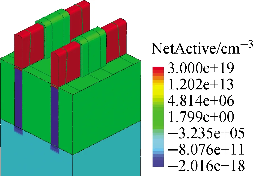
Fig.1 Structure of 14 nm NMOS FinFET designed by TCAD

Table 1 Design parameter for 14 nm nFinFET device

a—Transconductance characteristic curve; b—Output characteristic curveFig.2 Electrical characteristic curve of nFinFET
2.2 3D TCAD simulation setup

Fig.3 Schematic diagram of TCAD mixed simulation
A mixed-mode is conducted to study the radiation effect of an inverter in the 14 nm FinFET technology. The diagram of the mixed simulation is shown in Fig.3. In the inverter, p-channel FinFET (pFinFET) uses the BSIM-CMG model which comes from the PDKs, and the nFinFET uses the physical devices. The nFinFET and pFinFET devices each consist of two fins and one single gate finger (NFIN=2 and NF=1). These nFinFET and pFinFET transistors are designed as minimum size transistors according to the design rules of the 14 nm bulk FinFET technology. The gate length of PMOS (Lg) is set to 16 nm, and the load capacitance (CL) is equal to 0.1 fF. The supply voltage of the inverter is set to 0.8 V.
In the selection of physical models, the following models are used: 1) Fermi-Dirac statistic, 2) bandgap narrowing effect, 3) con-centration dependent Shockley-Reed-Hall and Auger recombination model, 4) considering the effects of temperature, doping, electric field and carrier scattering on carrier mobility, 5) the carrier transport equation is based on the hydrodynamic model, 6) heavy ion model with Gaussian distribution, a characteristic coefficient of 1/e, a radius of 10 nm. Unless specifically defined, other models or parameters use the default parameters of the Sentaurus TCAD software.
The position of heavy ion strike is set to the single-fin drain center (SFDC) and the double-fins space center(DFSC) at normal incident and room temperature, as shown in Fig.4. For all of these simulations, the particle LET is changed from as low as 0.1 MeV·cm2/mg to 40 MeV·cm2/mg.
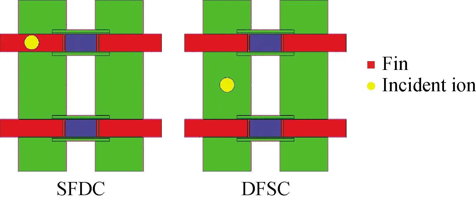
Fig.4 Diagram of location of FinFET device struck by heavy ion
3 3D TCAD simulation results
To investigate charge collection mechanisms and SET pulse width trends for the 14 nm bulk FinFET, 3D TCAD simulations are conducted. The results of simulation are shown in Fig.5, which depicts the inverter output as a function of simulation time at different LET values and incident positions. During the simulation, the input of the inverter is biased to a low level (Vin=0 V), and normally the output is high (Vout=0.8 V). The simulation time is set to 500 ps. The specific locations (SFDC and DFSC) of nFinFET are hit by heavy ions at 100 ps. The SET pulse width is defined as the width corresponding to the half of supply voltage (VDD/2). The results are listed in Table 2.
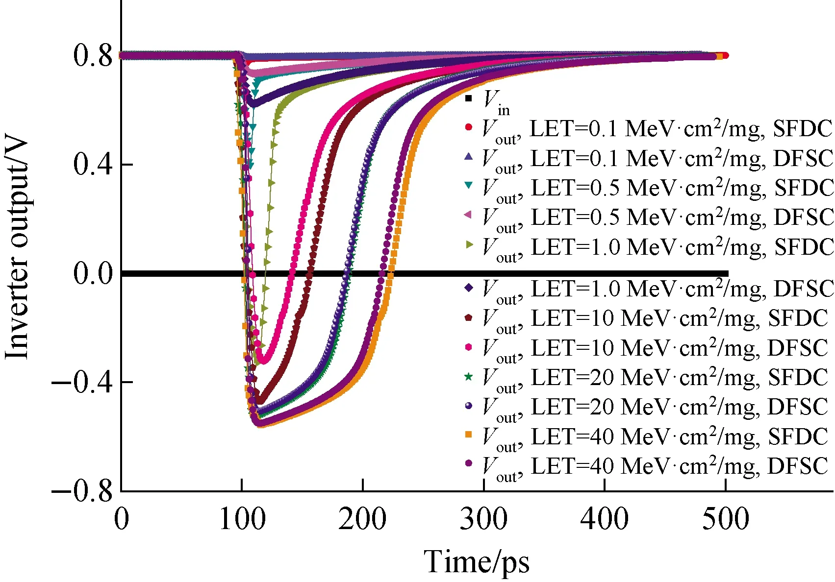
Fig.5 Output of 14 nm FinFET inverter with different LET values and different incident positions
The simulation results in Table 2 show that the SET pulse width broadens with the increase of LET values. There is no SEU observed in the inverter when LET<0.5 MeV·cm2/mg. The LET threshold of SFDC struck by heavy ion are 0.5 MeV·cm2/mg, while the LET threshold of DFSC is greater than 1 MeV·cm2/mg. The SET pulse width as a function of LET value is shown in Fig.6.
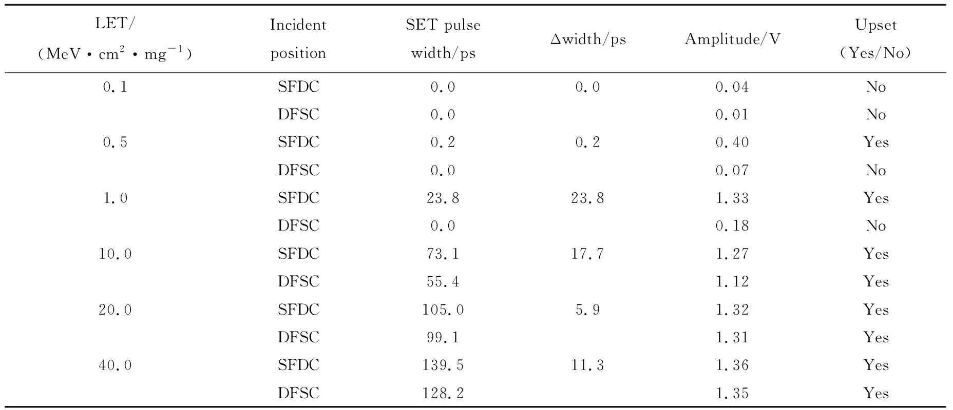
Table 2 SET pulse width at different LET and incidence positions
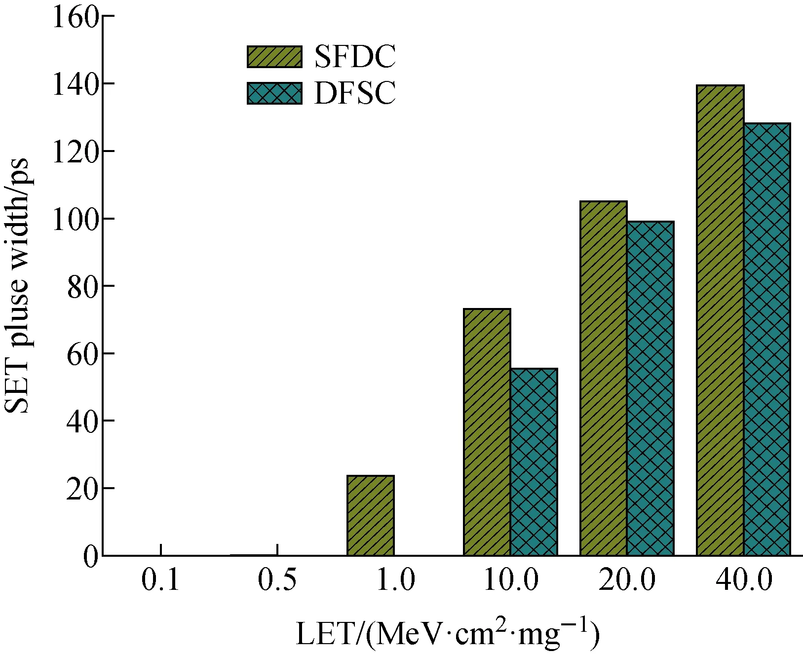
Fig.6 SET pulse width as a function of LET value
In addition, when the LET is less than 1 MeV·cm2/mg, the pulse current of the SET is similar to a double exponential current source. However when the LET is greater than 10 MeV·cm2/mg, the pulse current of the SET has a unique platform region as shown in Fig.7. The platform width determines the voltage pulse width of the SET.
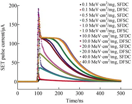
Fig.7 SET pulse current as a function of simulation time
4 Analysis and discussion
4.1 Effect of characteristic radius of ion track structure on SET pulse width
In the modern CMOS circuits, characteristic gate length of devices are now less than 20 nm, and the response time of circuit-switching is below 10 ps. Therefore, it is very important to choose the spatial and temporal distribution when simulating the device and circuit SET using 3D TCAD. As shown in Fig.8, the influence of characteristic radius on the SET pulse width is studied by using 3D TCAD simulation. The results show that the SET pulse width increases with the decrease of ion track radius in the 14 nm bulk FinFET inverter when the LET is equal to 1 MeV·cm2/mg. However, the SET pulse width is similar regardless of the characteristic radius when the LET increases to 40 MeV·cm2/mg, due to the enhanced FinFET substrate charge collection. These results are also consistent with the simulated FinFET SE response trends reported in reference [15]. The article points out that the simulation results are in good agreement with the experimental results when the radius of ion track is set to 10 nm in the 14 nm bulk FinFET technology. Therefore, the characteristic radius of ion track is set to 10 nm in this study. In the other technology the value of characteristic radius must be chosen carefully, especially for low LET particles.
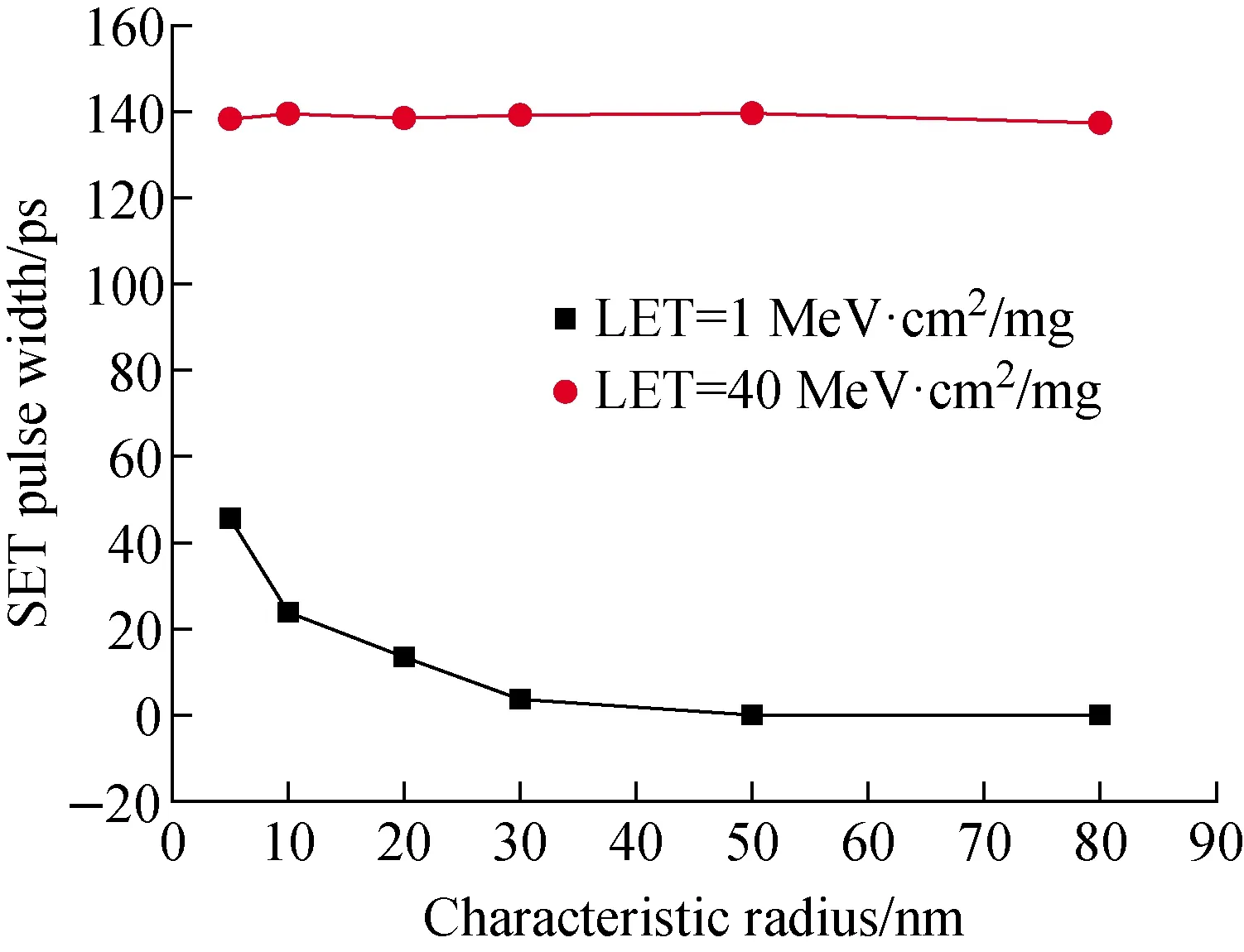
Fig.8 SET pulse width as a function of characteristic radius of ion
4.2 Effect of angular effect on single-event mechanism
It is well known that the total charge collection increase with the increase of the incident angle in the planar bulk technology, because the length of charge collection is longer than normal incident. This is equivalent to increase the effective LET value. For a FinFET technology, angular effects have an important influence on SE mechanisms due to the discrete structure of FinFET device[16-17]. The results of researchers show that angular upset cross sectional characteristics can be attributed to different charge deposition regions in the fin and the subfin bulk structures[17]. Zhang et al.[16]have studied angular effects of heavy-ion strikes on single-event upset response of flip-flop designs in 16 nm bulk FinFET technology. The results show that upset probability and SEU cross-sections increase with tilt angles, but those decrease with the increase of roll angles for low-LET heavy-ion incidence. The main reason for this behavior is posited to be variations in charge track length within active Si regions.
4.3 Effect of LET value on characteristic of SET
The simulated SET pulse widths for the 14 nm bulk FinFET technology increase with LET value, as shown in Fig.6. As we all know, if the LET value is higher, the ionization capability is stronger, generating higher concentration electron-hole pairs. Then enough charge is collected by the sensitive nodes of the device and the wider SET pulse is obtained. Charge collection mainly consists of two processes that are drift under the electric field of drain and diffusion forced by concentration gradient, respectively. At low-LET values, the drift process plays an important role in charge collection, sustaining the tens of picoseconds after heavy ion incidence. At high-LET values, the diffusion process will dominate the charge collection after drift process, and form the current platform which determines the width of SET pulse. The SE response behavior of FinFET circuits at high-LET values is attributed to the increased charge collection from the substrate.
4.4 Effect of incident position on characteristic of SET
The physical mechanisms of charge collection varies according to the incident positions. When the SFDC is struck directly by heavy ion, charges are collected through drift and diffusion, as shown in Fig.9a. When the DFSC is struck, charges are collected through diffusion, as shown in Fig.9b. As a result, the SET response of the 14 nm bulk FinFET inverter has a strong dependency on the ion strike location for low-LET particle strike (LET≤1 MeV·cm2/mg). Results show that a direct ion striking at the fin generates an observable SE transient while an ion striking between two fins results in a very small voltage perturbation at LET=1 MeV·cm2/mg. For struck by particles with high-LET values, the strike location dependency of FinFET SE response diminishes due to the enhanced substrate (diffusion) charge collection.
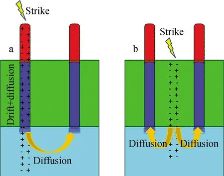
a—Collected through drift and diffusion; b—Collected through diffusion Fig.9 Charge collection at different incident locations
5 Conclusion
In this paper, 3D TCAD simulations of the struck inverter are used to explore charge collection mechanisms and SET pulse widths as a function of particle LET values and incident positions in 14 nm bulk FinFET technology. The results show that the SET pulse width increases with the LET value. For low-LET values (LET≤1 MeV·cm2/mg), the SET response of the 14 nm bulk FinFET inverter has a strong dependency on the ion strike location. For high-LET values (LET>10 MeV·cm2/mg), the SET response dependency on the strike location diminishes due to the enhanced substrate (diffusion) charge collection.
杂志排行
原子能科学技术的其它文章
- H-1NF仿星器标准磁场位形分析与高能量离子运动轨道模拟
- 铀转化生产线含氟废水处理工艺设计
- 在线进样ICP-MS用于239Pu气溶胶活度浓度连续监测技术研究
- Degradation Characteristic of Proton Irradiated 8T CMOS Image Sensor
- Comparative Experimental Study on Space Electrostatic Discharge Effect and Single Event Effect of 130 nm SOI D Flip-flop Chains
- Effects of Electron Irradiation at Different Energy and Fluences on Electrical Properties of InP HEMT Structure
