Research on Single Event Transient Effect Protection of Switching Power Supply for Satellite Payload
2021-12-15YANGXiaobinLUODanMAKuianZHUHaiLIUYongfeng
YANG Xiaobin, LUO Dan, MA Kuian, ZHU Hai, LIU Yongfeng
(Xi’an Institute of Space Electronic Information Technology, Xi’an 710100, China)
Abstract: The generation process, propagation mechanism and the impact on the switching power supply of the single event transient effect in the PWM (pulse width modulator) are analyzed in this paper. Combined with the technical characteristics of the satellite payload’s dedicated power supply, an effective protection strategy is proposed. The correctness of the mechanism analysis and the effectiveness of the improvement measures is verified by the pulsed laser and heavy ion test methods. It provides new ideas for eliminating the major hidden dangers of such devices in space applications.
Key words:satellite payload; switching power supply; single event transient effect; pulse width modulator; protection strategy
1 Introduction
A large number of electronic devices on space vehicles (artificial satellites, manned spacecraft, etc.) require special switching power supplies to supply power. The stability of its power supply is directly related to the reliability and safety of the aircraft in orbit.
Different from the ground environment, the satellite payload switching power supply operating in the space environment is very susceptible to the influence of the radiation environment. There are two main effects: total dose effect and single event effect.
For the total dose, the current research is systematic and in-depth, and its shielding and reinforcement measures are proved to be effective. Moreover, because the total dose is a cumulative effect, even if there is a deviation in the design margin, the damage often occurs at the end of the life of the product in orbit and the impact is relatively limited.
At the same time, the impact of single event effects on satellite electronic equipment is becoming more and more prominent, but the current research on it is not deep enough, especially for single event transient (SET) effects. SET often acts on the pulse width modulator (PWM), which is the core control chip of the switching power supply. SET causes the output voltage of the switching power supply to drop instantaneously, and even causes the device in orbit to shut down abnormally, which brings great challenges to the stable operation of the satellite in orbit. However, a lot of research work still focuses on the measurement method of SET effect currently, and how to take protective measures effectively is not fully studied[1-7].
2 Analysis of single event transient effect of PWM
Related studies show that the impact of single event effects on analog devices is mainly manifested as SET[6], which is a single high-energy particle acting on the sensitive area of a semiconductor device, resulting in instantaneous changes of voltage and current of device. SET will cause abnormal operation of analog linear circuits, such as clock, operational amplifier and IO. This abnormal signal can easily propagate along the combinatorial logic like a normal signal, and is caught by the latch at the end to form a persistent error. Such error usually does not cause complete damage to the PWM[8], but narrows the duty cycle of the output drive signal[9].
UC1825A is the product of American TI Company. Its circuit function block diagram is shown in Fig.1. In order to realize the power-on soft start function, an external capacitor is connected to the ground at the soft start terminal of the chip.
It can be seen from Fig.1 that UC1825A contains three latches: PWM latch (latch 1), Fault latch (latch 2), and Restart delay latch (latch 3).
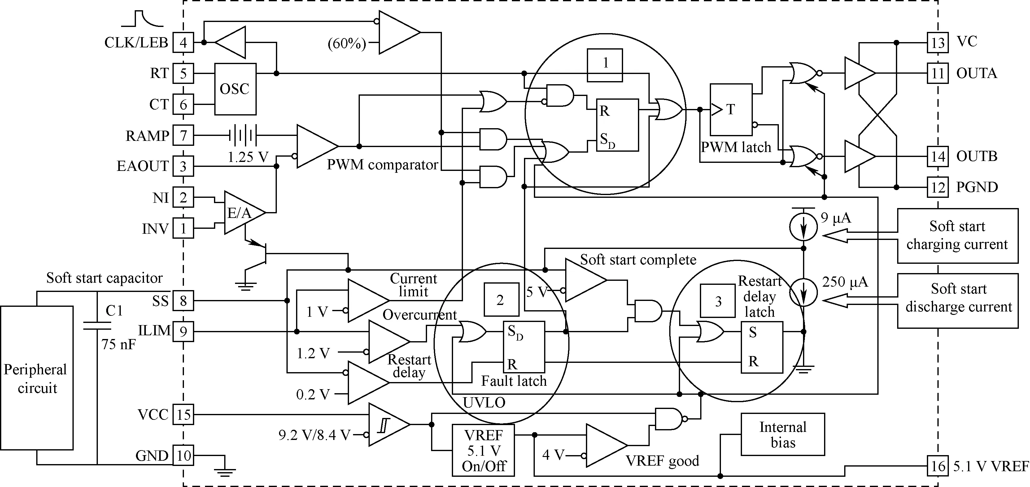
Fig.1 Block diagram of chip principle and schematic diagram of soft start capacitor
The later two latches have no continuous reset signal. When encountering a single event bombardment, the instantaneous glitch signal is easily captured by the latch 2 or latch 3 at the end, forming a persistent error, and resulting in the continuous loss of pulse width output.
Through analysis, the mechanism of the loss of the sustained pulse in UC1825A is as follows. When the switching power supply PWM encounters a single event, firstly it induces instantaneous changes of the voltage and current of the analog circuit inside the chip (such as the operational amplifier and its peripheral circuits), which causes the output of the latch 2 to become high. The high level is transmitted backward along the two branches respectively, and finally has two completely different effects on the PWM operation.
1) The high level is transferred to the upper part of Fig.2. First, after passing through an OR gate, the output of the OR gate becomes 1, the output of the PWM latch setting becomes 1, and the output of the subsequent OR gate becomes high. The output of the subsequent NOR gate becomes 0, and the final drive output signal becomes 0. At this time, the power MOSFET of the switching power supply has no driving signal, and the output voltage of the power supply drops. If the logic keeps changing subsequently, the output voltage will continue to drop, and after a period oft1, it will completely shut down. The relevant logic state is shown in Fig.2.
2) The high level is transmitted to the right in Fig.2. After passing the AND gate, the output becomes 1 (because the soft start terminal voltage of PWM is 5.2 V, the comparator output is high, and the other input terminal of the AND gate is also 1). After passing through the OR gate of the latter stage, the Restart delay latch is set, and the output becomes 1, causing the 250 μA current source to turn on. The SS terminal (soft start terminal) external capacitor discharges, and the SS terminal electric level gradually decreases. When the SS terminal electric level drops below 0.2 V, the output of the comparator (bottom left in Fig.2) becomes 1, the Fault latch is reset, and the Restart delay latch is reset immediately, and the 250 μA current source turns off and stops discharging. The 9 μA current source begins to charge the SS external capacitor of the PWM, and the SS terminal electric level gradually rises. When the Fault latch is reset, the upwardly transmitted signal and the subsequent logic are also reversed immediately, the PWM starts to output the drive signal, the power supply output voltage gradually rises, and returns to normal after timet2.
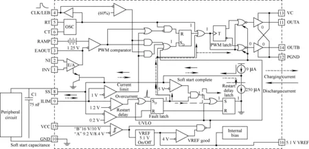
Fig.2 UC1825A single event transient effect related logic state
When the signal disturbance caused by single event propagates along path 1 (upward in Fig.2), it will be completely shut down after a period of timet1. When it propagates along path 2 (rightward in Fig.2), the process of power down/restart is completed. This period of time ist2.
In summary, if SET effect occurs in UC1825A, the typical influence process analysis on its internal logic is shown in Fig.3.
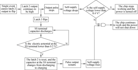
Fig.3 Typical flow chart of UC1825A single event transient effect
3 Impact of PWM single event transient effect on switching power supply of satellite payload
In order to meet the requirements of the convenience of switching on-orbit and reducing standby power consumption of backup equipment, the payload power supply basically adopts remote control commands to control the power on and off.
To achieve this function, the payload switching power supply often adopts a self-sustaining power supply mode: The core control chip PWM power supply voltage VCC is one of the output voltages of the power supply itself. The self-sustained power supply function is shown in Fig.4.
As shown in Fig.4, when the switching power supply receives a remote control command sent from the ground, the start circuit generates a 12 V voltage to supply the PWM, and the PWM generates a driving signal to make the subsequent power MOS and power transformer work. One of the windings is rectified and filtered to generate an output voltage to supply power to the subsequent electronic equipment, and the other winding is rectified and filtered through the diode D2, which replaces the start circuit to supply power to the PWM. After the command signal ends (typical time is 100 ms), the start circuit stops working to help reduce power consumption, and PWM relies on D2 to maintain normal operation.
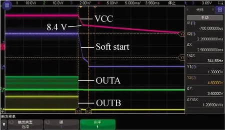
Because the PWM supply voltage VCC is one of the output voltages of the power supply, when a single event transient effect occurs, ift1 Fig.4 Schematic diagram of self-sustained switching power supply Another feature of the satellite payload power supply is that the stability of the output voltage must be ensured to avoid the transient overshoot/drop of the output voltage. Because many digital products and frequency source products have higher requirements for the stability of the power supply voltage, even a short voltage jump may cause the equipment to work abnormally. Ift2is much smaller thant1, that is, when the restart speed is faster than the power down speed obviously, the power supply will restart and resume normal operation before shutting down and the impact on the output voltage is very limited. From the previous analysis, it can be seen that ift2can be much smaller thant1, PWM will only miss very limited driving pulses, and the output voltage of the power supply will only drop slightly, which will hardly have any impact on the subsequent power-consuming equipment. By improving the PWM peripheral control circuit and reducing the discharging/charging timet2of the soft start terminal capacitor, the PWM can be restarted quickly even if it encounters a single event, and the power supply can maintain continuous operation even the output voltage is basically unchanged. The impact of single event is minimized. The method to reduce the discharging/charging timet2of the soft start terminal capacitor is to connect a resistor in series between the soft start terminal of the UC1825A and the external capacitor. The specific connection method is shown in Fig.5. The working principle of the improved circuit is: When a single event transient effect occurs in the UC1825A, the soft start terminal voltage (attention: not the voltage on the capacitor) of the chip is stepped down to 0.2 V under the discharge of the 250 μA current source, and the voltage of C27/C28 is still maintained at about 5.2 V due to the series resistance; when the soft start terminal voltage of the chip drops to 0.2 V, the reset function inside the chip is triggered, the 250 μA current source is turned off, and the 9 μA current source is used to charge the soft start terminal. At this time, also because the voltage on the capacitor has almost no change, the soft start terminal voltage will quickly (<15 μs) step back to 5.2 V. At this time,the power supply voltage of UC1825A remains above 8.4 V because of the energy storage of the capacitor at the VCC end, so that the power supply can continue to work without shutting down. Fig.5 Series resistance on soft start terminal The discharge current of soft start is typically 250 μA, if the soft start voltage drops to 0.2 V. The voltage across the capacitor remains at 5.2 V, the voltage drop across the resistor is 5 V, and the resistance value is not less than 20 kΩ. Considering that the parameters of the current source inside the chip have a certain discrete type, the resistance value can be larger. Considering that the typical value of the charging current at the soft start terminal is 9 μA during normal startup, in order not to make the voltage drop on the resistor too large during the process, the resistor value is 39 kΩ. At this time, the voltage drop of the charging current across the resistor is 0.35 V, which will not affect the soft start process of the power supply. The switching frequency of the actual test power supply is 300 kHz, and the single pulse width is 3.3 μs. When encountering a single event, no more than 5 driving pulses will be lost. The power supply voltage VCC of UC1825A is 12.3 V, the working current is 50 mA, and the power supply end filter capacitor is 10 μF. According to the calculation of formula (1), the voltage drop is 0.1 V, which has little effect. T=CV/Ι (1) Although the typical heavy ion test method can more truly reflect the actual situation of single event in space, the test preparation process is very complicated, so more and more researches tend to use pulsed laser test for evaluation and verification. Its advantage is that the laser energy and irradiation area can be accurately controlled, and the repeatability is strong[10-11]. In this study, the pulsed laser method is used for evaluation and verification, and then the heavy ion test method was used for final verification. The pulsed laser simulation test is carried out at Lanzhou Institute of Space Technology Physics. The PWM of the tested switching power supply is UC1825A, and the switching frequency is set to 300 kHz. First test the unimproved state, then after improving the PWM peripheral circuit, perform another test in the same way. During the test, pulsed laser is used to irradiate the PWM, and then monitor the drive signal output terminals of the chip: OUTA (pin 11) and OUTB (pin 14). At the same time, the soft start terminal (8 feet) and VCC power supply terminal (15 feet) are detected. The VCC supply voltage is derived from an output voltage of the power supply itself. Before the circuit improvement, as long as the laser energy reaches more than 0.3 nJ, the pulse output of the chip will be continuously missing, and the voltage of the VCC power supply terminal and soft start terminal will continue to drop. After about 800 μs, the power supply voltage VCC drops below 8.4 V, which is lower than the power supply threshold of UC1825A, and the power supply will eventually shut down completely. The typical waveform is shown in Fig.6. Fig.6 UC1825A laser pulse test waveform before improved After the circuit is improved, the pulse laser energy is gradually increased to 30 nJ, and the soft start terminal voltage drops to 0.2 V and then rebounds to 5.2 V for only 5.88 μs, which will only affect one PWM output pulse. Because the time is very short, the chip power supply voltage hardly changes. The measured waveform of the pulse laser test after the improvement is shown in Fig.7. Fig.7 UC1825A laser pulse experiment test waveform after improved The above-mentioned measured waveform fully confirms the effectiveness of this method for improving the SET effect of the power supply. Finally, in order to simulate the on-orbit working environment of the spaceborne switching power supply more realistically, the actual heavy ion test was carried out at the China Institute of Atomic Energy with the same power supply. The test results show that under the action of 5 MeV·cm2/mg, the UC1825A that does not take this measure produces continuous pulse loss, leads the product to shut down abnormally. After adopting this protection strategy, under the action of 37.2 MeV·cm2/mg, the PWM is restarted within μs level. The number of missing pulses is 1-2, which does not affect the actual work of the switching power supply product. It fully verifies the single event’s mechanism of action in PWM and the effectiveness of the protection strategy, and provides a new idea and effective method for the single event protection of this type of pulse width modulation. An important hidden danger is removed for space applications of such devices. Aiming at the switching power supply products for satellite payloads, the mechanism of the generation and propagation of single event effects in pulse width modulations are deeply analyzed, and the protection strategies and methods are proposed accordingly. The effectiveness of this strategy is shown by the pulsed laser test and the heavy ion test, which opens up new ideas for the application of such devices in special space environments.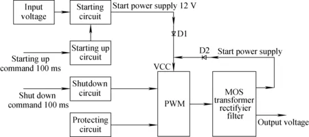
4 Single event transient effect protection strategy for space-borne switching power supply

5 Test verification

6 Conclusion
杂志排行
原子能科学技术的其它文章
- H-1NF仿星器标准磁场位形分析与高能量离子运动轨道模拟
- 铀转化生产线含氟废水处理工艺设计
- 在线进样ICP-MS用于239Pu气溶胶活度浓度连续监测技术研究
- Degradation Characteristic of Proton Irradiated 8T CMOS Image Sensor
- Comparative Experimental Study on Space Electrostatic Discharge Effect and Single Event Effect of 130 nm SOI D Flip-flop Chains
- Effects of Electron Irradiation at Different Energy and Fluences on Electrical Properties of InP HEMT Structure
