Dose Detecting of RADFETs Based on PMOS Extended to Elevated Temperature Applications
2021-12-15MAHanSUNJingHEChengfaXUNMingzhu
MA Han, SUN Jing, HE Chengfa, XUN Mingzhu
(1.Xinjiang Technical Institute of Physics and Chemistry, Chinese Academy of Sciences, Urumqi 830011, China; 2.University of Chinese Academy of Sciences, Beijing 100049, China)
Abstract: The radiation response of 100 nm- and 400 nm-RADFETs was investigated at room temperature and elevated temperatures. A total radiation dose of 80 krad(Si) was reached with two different dose rates of 3 rad(Si)/s and 0.098 rad(Si)/s. The mid-gap technique was used to separate influence of the oxide trap charge and the interface trap charge. The microscopic mechanism of radiation response at elevated temperatures was analyzed. The annealing effect of the oxide-trap charge is the main reason for the nonlinear response. The changes of the oxide-trap charge with different oxide thicknesses have great difference, while the interface-trap charge densities have little difference at elevated temperatures. The feasibility of using RADFETs at elevated temperatures was discussed, providing a reference for the application of RADFETs in elevated temperature environment.
Key words:elevated temperature condition; RADFETs; radiation response
1 Introduction
The RADFETs (radiation sensing field effect transistors) which are also called PMOS dosimeter were first proposed by Holmes-Siedle in 1974[1]. RADFETs offer many advantages over the other commonly used dosimeters for its good linearity, small volume and weight, convenient use for direct readout without delay, and low-power consumption. After years of development, RADFETs have been shown to be suitable for dose measurements in various applications such as space science, radiotherapy, nuclear industry and other conditions[2-3].
To stabilize the performance, the ambient temperature the dosimeters work at is limited. But dose measurement at high temperature conditions such as affiliated facilities in nuclear reactor and space missions is needed. The external temperature of the International Space Station can reach 120 ℃. Different solutions are used to deal with the predicament such as temperature controllers and specially designed dosimeters[4-5]. These methods cost a lot and the RADFETs can be an excellent candidate if the performance of RADFETs at elevated temperatures is fully understood.
For a calibrated RADFET, the shift of threshold voltage (ΔVth) is a function of the radiation dose received, but ΔVthis also affected by the external temperature. In order to suppress the response difference of RADFETs at different temperatures, previous researchers proposed several temperature compensation methods[6-10], including minimum temperature coefficient (MTC), differential circuit and real-time temperature feedback and other solutions. The influence of temperature onI-Vcharacteristics exists a minimum value, called MTC point, at that point the corresponding voltage can be used as a sensitive parameter to minimize the influence of temperature. However, in a large temperature range, the use of MTC is subject to many limitations, such as the change of MTC with the cumulative dose. Differential circuit is widely used as an effective temperature compensation method. Two RADFETs with the same technology are applied with different bias voltage and the difference value of ΔVthunder irradiation is taken as the sensitive parameter, thus eliminating the influence of temperature. Another way to compensate is to integrate a temperature-sensitive diode into the RADFETs to provide real-time temperature feedback, allowing for later correction of the data. However, this approach requires additional signal-processing circuits, which increase the load and instability.
The previous researches on the temperature effects of RADFETs range from -40 ℃ to 80 ℃ under irradiation[6-12]. As for higher temperatures, only the effects of post-irradiation annealing were considered. In order to develop a PMOS dosimeter suitable for elevated temperature radiation environment, the RADFETs was subjected to a comparative irradiation test under elevated temperature and room temperature conditions. The mid-gap technique was used to separate the effects of oxide-trap charge density (Not) and the interface-trap charge density (Nit)[13]. The radiation response characteristics of RADFETs under high temperature environment were studied from the microscopic mechanism. The existing problems and causes of the application of RADFETs in high temperature environment were discussed, and the basic solutions were obtained. It provides a reference and a possible method for the development and application of RADFETs at high temperature.
2 Devices under test and experimental setups
For the experiment, a set of Tyndall RADFETs with 100 nm and 400 nm gate oxide thickness was used. The chips were assembled in ceramic 14-pin DIP packages capped with kovar lids. The part consists of two identical p-channel RADFETs and two temperature sensing diodes. TheW/Lof RADFETs are 300 μm/50 μm and 868 μm/11 μm respectively. The two RADFETs have individual gate, source and drain terminals, while the bulk are connected together. Only one RADFET of each chip was tested.
All of transistors examined in this work were exposed to the total dose of 80 krad(Si) with all pins shorted during the irradiation[11-12]. To avoid the change of MTC with the cumulative dose, the gate sweep characteristics and sub-threshold sweep characteristics were tested using a KEITHLEY 4200SCS parameter analyzer after irradiation.
The experiments were performed on the cobalt-60 irradiation facility in the Xinjiang Technical Institute of Physics and Chemistry, Chinese Academy of Sciences. The panoramic cobalt-60 source and irradiation position were calibrated using a graphite cavity ionization chamber before radiation experiments. In experiment group 1, the dose rate(DR) used for different temperature conditions was 3 rad(Si)/s. Temperature chamber was used during irradiation to control the temperature of devices, and the temperature spots were 20, 80, 100, and 120 ℃. Group 2 with the DR of 0.098 rad(Si)/s and the temperatures of 20 ℃ and 100 ℃ was carried out to investigate the effects of DR at elevated temperatures. Test time was in seconds so that the NBTI effect of PMOS under test sweep voltage can be negligible.
3 Results and discussion
3.1 Threshold voltage shift and sensitivity change
The basis of RADFETs as a dosimeter is the relation between the threshold voltage shift induced by the radiation dose. The dependence of ΔVthinduced by radiation dose D can be expressed as:
ΔVth=A·Dn
(1)
whereAandnis the degree of linearity dependent on electric field, oxide thickness and absorbed radiation dose. Ideally, the dependence should be linear, which meansn=1, and in that case ‘A’ represents the sensitivitySof PMOS dosimeter:
(2)
A TID of 80 krad(Si) was reached during the irradiation stage of the experiments. The transistorVthbefore irradiation, as well as during irradiation, was determined by the transfer characteristics. The ΔVthwith cumulative dose at different temperatures of 400 nm-RADFETs is shown in Fig.1a. The slope at each point was calculated to obtain the sensitivity. The relationship between the sensitivity and the cumulative dose is shown in Fig.1b. It can be seen that for 400 nm-RADFETs,the sensitivity is much high at low total dose under high temperature environment, up to 0.35 mV/rad(Si), and the difference between the sensitivity under room temperature condition is up to 0.1 mV/rad(Si). With the increase of total dose, the sensitivity of the device decreases continuously. The sensitivity at elevated temperature decreases more obviously with the cumulative dose, for the sensitivity at high temperature is lower than that at room temperature when the total dose is higher than 30 krad(Si).
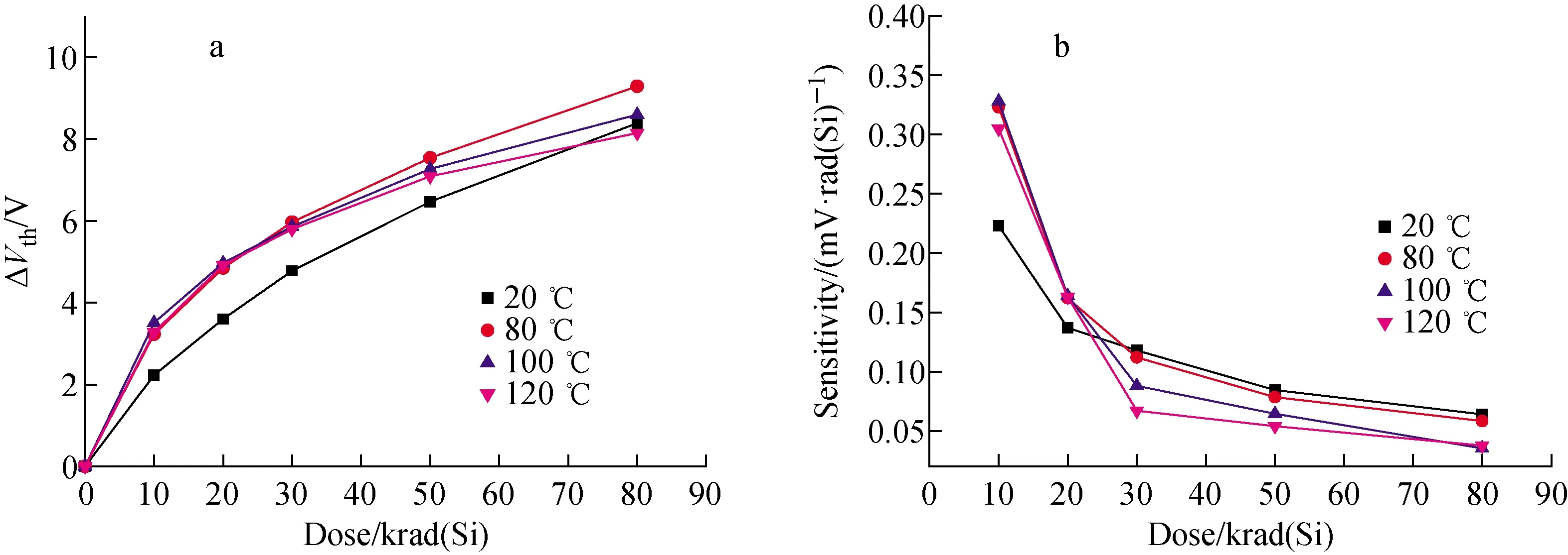
Fig.1 Characteristic change of 400 nm-RADFETs at different temperatures
The ΔVthand sensitivity change with cumulative dose of 100 nm-RADFETs are shown in Fig.2a and Fig.2b, respectively.
For 100 nm-RADFETs, due to the thin gate oxide thickness, the total energy deposited by gamma rays in the oxide layer is reduced, and the total number of electron hole pairs generated is reduced. Therefore, a larger measurement range can be achieved, but the sensitivity of response is also reduced. In the low total dose range, the sensitivity is only 0.02-0.035 mV/rad(Si), which is about 1/10 of the 400 nm-RADFETs. In the measurement range, the sensitivity of 100 nm-RADFETs decreases less, that means, the linearity of 100 nm-RADFETs is better. At high temperatures, the 100 nm-RADFETs has improved sensitivity while achieving better linearity.

Fig.2 Characteristic change of 100 nm-RADFETs at different temperatures
3.2 Effects of oxide-trap charge and interface-trap charge
The threshold voltage drift of MOS device caused by irradiation is mainly caused by trap charge buildup and annealing in gate oxide layer[14-18]. In order to explain the difference of sensitivity change, the mid-gap technique was used to separate the ΔVthcaused by oxide-trap charge and interface-trap charge[13]. Equations (3)-(5) are used to calculate the changes ofNotandNit:
ΔVth=ΔVit+ΔVot
(3)
(4)
(5)
The ΔNotand ΔNitof 400 nm-RADFETs with the cumulative dose at different temperatures are shown in Fig.3a and Fig.3b respectively. It can be seen that the annealing of the oxide traps charge is obvious, and high temperatures intensify the annealing effect. The change of the interface-trap charge can maintain a good linearity, and it has certain annealing at high temperature and high dose, for it reaches a maximum between 80 ℃ and 120 ℃.
Numbers of theories and models have been reported for the discussion of traps charge buildup and annealing[14-15]. TheE′ center model and the dipole hypothesis were effective in explanation of hole traps activities in oxide, the energetic particles passing through the oxide layer generate electron-hole pairs.
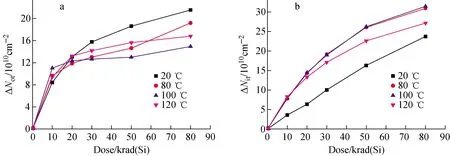
Fig.3 Characteristic change of 400 nm-RADFETs at different temperatures
Within the time of picoseconds after electron-hole pairs are created, most of the electrons will rapidly drift toward the gate. And holes will drift toward the SiO2/Si interface slowly. As the holes approach the interface, some fraction of holes will be trapped, forming a positive oxide-trap charge for the existent of large amounts of vacancies. Generally, trapped holes annealing can proceed by either of two processes, tunneling or thermal excitation. Tunneling is the dominant mechanism at room temperature, while the thermal excitation will eventually dominate at elevated temperature, so that the annealing of oxide trap charge at elevated temperature will be intensified.
The interface-trap charge buildup is mainly explained by hydrogen transport model[16-18]. In the process of irradiation, some protons will be released by the gate oxide, and the protons will be transported to the SiO2/Si interface through the jump between the potential wells. The high temperature will accelerate this transport process. After reaching the interface, protons will move laterally along the interface due to the potential barrier of SiO2/Si interface and may be captured to form the interface trap charge. AsNitincreases, protons may form Si—H bonds with Si suspension bonds and eliminate an interface-trap charge, until the interface-trap charge generated and eliminated to form an equilibrium state. The study results of Rashkee et al. show that the dependence of the interface states to establish equilibrium state and temperature during the irradiation process will reach a maximum between 80 ℃ and 150 ℃[17]. For 100 nm- and 400 nm-RADFETs, the maximum value is between 80 ℃ and 120 ℃, because theNitincrement at 120 ℃ has shown a downward trend at high doses.
The ΔNotand ΔNitof 100 nm-RADFETs with cumulative dose at different temperatures are shown in Fig.4a and Fig.4b. It can be seen that as the thickness of gate oxide becomes thinner, both the oxide-trap charge and the interface-trap charge at room temperature become much smaller for the decrease of total deposition energy. At high temperatures, ΔNotis about 1/3 of that of 400 nm-RADFETs, but the difference between the interface-trap charge density is not so great, and the difference of ΔNitbetween 100 nm-RADFETs and 400 nm-RADFETs at the total dose of 80 krad(Si) at 100 ℃ and 120 ℃ is less than 5%. This result can be interpreted by that the proton transport distance to the interface becomes shorter, which makes the interface states increase faster, thus compensating for the decrease in proton release caused by the decrease in total deposited energy. And it should be noted that the difference in the distribution of the internal electric field when the gate oxide thickness becomes thinner leads to the difference in the recombination rate of the generated electron-hole pairs. Johnston et al. studied the dependence between the charge yield and the electric field at different temperatures based on the Onsager model[19]. This is also the reason for increased sensitivity at high temperatures. The trap charge produced in the thin oxide layer modulates the internal electric field more obviously.
3.3 Effects of dose rate
An experiment group with low dose rate (LDR) of 0.098 rad(Si)/s at 20 ℃ and 100 ℃ was used as a comparation to the high dose rate (HDR) of 3 rad(Si)/s, and the ΔVthresults were shown in Fig.5.
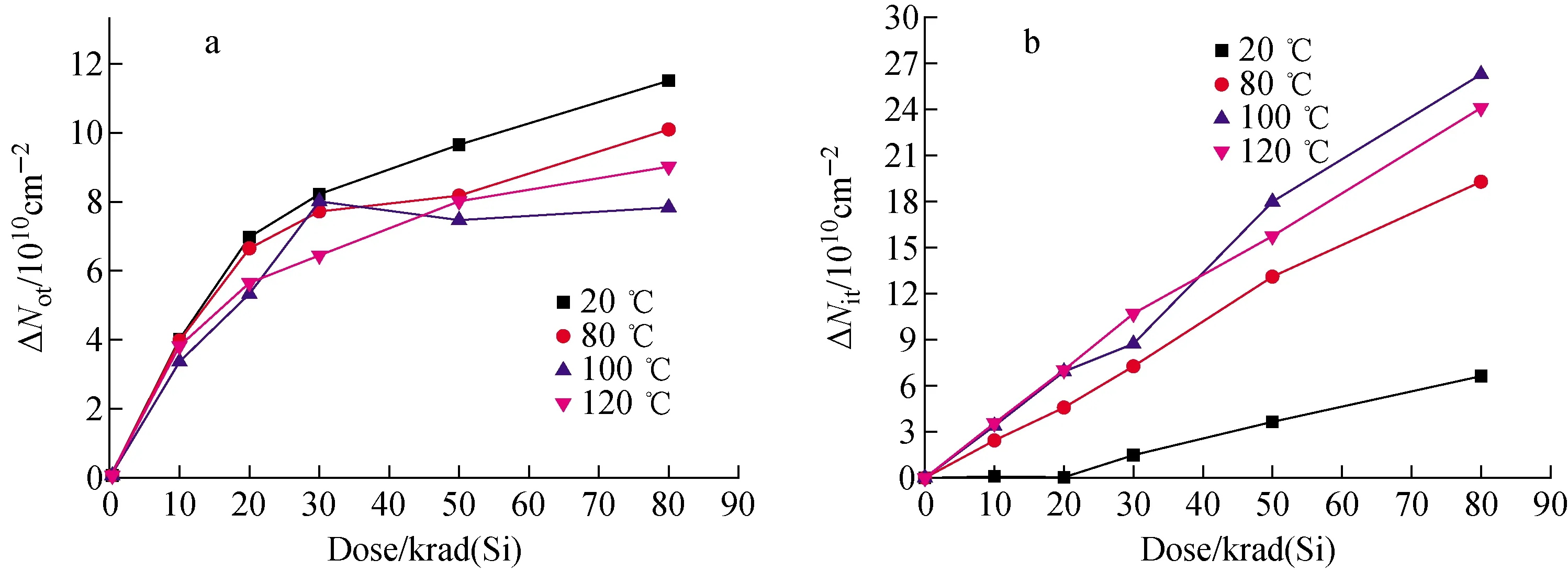
Fig.4 Characteristic change of 100 nm-RADFETs at different temperatures
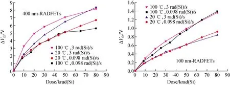
Fig.5 ΔVth with different DR
It can be seen from Fig.6 that the ΔVthof 400 nm-RADFETs at LDR was lower than HDR, and the difference between 20 ℃ and 100 ℃ at LDR was quite small up to 50 krad(Si). For 100 nm-RADFETs, the ΔVthat LDR was close to HDR, and the effect of temperature was the same. For the LDR condition, a longer irradiation time could make a greater annealing of oxide-traps charge and the greater buildup of interface-traps charge for both 100 nm- and 400 nm-RADFETs. The ΔNotand ΔNitby MGT at different DR of 400 nm- and 100 nm-RADFETs were displayed in Fig.6 and Fig.7, respectively.
An exception was found that for 400 nm-RADFETs at 100 ℃, the interface-traps charge buildup of LDR was smaller than HDR. This is because proton loss processes limit the increased buildup at elevated temperatures[18]. Irradiation with LDR at elevated temperatures reached a high concentration of molecular hydrogen at lower cumulative dose, which passivated the interface-traps. For 100 nm-RADFETs, the low concentration of hydrogen in thinner oxide and fewer radiation-induced hole activities make them show very little enhanced passivation at elevated temperatures.
The experimental data and microcosmic mechanism indicated that RADFETs are suitable for using as a dosimetric sensor to the applications at elevated temperature. The dose response of RADEFTs at elevated temperatures still keeps a good mathematic relation with cumulative dose. In the LDR environment such as space, 400 nm-RADFETs show higher radiation sensitivities and independence on temperature when doses were below 50 krad(Si). For an environment where the dose rate changes, 100 nm-RADFETs can be quite suitable because of its stability to dose rate and a better linearity at different temperatures and DR which make them more convenient using calibration data. A calibration of certain temperature range and the real-time temperature feedback by temperature-sensitive diode are needed for RADFETs using in actual elevated temperature environments. A combination of RADFETs with different gate oxide thicknesses can achieve more accurate measurement.
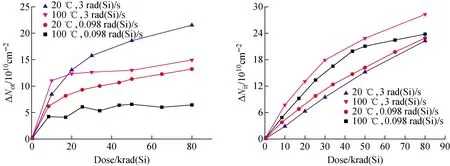
Fig.6 Characteristic change of 400 nm-RADFETs at different DR
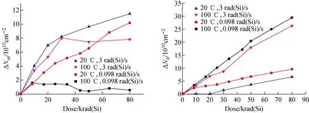
Fig.7 Characteristic change of 100 nm-RADFETs at different DR
4 Conclusion
A wider temperature range that 100 nm- and 400 nm-RADFETs could be applicative was investigated. A total radiation dose of 80 krad(Si) was reached with two different dose rates of 3 rad(Si)/s and 0.098 rad(Si)/s. Three main results were obtained. Firstly, 100 nm-RADFETs perform more stably and linearly at different temperatures and dose rates, while 400 nm-RADFETs show higher sensitivity and independence on temperature below 50 krad(Si) at LDR. Secondly, the sensitivity decreased with the dose accumulation, and that is worse in elevated temperature and thicker oxide. Thirdly, the annealing effect of oxide-trap charge is the major cause of nonlinear response, while the ΔNitcan keep good linearity. At elevated temperature, the difference of ΔNitbetween 100 nm- and 400 nm-RADFETs is small, the built-in electric field distribution and the kinetics of proton activities could be the influencing factors. It can be concluded that in the mentioned temperature range, the adequate response of RADFETs ensure an effective use of them in dosimetry.
杂志排行
原子能科学技术的其它文章
- H-1NF仿星器标准磁场位形分析与高能量离子运动轨道模拟
- 铀转化生产线含氟废水处理工艺设计
- 在线进样ICP-MS用于239Pu气溶胶活度浓度连续监测技术研究
- Degradation Characteristic of Proton Irradiated 8T CMOS Image Sensor
- Comparative Experimental Study on Space Electrostatic Discharge Effect and Single Event Effect of 130 nm SOI D Flip-flop Chains
- Effects of Electron Irradiation at Different Energy and Fluences on Electrical Properties of InP HEMT Structure
