Influence of Ti3C2Tx (MXene) on the generation of dielectric barrier discharge in air
2021-11-30WeishengCUI崔伟胜QiaoluLIN林俏露HongboLI李宏博ShuaiZHAO赵帅YungeZHANG张赟阁YifanHUANG黄逸凡ShutingFAN范姝婷YilingSUN孙一翎ZhengfangQIAN钱正芳andRenhengWANG王任衡
Weisheng CUI (崔伟胜), Qiaolu LIN (林俏露), Hongbo LI (李宏博),Shuai ZHAO (赵帅), Yunge ZHANG (张赟阁), Yifan HUANG (黄逸凡),Shuting FAN(范姝婷),Yiling SUN(孙一翎),Zhengfang QIAN(钱正芳) and Renheng WANG (王任衡)
1 Key Laboratory of Optoelectronic Devices and Systems of Ministry of Education and Guangdong Province, College of Physics and Optoelectronic Engineering, Shenzhen University, Shenzhen 518060,People’s Republic of China
2 Aerospace Information Research Institute, Chinese Academy of Sciences, Beijing 100094, People’s Republic of China
3 Shenzhen Institutes of Advanced Technology,Chinese Academy of Sciences,Shenzhen 518055,People’s Republic of China
Abstract The formation of homogeneous dielectric barrier discharge (DBD) in air is a key scientific problem and core technical problem to be solved for the application of plasmas.Here,we report the effect of two-dimensional (2D) nanomaterial Ti3C2Tx (Tx = –F, –O and/or –OH) on regulating the electrical discharge characteristics.The field emission and weak bound state property of Ti3C2Tx can effectively increase the seed electrons and contribute to the generation of atmospheric pressure homogeneous air DBD.The electron avalanche development for the uneven electrode structure is calculated, and the discharge mode transition is modeled.The comparative analyses of discharge phenomena validate the regulation of Ti3C2Tx on the discharge characteristics of DBD.The light emission capture and the voltage and current waveforms verify that the transition of Townsend discharge to streamer discharge is effectively inhibited.The optical emission spectra are used to characterize the plasma and confirm that it is in a non-equilibrium state and the gas temperature is at room temperature.This is the first exploration of Ti3C2Tx on the regulation of electrical discharge characteristics as far as we know.This work proves the feasibility of Ti3C2Tx as a source of seed electrons to form homogeneous DBD, establishing a preliminary foundation for promoting the application of atmospheric pressure non-equilibrium plasma.
Keywords: atmospheric pressure air plasma, Townsend discharge, seed electron, Ti3C2Tx
1.Introduction
Non-equilibrium plasma normally has a low temperature and can generate a large number of high-energy active particles and ultraviolet radiation,which are vital for the application in material surface modification [1–3], synthesis of nanomaterials [4, 5], and biomedical sterilization [6–8], etc.Dielectric barrier discharge (DBD) is an essential approach for the industrial application of non-equilibrium plasma with its properties of simplicity, reliability, and scalability.To improve the discharge uniformity, the DBDs are mostly operated at low pressure and/or depend on noble gas circumstances [9, 10], which brings some limitations such as materials being subject to vacuum processing and the high economic costs.The DBD obtained in air at atmospheric pressure usually exhibits streamer discharge mode,which will reduce the treatment effect in the material modification and even cause damage to the materials being processed[11,12].
It has been known that the discharge characteristics of DBD at atmospheric pressure mostly depend on the development condition of electron avalanche, which is determined both by the time scales and spatial scales of the development.By utilizing nanosecond voltage pulse,the electron avalanche development and its following process can be inhibited, and the diffuse discharge showing better uniformity is achieved[13–15].However, the nanosecond pulsed power supply developed in recent years is costly and limited in power.Besides, its discharge characteristics are susceptible to specific discharge electrode structures because the nanosecond voltage rise time is sensible to the specific capacitive load,which may cause inconformity and are not beneficial for high power industrial application.The power supply with a low frequency (for example, less than 50 kHz) is the possible choice for the large-scale application of atmospheric pressure air DBD.Whereas the voltage pulse of the low-frequency power supply cannot restrict the overdevelopment of the electron avalanches on the time scale, the discharge easily transited to streamer discharge.The mean free path of electron colliding with gas molecules in the air is only 68 nm[16].The atmospheric pressure homogeneous air discharge with a low-frequency power supply is severely limited by gap size and concluded to be found in gaps of less than 5 mm[17–20].
The seed electrons have been proved to have a significant impact on the formation of homogeneous DBD at atmospheric pressure [10, 15, 21–23].The design of inhomogeneous electric field distribution can produce local additional seed electrons and is beneficial for the uniformity of DBD[24–27].By constructing a unique curved-plate electrode,we managed to produce a relatively homogeneous atmospheric pressure DBD in previous research [28].In addition, the‘shallow traps’ [29] on some dielectrics can also supply seed electrons and improve the discharge homogeneity of DBD.Luo et al [30] used unique alumina ceramics plates as dielectric barriers and achieved a homogeneous Townsend discharge in air at atmospheric pressure condition.However,the discharge was so weak that hardly visible for naked eyes[31] and cannot withstand a reliable industrial application.Finding other way of supplying a high density of seed electrons is the key to forming a practically applicable homogeneous discharge under atmospheric pressure air condition.
Two-dimensional (2D) nanomaterials have distinct characteristics of ultra-high specific surface area, surface and boundary effect, and quantum size effect compared with the traditional bulk materials [32, 33].The new family of 2D nanomaterial Ti3C2(MXene) discovered in 2011 has highly adjustable chemical and structural forms because of its elemental compositions and surface terminations [34–36].Pristine Ti3C2exhibits particular electrical conductivity due to its special combination of metallic and covalent bonds [37].However, the absorption of different terminals changes the density of states (DOS) and therefore endows the Ti3C2Tx(Tx= –F, –O and/or –OH) with different mechanical, thermal, electromagnetic, and optical properties.
It has been reported that the Ti3C2Tx(MXene) based material is capable of high field electron emission property[38, 39].However, the impact of Ti3C2Txon regulating the electrical discharge has never been reported.Here, we investigate the influence of 2D nanomaterial Ti3C2Txon the atmospheric pressure air DBD.Based on theoretical calculation and experimental verification, it is inferred that the electron field emission properties and the particular weak bound states of Ti3C2Txcan regulate the electrical characteristics of the DBD.The combined effect of inhomogeneous electric field distribution and Ti3C2Txcan eventually achieve a homogeneous air Townsend discharge.
2.Experimental setup
The Ti3C2Txused in this study was fabricated by etching Ti3AlC2in HF solution.The chemical reagents were used without further treatment after the purchase and they are all in analytical grade.The Ti3AlC2powder (400 mesh) was purchased from Suzhou Beike 2D materials Co., Ltd, China.The HF solution was purchased from Shanghai Aladdin Bio-Chem Technology Co., Ltd, China.The main fabrication procedures are as follows: 2 g of Ti3AlC2powder was placed in 20 ml of 40 wt%HF solution and stirred for 12 h at 25°C.The obtained solution was centrifuged, and the sediment was selected and washed several times with deionized water to remove the remaining acid(until the solution pH reaches 6).The sediment was sonicated to obtain the exfoliated Ti3C2Tx, and then the Ti3C2Txfilm was obtained by vacuum filtration and dried in a 70°C vacuum drying oven.The flow chart is shown in figure 1.

Figure 1.Flow chart for the fabrication of Ti3C2Tx.
An uneven electrode structure with a maximum gap of 3 mm was designed, as shown in figure 2.The electrode structure consists of two identical Polytetrafluoroethylene(PTFE) plates (20 mm × 30 mm × 2.5 mm), which were vertically placed together.An arc-shaped groove was carved on each of the contact surfaces,forming an uneven discharge gap.The length and the width of the gap were 12 mm and 20 mm, respectively.The maximum size of the gap was 3 mm.The Ti3C2Txfilm(with a width of 6 mm and thickness of less than 0.2 mm) was fixed on one side of the groove.Both the high-voltage electrode and the ground electrode are made of copper sheets (6 mm × 30 mm × 0.02 mm), and were fixed in the center of the dielectrics’ outer surface.The CTP-2000K was adopted as the power supply, which has a sinusoidal high voltage output with a frequency of 6 kHz and a maximum output voltage of 30 kV.The applied voltage was measured by a capacitive voltage divider and the total discharge current flowing through the electrodes was obtained by a resistor with 50 Ω,which were presented by an oscilloscope(TBS 1102B).The discharge experiments were performed in ordinary air circumstance,and the environmental temperature,air humidity, and gas pressure are 25 °C, 80%, and 1.01 × 10⁵Pa, respectively.

Figure 2.Schematic diagram of (a) the experimental arrangement and (b) the electrode structure.(c) The picture of the T3C2Tx film.
3.The electronic characteristics of Ti3C2Tx
The Ti3C2has been reported to have a low work function value of 4.6 eV and 3.7 eV by Alshareef et al [40] and Carlo et al [41], respectively.The field emission occurs at an electron current density of 0.02 mA cm−2with an electric field of 5 × 10⁴V cm−1reported by Yan et al[39].The turnon electric field resulting in a current density of 0.1 mA cm−2of planar Ti3C2emitter is 7.6 × 10⁴V cm−1during the increase of voltage,and the standing Ti3C2emitter exhibits an electron current density of 59 mA cm−2with the applied electric field of 7.5 × 10⁴V cm−1[39].Liang et al [38] further discovered that the Ti3C2Txcan also have a current density of 0.05 mA cm−2with a turn-on field of 10.3 × 10⁴V cm−1.After removing –F terminals by plasma treatment, the maximum current density increases to 1.22 mA cm−2, and the turn-on field reduces to 8.5 × 10⁴V cm−1, which is close to that of pristine Ti3C2.The field emission mechanism can directly provide a large number of free electrons, which is vital for improving the characteristics of the electrical discharge.
Apart from the terminals, the Ti vacancies will also be formed on the surface of Ti3C2Txduring the fabrication process[42,43].The terminals and Ti vacancies can tune the electronic properties of Ti3C2and, therefore, may exert an impact on the surface electrons.The density functional theory(DFT) calculation was carried out to obtain its extra-nuclear electron distribution.In the calculation, 2 × 2 × 2 supercell with 16.6% surface Ti vacancy or terminals was used as original geometric model.The cut off energy was set in 500 eV, and the Monkhorst-Pack scheme k points were 5 × 5 × 1.The fabricated Ti3C2Txwas also characterized by x-ray photoelectron spectroscopy (XPS).The XPS spectra and the DOS of Ti3C2Txare shown in figure 3.
As shown in figure 3(a), the F 1s, O 1s, Ti 2p, and C 1s peaks are observed from the large energy range spectra of Ti3C2Tx.The F 1s near 686 eV and O 1s near 530 eV indicate the existence of–F,–O and–OH terminals,respectively.The presence of Ti–C bond and two Ti–O bonds(corresponding to OH-TiC and O-TiC, respectively) is also evident near the binding energy of 464 eV, 459 eV and 455 eV, respectively[44].According to the calculation of DFT, it has been found that the DOS of bare Ti3C2passes through the Fermi surface,indicating the metal-like conductivity.However, it changes significantly with Ti vacancy and the terminals on the surface of Ti3C2Tx.As shown in figure 3(b), when Ti vacancy exists on the Ti3C2surface, a defect state peak is introduced at−0.3 eV below the Fermi level, which is mostly aroused by the p orbital electrons for C.The defect state peak also appeared at about −1 eV below the Fermi level when Ti3C2are terminated with–F,–O or–OH,and these defect states are contributed mostly by d orbital electrons,which come from Ti or the hybrid interaction of Ti and terminals.These local defect states are donor-type defects and would form a weak bound effect on the electrons.The weak bound states were supposed to supply additional electrons for the discharge,similar to the mechanism of shallow traps [45].In addition,the 2D nanomaterials have a far greater specific surface area compared with the traditional dielectric barriers, which will enhance the supplement of seed electrons compared with the bulk dielectrics.

Figure 3.(a) The XPS spectra of fabricated Ti3C2Tx sample and (b) the DOS of Ti3C2Tx with vacancy and terminals of –F, –O, and –OH.
4.Results and discussions
4.1.Theoretical analysis and modeling
The electric field distribution in the uneven electrode differs from that in the plate electrode due to the inhomogeneous electrode structure.To characterize the electric field distribution of the uneven electrode, the ANSYS Maxwell software was used to conduct the electric field simulation with a voltage of 11 kV.The Ti3C2Txexhibited semiconductor characteristics with the tuning of the surface terminals[46, 47]; therefore, a typical silicon film was used instead in this simulation.
It can be seen from figure 4 that the electric field strength exhibited inhomogeneous distribution characteristics.The maximum of the electric field strength appeared in the narrow gaps (4.4 × 10⁴V cm−1), and it declined with the increase of the gap size.By comparison, the electrode with Ti3C2Txfilm exhibited increased electric field strength up to 6.8 ×10⁴V cm−1.It should be noted that the usually sub-micro size Ti3C2Txflake was not constructed in the simulation due to the parameter restriction caused by centimeter electrode size.The electric field on the Ti3C2Txflake edge will be significantly enhanced due to the submicron structure according to the Fowler–Nordheim theory[48,49].The value of enhancement factor β is estimated to be more than 1000 by the research of Liang et al[38].Therefore,it is possible for the Ti3C2Txflake to reach the field emission turn-on field with the applied voltage of kilovolts.
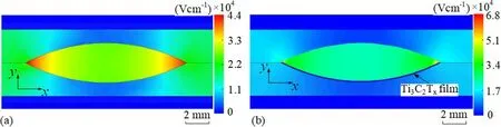
Figure 4.The electric field strength distribution of the uneven electrode (a) without and (b) with the Ti3C2Tx film.The Ti3C2Tx was represented by silicon due to its semiconductor property.Besides,the sub-micro size of Ti3C2Tx flake was not constructed in the simulation due to the software parameter restriction caused by centimeter electrode size.
The electron avalanches development of the uneven electrode with and without the Ti3C2Txfilm were analyzed.The Y-axis’s positive direction was set as the development direction, and multiple paths were arranged along the X-axis to explore the development of electron avalanches in different positions.The viable seed electrons of the uneven electrode without the Ti3C2Txwere assumed to be 0.01 of the surface electron density considering the incomplete release of trapped electrons.The field emission charges (0.37 pC mm−2) within a period of electron avalanches development (about 30 ns)were obtained as seed electrons based on the field emission current density of 1.22 mA cm−2of Ti3C2Txfilm.According to the modeling method reported in previous research [28],the electron avalanche development and the discharge mode transition pattern of the uneven electrode with the preset seed electrons can be estimated by the iterative computations with MATLAB.
During the development,if the electron avalanche arrives at the upper surface without reaching the Meek criterion, it will stay Townsend discharge mode.In contrast, if the electron avalanche reaches the Meek criterion before it arrives at the upper surface, it will transit to a streamer.The electric field distribution of the gap caused by produced space charges after the electron avalanche development is depicted in figure 5.
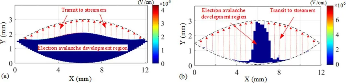
Figure 5.The space charge electric field distribution of the uneven electrode (a) without and (b) with the Ti3C2Tx film caused by produced space charges after the electron avalanches development under the voltage of 11 kV.The black dash line denotes the outline of the gap.The path interval was set at 0.2 mm to ensure the independent development of electron avalanches according to [20].The red dotted arrows indicate that the electron avalanches have transited to streamers.
It can be seen in figure 5 that the electron avalanches in different positions of the gap without Ti3C2Txfilm exhibited less differences.The electron avalanches in narrow gaps transit to streamers at a shorter distance as the electric field strength is higher.The ones in central regions of the gap transit to streamers at a longer distance with a lower electric field.However, the electron avalanche transition of the gap with the Ti3C2Txfilm exhibits an entirely different pattern.The electron avalanches in the narrow gaps transit to a streamer due to a higher electric field strength and the more seed electrons from field emission.While parts of the electron avalanches in the central region stay Townsend discharge mode.
The variation tendency of the electron avalanche transition distribution in the gap with different applied voltages was further investigated, as shown in figure 6.
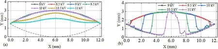
Figure 6.The distribution of electron avalanche transition for the uneven electrode(a)without and(b)with the Ti3C2Tx film under different voltages.The black dash line denotes the outline of the gap.The transition points of electron avalanche with the same voltage were connected to illustrate the variation tendency and differ from each other.
It can be seen from figure 6 that the theoretical analysis predicted different discharge transition characteristics for the gap with and without the Ti3C2Txfilm.The transition of electron avalanches appeared first at about 10 kV and covered most of the central regions simultaneously with a higher voltage, which may lead to the occurrence of streamer discharge.By comparison,the electron avalanche transition with Ti3C2Txfilm first appeared in the narrow gaps and expanded gradually to the central region as the voltage increases.The existence of Ti3C2Txfilm can regulate the discharge mode transition and restrain the abrupt occurrence of large area discharge mode transition.
Actually, the electric field strength in the narrow gaps is higher than that in the central region, which would lead to enhanced field emission of Ti3C2Tx.Therefore,the regulation effect on the discharge mode transition should be more pronounced.Furthermore,the weak bound states of Ti3C2Txfilm and the diffusion of electrons in the narrow gaps can effectively increase the seed electrons density in the central region.The increased seed electrons density is crucial for the formation of homogeneous Townsend discharge at high gas pressure [12].
4.2.Discharge phenomena
The experiments were carried out to verify the influence of Ti3C2Txon the discharge,as shown in figure 7.The discharge phenomena of the gap and the light emission analyses with short exposure were depicted and analyzed.It can be seen from figures 7(a)–(c) that the uneven electrode exhibited the characteristics of streamer discharge.The visible discharge first appeared near the narrow gaps when the voltage was above 10 kV, and then expanded to the central region as the voltage increases.Finally,the whole gap except the narrowest positions showed distinct streamer discharge with higher applied voltage, which is consistent with the forecast of the theoretical analysis.The light emission images and the data analysis with the exposure time of 2000 μs,1000 μs,and 500 μs (minimum of three cycles) detail the specific discharge filaments in the gap.It is confirmed that the uneven electrode exhibited streamer discharge characteristics.
By comparison, the uneven electrode with Ti3C2Txfilm revealed quite different discharge characteristics,as shown in figures 7(d)–(f).The visible discharge first happened in the narrowest gap at about 10 kV and grew gradually to the central region as the voltage increases.The discharge in central region exhibited diffuse and mild characteristics,which is different from the bright filaments presented in figure 7(a).Ultimately,most of the whole gap presented a soft and homogeneous discharge.There are no visible discharge filaments except for the narrowest gaps.The light emission images with short exposure were found to be very weak and presented no filaments.Only the upper periphery of the gap revealed a weak luminous layer.The data analysis of light emission images did not present any evidence of the discharge filaments’existence in the gap space.It is inferred that the soft and homogeneous discharge phenomena are accumulated by the weak Townsend discharge in each discharge cycle,and no streamer discharges were produced with the Ti3C2Txfilm.
In addition, it should be pointed that the theoretical modeling in the gap was not completely corresponding with the discharge phenomena, as it was simplified and did not consider the mutual interaction of electron avalanches.The effects of additional seed electrons supplied by the weak bound states and the narrow gaps were hard to be taken into account in the calculation quantitatively.Furthermore, the merging of electron avalanches before it transits to streamers may also affect the formation of streamers[12].However,the theoretical analysis reflected the change patterns of discharge mode and proved that the Ti3C2Txcould alter the transition of electron avalanche effectively.The comprehensive effect of inhomogeneous electric field distribution and the Ti3C2Txfilm achieved an enhanced homogeneous Townsend discharge in air at atmospheric pressure.
4.3.Electrical characteristics
The voltage and current waveforms corresponding to the discharge phenomena were recorded and analyzed, as illustrated in figure 8.It can be seen from figure 8 that the current waveform had some‘spikes’with a duration of 1–2 μs when the gap is without Ti3C2Txfilm,which indicates the formation of discharge filaments.However, when Ti3C2Txfilm was set on the dielectrics, the number of spikes in the current waveform was mostly eliminated.It indicates that the electron avalanche transition in most of the gap is inhibited effectively,and most of the gap remains in Townsend discharge mode.According to the discharge phenomena and the characteristics of current waveform, the improvement of Ti3C2Txon the discharge uniformity is confirmed.The increase of seed electrons is assumed to be responsible for the enhancement of the uniformity of the DBD.
4.4.Optical emission spectra
The optical emission spectra (OES) of the generated plasma were characterized by a spectrometer (Princeton Instruments SP2500).The resolution of the spectra is 0.02 nm (grating:1200 g mm−1;slit width:20 μm).As shown in figure 9(a),the emission spectra with a wavelength of 300–480 nm were recorded,and the excited OH,N2,andwere depicted.The excited N2,and reactive OH are produced by the collision of high-energy electrons with nitrogen molecules and water molecules in the environments[15].The gas temperature can be estimated by the rotational temperature of plasma [50],which was procured by fitting the simulated spectra of the second positive bands of N2(C3Πu→ B3Πg, Δυ = -2)with the experimental spectra through the Specair software[51–53], as shown in figure 9(b).
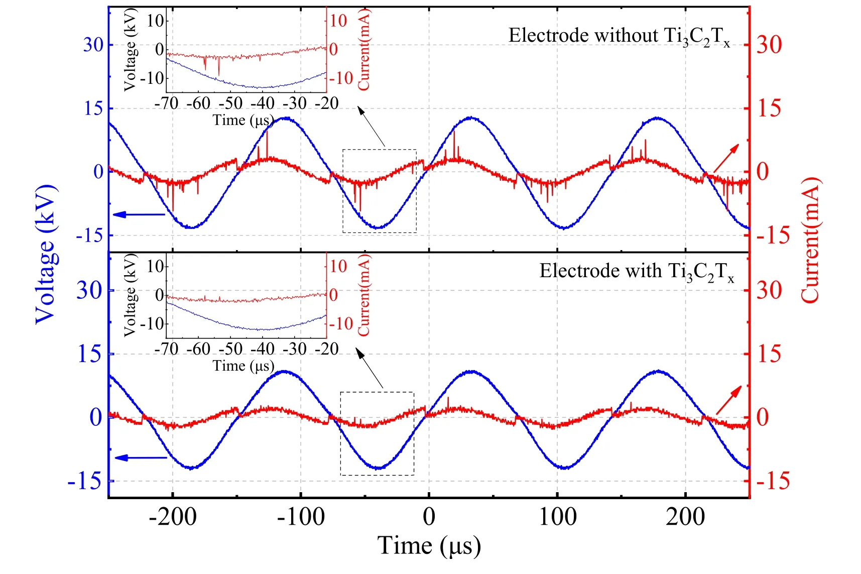
Figure 8.The discharge waveforms of the electrode with full discharges.
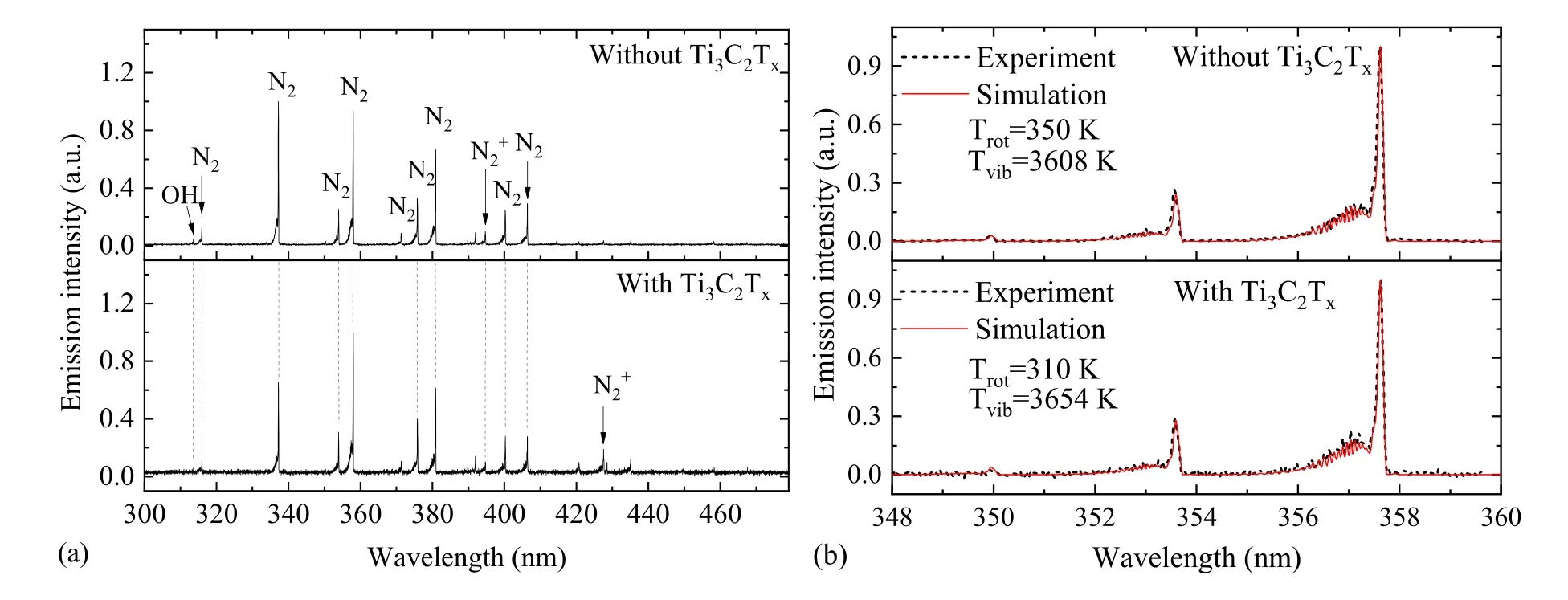
Figure 9.(a) OES of the discharge under atmospheric pressure air condition and (b) the rotational and vibrational temperature procured by fitting the simulated spectra of the N2 ( C 3 Π u → B3 Π g , Δυ = -2)with the experimental spectra.
As one can see from figure 9(b)that the obtained plasma is under non-equilibrium conditions with much higher vibration temperature compared with rotational temperature.The Trottemperature of electrode structure with Ti3C2Txfilm is about 310 K, which is lower than the temperature when Ti3C2Txfilm was not set by more than 40 K.The decrease of gas temperature proved that the fierce discharge filaments were inhibited and the role of Ti3C2Txin improving the uniformity of the discharge was further confirmed.In addition, the structure properties of Ti3C2Txflakes will not be affected by the room temperature[37,54,55],which ensured the validity of the effectiveness of continuity.The discharge characteristics of fabricated Ti3C2Txlayer were tested to be effective for weeks when stored in dry circumstance.The lower gas temperature of electrode structure with Ti3C2Txfilm also contributes its industrial application such as biomedical sterilization and surface treatments.
5.Conclusions
In summary, the impact of 2D nanomaterial Ti3C2Txon the generation of atmospheric DBD was analyzed.We found that the weak bound states formed on the Ti3C2Txsurface and the field emission property can contribute to the formation of atmospheric pressure homogeneous air DBD.The discharge experiment verified the validity of the preceding theoretical analysis.The spectra data reveal that the plasma temperature is at room temperature, which is conducive to its industrial application.This is a particular mechanism by which Ti3C2Txaffects the electrical discharge.This study can provide introductory insights of Ti3C2Txin the field of electrical discharge, and serves as a significant foundation to further realize the atmospheric pressure homogeneous air plasmas.
Acknowledgments
We would like to thank the support of the Science and Technology Innovation Commission of Shenzhen (Nos.JCYJ20180507181858539 and JCYJ20190808173815205),Guangdong Basic and Applied Basic Research Foundation(No.2019A1515012111),Shenzhen Science and Technology Program (No.KQTD20180412181422399), the National Key R&D Program of China (No.2019YFB2204500),and National Natural Science Foundation of China (No.51804199).
ORCID iDs
杂志排行

Plasma Science and Technology的其它文章
- Spatial and temporal evolution of electromagnetic pulses generated at Shenguang-II series laser facilities
- Numerical study on the loss of fast ions produced by minority ion cyclotron resonance heating in EAST
- Machine learning of turbulent transport in fusion plasmas with neural network
- Observation of coherent mode induced by a molybdenum dust on EAST
- Investigation of stimulated Raman scattering in longitudinal magnetized plasma by theory and kinetic simulation
- The influence of magnetic field on the beam quality of relativistic electron beam long-range propagation in near-Earth environment