Buck converter stability techniques for secondary filters and adaptive voltage positioning
2021-10-21YaoSuyiJiangJianguo
Yao Suyi Jiang Jianguo
(School of Electronic Information and Electrical Engineering, Shanghai Jiaotong University, Shanghai 200240, China)
Abstract:To reduce output voltage noise and improve dynamic response performance, this study designed a buck converter on the basis of secondary filters and adaptive voltage positioning (AVP). A hybrid control method was proposed for the compensation of the secondary filter. The introduction of a high-frequency feedback path, in addition to the traditional feedback path, effectively improved the influence of the secondary filter on the loop stability and direct current regulation performance. A small-signal model of the buck converter based on the proposed control method was derived, and the stability and selection of control parameters were analyzed. AVP is realized using an easy-to-implement and low-cost control method that was proposed to improve dynamic response performance by changing the low-frequency gain of the control loop and load regulation of the output voltage. The experimental results of the buck converter showed that the proposed method effectively reduced the output voltage noise by 50% and improved the dynamic response capability to meet the target requirements of mainstream electronic systems.
Key words:buck converter; secondary filter; adaptive voltage positioning (AVP); output voltage noise; small-signal model
With the gradual popularization of 5G and the growing demand for autonomous driving systems, buck converters with high power density and low noise have been widely used. At present, the radar systems in 5G communication systems and autonomous driving systems not only require large currents but also place high demands on the ripple and noise of the power supply. Noise can be reduced when a secondary filter is cascaded at the output of a buck converter.Small-signal models have been analyzed, and a guideline for the design of secondary filters has been proposed. However, a stability analysis of different secondary filters based on loop control has yet to be performed[1-2]. A fourth-order low-pass filter composed of equivalent inductance and external capacitance can be effectively used by designing printed circuit board (PCB) traces, but it can only filter out high-frequency noise[3]. On the basis of a delta-sigma modulator with a loop filter, noise can be successfully shaped, but the output ripple is still as high as 19 mV[4]. With the progress of semiconductor technology, the power supply voltage of core processors has decreased while current demand has increased. Hence, the accuracy requirements for the power supply have also increased. In the case of a large increase in load current transient response and slew rate, most processors currently require the total accuracy of the power supply to be within ±5% (static and dynamic). To improve dynamic system performance, studies have adopted AVP and have widely discussed the methods for its implementation. In addition to the output voltage feedback path, an additional AVP filter can be introduced to adjust the error amplifier reference in real-time, but it can easily result in output oscillation when the load jumps, and no specific analysis of loop stability has been conducted[5]. Adjusting load line resistance on the fly can effectively improve dynamic performance and direct current (DC) accuracy; however, doing so requires additional control circuits, such as transconductance amplifiers and voltage-controlled current sources, which also increase the complexity and cost of control[6-8]. A buck converter with digital control can eliminate current sampling through the current sensorless AVP mechanism, but it requires a high-precision analog-to-digital converter to obtain current information; hence, the complexity and cost of system development increase[9-10]. To reduce the effective value of noise integration in the frequency range of 10 to 1×10⁵Hz and optimize the noise spectrum density at a specific frequency while meeting the required output voltage dynamic performance and specific accuracy, the current study proposes a buck converter on the basis of a secondary filter and AVP control. Relative to the traditional buck converter, the proposed buck converter does not increase the complexity and cost of the control method, and it can effectively reduce the output voltage noise and enhance dynamic response performance. Meanwhile, a small-signal model of the control method is also presented, along with an analysis of loop stability and control circuit parameters. The feasibility of the scheme is verified by the modeling calculation and experimental results.
1 Buck Converter with Secondary Filter
1.1 System architecture
To reduce the output noise of a buck converter, a second-stage filter can be cascaded after the output LC filter, which can substantially reduce the noise generated by the switching frequency and higher harmonics. However, adding a second-stage filter affects loop stability and DC regulation. As shown in Fig.1, the remote feedback method uses the output of the second-stage filter as a feedback node, which has good DC regulation performance. However, the loop bandwidth is too small and thus directly affects the stability and dynamic response performance. Another approach is the local feedback method, which uses the input of the second-stage filter as the feedback node. Although this method can improve the loop bandwidth and dynamic response performance, the impedance of the PCB trace and the DCR of the second-stage inductor causes a voltage drop with the load, thereby affecting DC regulation.
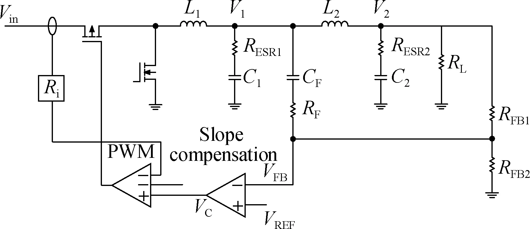
To improve the DC regulation and loop stability, this study proposes a hybrid feedback control method (see Fig.2). The hybrid feedback control method not only guarantees DC regulation with the remote feedback method but also improves loop stability and dynamic response performance by adding high-frequency feedback pathsCFandRF.

Fig.2 Buck with secondary filter and hybrid feedback
1.2 Small-signal analysis
In this study, a small-signal model of the secondary filter of the buck converter is derived on the basis of the peak current mode buck converter to analyze the influence of the hybrid feedback method on stability and to design a high-frequency feedback path. The control loop diagram is shown in Fig.3.GF1is the high-frequency feedback path transfer function from local outputV1toVFB.GF2is the low-frequency feedback path transfer function from remote outputV2toVFB.Gv1dandGv2dare the transfer functions of the output voltagesV1andV2to the duty cycle, respectively.

Fig.3 Small-signal model of peak current mode buck converter with secondary filter and hybrid feedback
The output impedanceZ1ofV1is
(1)
The output impedanceZ2ofV2is
(2)
The transfer function of local outputV1to the inductor current is
(3)
The transfer function of remote outputV2to the inductor current is
(4)
The transfer function of the inductor current to the duty cycle is
(5)
The transfer functions of the output voltagesV1andV2to the duty cycle are given, respectively, as
(6)
(7)
The transfer function of the current inner loop is
(8)
Thus, the transfer functions of the output voltagesV1andV2to the control nodeVCcan be respectively derived as
(9)
(10)
whereGv1candGv2care the control-to-output (V1andV2, respectively) transfer functions.
Therefore, the loop gain is
(11)
Here,GCVis the error amplifier compensator transfer function, andKis the ratio ofGV1CandGV2C.
GFB=GF2+GF1K
(13)
(14)
(15)
(16)
(17)
The feedback transfer functionGFBhas one conjugate zero pairfZ, and the control transferGv2chas one conjugate pole pairfP, as shown in the following equations:
(18)
(19)
The conjugate zero pair is made to cancel the conjugate pol part to reduce the impact on the loop control.RFcan be expressed as
(20)
Fig.4 shows the gain and phase ofGFB. If the value ofCFis too small, then the zero pair inGFBmoves to the right half plane, thus causing a 180° phase delay and instability. To keep the zero-point pair on the left half plane, the following requirement needs to be met:
(21)
Fig.5 shows the gain and phase of the loop gainT. If the value ofCFis too small, then the zero pair inGFBmoves to the right half plane, thereby causing a 180° phase delay and instability.
2 Buck Converter with AVP Control
To reduce the fluctuation of the output voltage when the load jumps, this study proposes a low-cost and easy-to-implement AVP control method (see Fig.6). By adding a load line resistor between the output voltage feedback nodeVFBand the output of the error amplifier, the low-frequency gain of the loop is reduced to increase
the load regulation of the output voltage and thereby optimize the dynamic response of the output voltage.
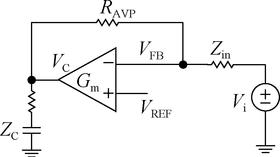
The AVP control method is analyzed using a small-signal model that obtains the loop transfer function and its influence on loop stability. AVP control differs from the conventional control loop in terms of the error amplifier. In this work, the equivalent circuit is altered to facilitate the analysis(see Fig.7).

Fig.7 Equivalent control diagram of error amplifier with AVP
The following formulas can be obtained by analyzing the virtual short and virtual break of the amplifier.
(22)
(23)
Here,Zinis the equivalent input impedance of the amplifier.
(24)
The input to the control transfer function of the error amplifier can be derived as
(25)
(26)
Eq.(26) is substituted into Eq. (25), and the output to the control transfer function is
(27)
The loop gain of the AVP buck converter is
(28)
whereGVCis the control for the output transfer function given as
(29)
From the perspective of amplitude frequency characteristics (see Fig.8), the control loop transfer function only reduces the low-frequency gain without affecting the loop bandwidth. Similarly, the phase frequency characteristics only change the low-frequency phase without affecting the phase margin of the loop. It facilitates the design of the compensator without increasing the complexity of the control loop and the system cost.
The selection of the value ofRAVPis discussed herein. Assuming that the system requires ΔVO_MAXas the output voltage accuracy specification, the output deviation ΔVO_TRis caused by the dynamic load withoutRAVP. The load regulation changes ΔVO_LRcaused byRAVPcan be obtained by
ΔVO_MAX=ΔVO_TR-ΔVO_LR
(30)
The closed-loop output impedance is
(31)
The low frequency gain of the loop gain is
(32)
The load regulation can be calculated by
(33)
Thus, the value ofRAVPcan be derived as
(34)
3 Experimental Results
The prototype is based on a 10 A, 8 MHz buck converter with a secondary filter and AVP control for experimental analysis. The prototype specifications are listed in Tab.1.

Tab.1 Prototype specifications
The results of the noise spectral density are shown in Fig.9(a), and the integrated noise of the specific frequency range can be obtained accordingly. The output noise can be suppressed, especially when the frequency exceeds 1 MHz, that is sensitive for the downstream devices. Fig.9(b) shows a 30 mV peak-to-peak output ripple without the secondary filter and a small 1.7 mV peak-to-peak output ripple with the secondary filter.
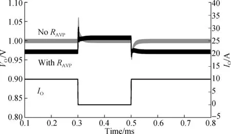
The comparison of the dynamic response results demonstrates that AVP control effectively improves the output voltage dynamic response (see Fig.10). The experimental results show that load regulation increases by 3%, but the output deviation caused by the load step improves by 2%. Therefore, the output voltage accuracy (static and dynamic) meets the 5% accuracy requirement of downstream devices. In other words, the buck converter requires minimal output capacitance and therefore reduces system cost.

Fig.10 Comparison of load transient with and without RAVP
4 Conclusions
1) Current electronic systems have increased requirements for the accuracy and noise of the output voltage of the power supply. Hence, this study proposes a buck converter architecture on the basis of a secondary filter and AVP control.
2) Small-signal models are proposed for the two control methods. The hybrid feedback control and AVP control parameter values are derived accordingly for loop stability analysis.
3) The calculation and experimental results of the buck converter verify the effectiveness of the proposed control method. Moreover, the experimental results show that the noise of the output voltage can be reduced obviously, especially when the frequency is greater than 1 MHz. The dynamic response of the output voltage can be improved by 2%, which meets the required 5% accuracy for the power supply in most mainstream electronic systems.
杂志排行
Journal of Southeast University(English Edition)的其它文章
- Crossed products for Hopf group-algebras
- Concept and evaluation method of equipment system of systems contribution rate
- Comparative study of low NOx combustion optimization of a coal-fired utility boiler based on OBLPSO and GOBLPSO
- Sustainability of health information exchange platform based on information cooperation
- TOD typology: A review of research achievements
- Performance analysis of a novel tobacco-curing system with a solar-assisted heat pump
