Protection of isolated and active regions in AlGaN/GaN HEMTs using selective laser annealing∗
2021-09-28MingchenHou侯明辰GangXie谢刚QingGuo郭清andKuangSheng盛况
Mingchen Hou(侯明辰),Gang Xie(谢刚),†,Qing Guo(郭清),and Kuang Sheng(盛况)
1College of Electrical Engineering,Zhejiang University,Hangzhou 310027,China
2Hangzhou Innovation Center,Zhejiang University,Hangzhou 310027,China
3Ningbo Chipex Semiconductor Co.,LTD.,Ningbo 315000,China
Keywords:gallium nitride,ohmic contacts,laser annealing
1.Introduction
AlGaN/GaN high-electron-mobility transistors(HEMTs)have already emerged as high-performance devices for highpower and high-frequency applications due to the wide bandgap,high-mobility two-dimensional(2D)electron gas(2DEG),high saturation velocity.[1]In order to reduce the production cost,complementary metal–oxide semiconductor(CMOS)-compatible processes manufactured using existing silicon-device fabrication lines are expected.However,standard GaN devices are fabricated using Au-based technologies,such as ohmic contacts.It will bring contamination into the standard Si fabs.Thus,Au-free ohmic contacts are required in CMOS-compatible processes.
However,it is difficult to achieve good ohmic contacts without Au.It is found that Au will enable the formation of TiN spikes.The TiN spikes penetrate the AlGaN layer and direct contact the 2DEG.They create preferential paths for the current.Thus,it is easier to realize low contact resistance.[2]On the contrary,TiN spikes are not found in the Au-free ohmic contacts.[3]Thus,higher annealing temperature is required to form high quality of Au-free ohmic contacts.[3–5]
One promising method to reduce annealing temperature is recessed ohmic contacts.Pre-ohmic recess etching of the Al-GaN barrier has been demonstrated to be an effective method to achieve low resistance and smooth surface morphology of Au-free ohmic contact with a low annealing temperature in un-doped GaN-based HEMTs.[6–9]However,the general fabrication method has not been established.This can be seen from the results that the optimal etching depth varies in the literature,such as partial etching of barrier layer[7]and full removal of barrier layer.[8]The current transport mechanism of recessed ohmic contacts is also not well understood.
With the development of semiconductor manufacturing technology,conventional rapid thermal annealing(RTA)process is facing new problems and challenges.Not only the ohmic contact region,but also the active region and the isolated region suffer from such hightemperature annealing,shown in Fig.1.High-temperature annealing has been reported as the primary cause for the formation of nitrogen deficiency and oxidation of bare(Al)GaN surface,resulting in high density of surface states.These surface states will lead to the degradation of dynamic on-resistance(Ron).[10]Moreover,ion implantation in the isolated region is also not able to withstand such high-temperature annealing.The implantation induced disorders will be recovered under high-temperature annealing.It will cause the failure of isolation.[11–14]
In our previous work,a new ohmic contact formation process for AlGaN/GaN HEMTs based on pulsed laser annealing was reported.[15]The laser can pass through the regions without metal due to the larger energy band gap of GaN(3.4 eV)and SiC(3.25 eV)than the photon energy of the laser with a wavelength of 527 nm(2.36 eV).While the ohmic contact metal can absorb the laser energy and gain annealing effect.Therefore,it is a promising process to protect the active region and the isolated region from high-temperature annealing.
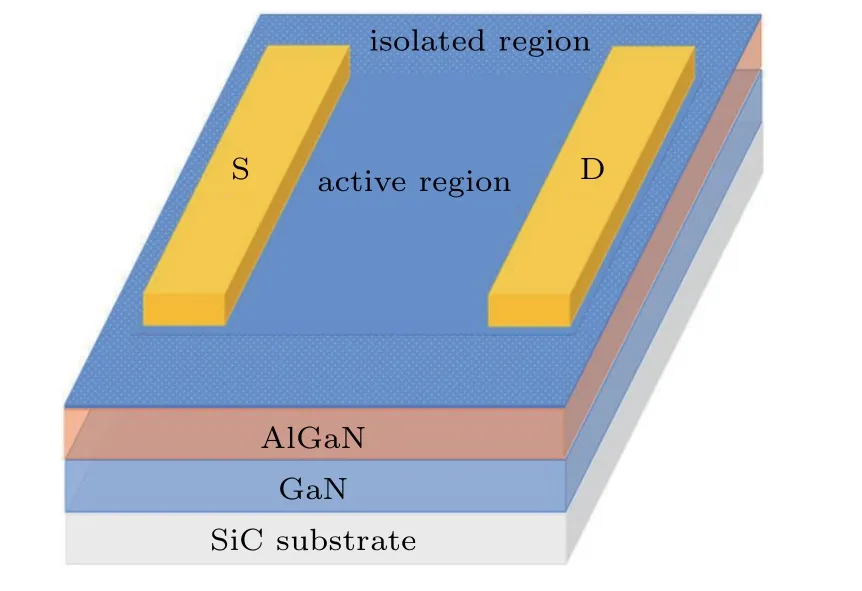
Fig.1.Three-dimensional schematic diagrams of the active region and the isolated region in the AlGaN/GaN HEMTs.
In this letter,AlGaN/GaN HEMTs with Au-free ohmic contacts are fabricated by selective laser annealing(SLA)and RTA.The current transport mechanism of ohmic contacts is investigated.High-temperature annealing are avoided in the active region and the isolated region by SLA.The morphology of AlGaN surface is measured by Atomic force microscope(AFM).No noticeable change of the AlGaN surface morphology confirms the protection of active region and isolated region by SLA.The lower density of surface states in SLA devices is confirmed by the experimental results of capacitance–voltage(C–V)characteristics.As a result,isolation leakage current and dynamic Ronof the SLA devices are improved at the same time.
2.Device fabrication
The 4-inch(1 inch=2.54 cm)epi-wafer used in this paper is provided by NTT Corporation.The schematic crosssectional view of the AlGaN/GaN HEMT is shown in Fig.2.The heterostructure consists of 2-nm GaN cap layer,20-nm Al0.23Ga0.77N barrier layer,300-nm UID GaN channel layer,and 1.8-µm carbon-doped GaN buffer layer.Electron mobility and sheet carrier concentration values of 1350 cm2·V−1·s−1,and 1.05×1013cm−2are measured through Hall effect measurement.The sheet resistance is 439.1Ω/square.First,the ohmic contact areas are recessed by inductively coupled plasma.The etching depth of each sample is varied by changing the etching duration time.Etching depths are measured using AFM.Then,the metal stacks of Ti/Al/Ni/W are successively deposited by sputter.Subsequently,the samples are subjected to nitrogen ion implantation.Then,the ohmic contacts are annealed by SLA and RTA.A laser with a wavelength of 527 nm,300 ns of a pulse duration,5 kHz of pulse frequency,and energy density of 3.5 J/cm2is used.The spot size is 3 mm×0.1 mm.The scan speed is 100 mm/s.The reference sample is annealed by RTA at 850°C–1200°C for 30 s in N2ambient.Next,an Au-free gate metal stacks of Ni/W are deposited.Finally,a 100-nm of SiNxlayer is passivated using PECVD.The electrical characteristics of these devices are measured with Keysight 1505A semiconductor parameter analyzer.
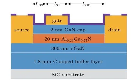
Fig.2.Schematic cross-section of AlGaN/GaN HEMT,where LGS,LG,and LGD(2µm,5.5µm,13µm)are the gate–source distance,gate length,and gate–drain distance,respectively.
3.Results and discussion
3.1.Ohmic contact
Au-based contacts are obtained by electron beam evaporation of Ti/Al/Ni/Au(20/140/50/50 nm).Au-free contacts are obtained by sputtering of Ti/Al/Ni/W(20/140/50/50 nm).The contact resistance(RC)of Au-based contacts and Au-free contacts versus annealing temperature is shown in Fig.3.The Au-based contacts and the Au-free contacts exhibit best ohmic behavior when annealed at 860°C for 30 s and 1100°C for 30 s,respectively.

Fig.3.Contact resistance of(a)Au-based contacts and(b)Au-free contacts versus annealing temperature.
The specific contact resistance(ρC)of Au-based contacts and Au-free contacts versus measurement temperature are plotted in Fig.4.The experimental data of Au-based contacts are fitted by the function:ρC~Tα,withα=1.38.This dependence suggests a“metal-like”behavior due to the formation of TiN spikes.The TiN spikes penetrate the AlGaN layer and direct contact the 2DEG.They create preferential paths for the current.Thus,it is easier to realize low contact resistance with a low annealing temperature.The experimental data of Au-free contacts are fitted by the Thermionic Field Emission(TFE)model.Accordingly,theρCis expressed as[16]

where E0is related to E00by

The characteristic energy E00is defined by

where m∗is the tunneling effective mass,φBis the barrier height,NDis the carrier concentration,and C1is a function of ND,T,andφB.The values ofφB=0.9 eV and ND=3.9×1019cm−3are extracted.During the high-temperature annealing,Ti absorbs nitrogen from the AlGaN layer which results in the creation of nitrogen vacancies within the AlGaN layer.These vacancies in turn play the role of n-type dopants.Thus,higher annealing temperature is required to create abundant nitrogen vacancies.
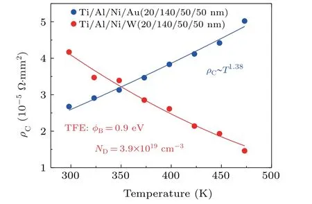
Fig.4.Specific contact resistance of Au-based contacts and Au-free contacts versus measurement temperatures.
In order to reduce annealing temperature,recessed ohmic contact is a promising method.Figure 5 shows the RCof Aufree contacts annealed at 900°C for 30 s versus etching depth.The lowest RCof 0.91Ω·mm is obtained when the etching depth is 20 nm.
For further investigating the current transport mechanism of recessed ohmic contacts,the temperature dependence ofρCfor the recessed ohmic contacts is studied in Fig.6.The experimental data are fitted by the TFE model.The values of φBand NDare extracted.TheφBof recessed ohmic contacts is lower than the non-recessed ohmic contacts.Because when the AlGaN layer is too thin or completely removed,2DEG beneath the contact areas disappeared.Electrons pass horizontally through the recessed side wall of GaN instead of AlGaN which has larger band gap.Thus,as theφBis decreased,the annealing temperature is reduced.

Fig.5.Contact resistance of Au-free contacts annealed at 900 °C for 30 s versus etching depth.

Fig.6.Specific contact resistance of various etching depths versus measurement temperatures.

Fig.7.Specific contact resistance of non-recessed ohmic contacts annealed by SLA versus measurement temperatures.
Figure 7 shows the temperature dependence ofρCfor the non-recessed ohmic contacts annealed by SLA.The experimental data are fitted by the TFE model.The values of φB=1.05 eV and ND=4.1×1019cm−3are extracted.They are similar with the values of non-recessed ohmic contacts annealed by RTA in Fig.4.However,only the ohmic contact region suffers from high temperature process during the SLA.So,the recessed ohmic contacts are not necessary for the SLA.
3.2.Ion implantation isolation
Ion implantation has been widely used for isolation.It can maintain the planarity of the device compared with mesa isolation.SiNxor SiO2as the implanted mask has an advantage over photoresist because of the better thermostability during the ion implantation.However,BOE or HF used to remove the implanted mask will react with the deposited metal.So,the ion implantation is expected to employ before metal deposition.But ion implantation is not able to withstand the high annealing temperature beyond 600°C.Thus,the impact of the SLA and RTA on the ion implantation isolation is studied.
The SRIM software is used to simulate the implantation profile.Multiple energies of 40,80,and 150 keV with doses of 1×1013,2×1013,and 5×1013cm−2are selected for implantisolation.Figure 8 shows the simulated distribution of ion concentrations and vacancies created by the nitrogen ion implantation.With these multiple energy and dose implantations,a uniform vacancy density of 1021cm−3is created across a region of 0.44-µm depth.

Fig.8.Simulated depth profiles of(a)ion concentrations(copc.)and(b)vacancies after N ion implantation.
In order to investigate the impact of SLA and RTA on the isolation leakage current,SLA and RTA are employed before and after ion implantation,respectively.Figure 9(a)shows the isolation leakage current of the devices with SLA employed before and after isolation,respectively.All the SLA devices exhibit low isolation leakage current(about 10−6mA/mm)even at 1000-V stress.It means that the electrical characteristic of the isolated region is not affected by SLA.However,in Fig.9(b),the isolation leakage current increases to 200 mA/mm at 12 V for the devices with RTA employed after isolation.It demonstrates that the high-temperature annealing will recover the implantation induced disorders.Thus,it leads to the failure of isolation.

Fig.9.(a)Isolation leakage current of the devices with SLA employed before and after isolation.(b)Isolation leakage current of the devices with RTA and SLA employed after isolation.
3.3.AlGaN surface state
Figure 10 shows AFM images of the AlGaN surfaces without annealing,with SLA,and with RTA.The scan area is 10µm×10µm.As shown in Fig.10(a),wavy steps and atomically flat terraces are clearly observed on the initial Al-GaN surface.[17]Small root-mean-square(RMS)roughness value of 0.304 nm is obtained from the initial AlGaN surface.In Fig.10(b),no noticeable change of the AlGaN surface morphology is found.The slight increase of RMS roughness value(1.58 nm)may be caused by the contamination introduced during fabrication.In contrast,the RMS roughness value(17.1 nm)markedly increases after RTA,as shown in Fig.10(c).

Fig.10.AFM images of the AlGaN surfaces(a)without annealing,(b)with SLA,and(c)with RTA.The root-mean-square(RMS)value is 0.304 nm,1.58 nm,and 17.1 nm.The scan area is 10µm×10µm.
In our previous work,XPS analysis shows the Al–O peak intensity and Ga–O peak intensity significantly increase after RTA due to the oxidation of AlGaN surface,shown in Fig.11.[10]The oxide grains on AlGaN surface lead to the increase of RMS roughness.Similar result was reported in other literature.[18]

Fig.11.XPS core-level spectra of AlGaN surface before and after RTA.
Figures 12(a)and 12(b)exhibit the C–V curves of the AlGaN/GaN Schottky gate structure at the measurement frequency of 100 kHz.The C–V curves show a two-step capacitance change due to the two interfaces of the AlGaN/GaN Schottky gate structure.[19,20]The nearly flat capacitance around zero bias indicates that the two-dimensional electron gas accumulates at the AlGaN/GaN interface.When the gate bias nears the threshold voltage in the negative bias range,the depletion of the two-dimensional electron gas leads to the decrease of capacitance.When the gate bias increases in the positive bias range,electrons start to distribute in the AlGaN layer,leading to the increase of capacitance.Compared with the SLA devices,the on-set voltage(Von-set)of the RTA devices shifts toward the positive direction.The oxidation of the AlGaN surface during RTA causes severe acceptor-like surface states at the AlGaN surface.The higher density of the acceptor-like surface states leads to the positive shift of Von-set.[21]They also lead to stretch-out phenomenon in the negative bias range.[22]Figures 12(c)and 12(d)compare the frequency dispersion of the C–V characteristics between the SLA devices and the RTA devices.The measurement frequencies are 1 kHz,2 kHz,5 kHz,10 kHz,20 kHz,50 kHz,and 100 kHz.In the positive bias range,the frequency dispersion is observed for both devices caused by the electron capture and emission at the AlGaN surface states.The Von-set shift(ΔV)of 0.3 V in the RTA devices is larger than theΔV of 0.17 V in the SLA devices.The smaller frequency dispersion confirms the lower density of the surface states in the SLA devices.
In order to further investigate the impact of surface states on the dynamic performance of device,characterization of dynamic Ronis carried out by on-wafer measurements.Dynamic Ronwith various off-state VGSis measured in this work.The gate voltage is switched from off-state(below the threshold voltage)to on-state(VGS=0 V),as shown in Fig.13(a).While the drain voltage remains a low voltage(VDS=1 V)in order to suppress the impact of drain voltage on dynamic Ron.The first data is measured at 200µs after the switching from off-state to on-state.Figure 13(b)shows the normalized dynamic Ronwith various off-state VGS.The SLA devices exhibit a low dynamic Ron(1.09 times)after−30-V gate bias stress.However,dynamic Ronof the RTA devices surges up from−15-V gate bias stress,and reaches 65.3 times after−30-V gate bias stress.It demonstrates that the dynamic Ronis effectively suppressed in the SLA devices,owing to reduction of surface states by protecting the bare AlGaN layer from directly exposing under high temperature ambient.

Fig.12.The C–V curves of AlGaN/GaN Schottky gate structure of(a)the SLA and(b)the RTA devices at the measurement frequency of 100 kHz,respectively.Frequency dispersion of(c)the SLA and(d)the RTA devices at the second rising slope in the C–V characteristics.
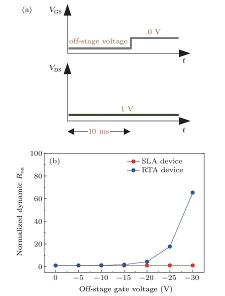
Fig.13.(a)Schematic waveforms of the dynamic Ron measurement.(b)Normalized dynamic Ron with various off-state VGS of the SLA and RTA devices.
4.Conclusion
The SLA and RTA were used in Au-free ohmic contact formation process for AlGaN/GaN HEMTs.The current transport mechanism of ohmic contacts was investigated.Due to the protection of the isolated region and the active region by SLA,the isolation leakage current was maintained about 10−6mA/mm at even 1000-V stress.No noticeable change of the AlGaN surface morphology was found by AFM.The smaller frequency dispersion of C–V characteristics confirmed the lower density of surface states in the SLA devices.Thus,the dynamic Ronwas effectively suppressed.
Acknowledgment
The authors would like to thank Shanghai Micro Electronics Equipment(Group)Co.,Ltd.for their technical support.
猜你喜欢
——全省各级审计机关集中收听收看党的二十大开幕盛况
杂志排行

Chinese Physics B的其它文章
- Origin of anomalous enhancement of the absorption coefficient in a PN junction∗
- First-principles study of plasmons in doped graphene nanostructures∗
- Probing thermal properties of vanadium dioxide thin films by time-domain thermoreflectance without metal film∗
- An improved model of damage depth of shock-melted metal in microspall under triangular wave loading∗
- Signal-to-noise ratio of Raman signal measured by multichannel detectors∗
- Molecular dynamics study of coupled layer thickness and strain rate effect on tensile behaviors of Ti/Ni multilayered nanowires∗