Molecular dynamics study of coupled layer thickness and strain rate effect on tensile behaviors of Ti/Ni multilayered nanowires∗
2021-09-28MengJiaSu宿梦嘉QiongDeng邓琼LanTingLiu刘兰亭LianYangChen陈连阳MengLongSu宿梦龙andMinRongAn安敏荣
Meng-Jia Su(宿梦嘉),Qiong Deng(邓琼),†,Lan-Ting Liu(刘兰亭),Lian-Yang Chen(陈连阳),Meng-Long Su(宿梦龙),and Min-Rong An(安敏荣)
1Fundamental Science on Aircraft Structural Mechanics and Strength Laboratory,Northwestern Polytechnical University,Xi’an 710072,China
2School of Aeronautics,Northwestern Polytechnical University,Xi’an 710072,China
31001 Factory of the Chinese People’s Liberation Army,Xi’an 710119,China
4College of Materials Science and Engineering,Xi’an Shiyou University,Xi’an 710065,China
Keywords:molecular dynamics,Ti/Ni multilayered nanowires,coupled layer thickness–strain rate effect,plastic deformation mechanisms
1.Introduction
Recent years,metallic nanowires with novel physical and chemical properties have attracted extensive attention.[1–3]Unlike the bulk materials,one-dimensional(1D)nanowires possess high surface-to-volume ratio,thus possessing the marvelous mechanical properties,such as pseudoelasticity,[4]superplasticity,[5,6]and ultrahigh strength.[7]The designability of metallic nanowires has brought an excellent combination of component properties,and also greatly expanded potential applications of the materials.Moreover,metallic nanowires/nanorods are also ideal tools to explore the mechanical properties of nanomaterials due to the mature synthesis techniques.[1]With the help of electron microscopy and other precision instruments,in-situ and ex-situ testings are employed to probe the mechanical properties of the materials.[8–11]However,there are still many challenges in exploring the mechanical behaviors of the metallic nanowires/nanorods due to limitation in high-accuracy manipulation and measurement at nanoscale.
Molecular dynamics(MD)simulation with applicable potential function is suitable for modeling and predicting the properties of metallic nanowires.[12]Numerous simulation results have demonstrated that mechanical properties of nanowires are not only related to intrinsic factors(chemical component and crystalline orientation),but also distinctly determined by the extrinsic parameters(cross-sectional size,strain rate,and temperature).The size effect is ubiquitous in metallic nanowires,and observed in almost all kinds of metallic nanowires.[13–19]Wu used the MD method to seek for relaxation and tension behaviors of Cu nanowires.They found that the elastic modulus and strength of the nanowire are dependent on the cross-sectional size,and supposed that the size effect is attributed to surface effect.[13]Wang et al.utilized the MD simulation to evaluate the size effect on tensile behavior of Au nanowires,and the diameters were selected from between 3 nm and 6 nm for different Au nanowires.They found Young’s modulus and yield stress of the same-length nanowires decrease with diameter size decreasing.[15]Additionally,Sainath and Choudhary found the variation of crosssectional width did not affect the deformation mechanism of Fe nanowire,but had the marked influence on the strength and plastic properties of the material.[17]As for metallic glass nanowires,the size effect was also discovered in tension and compression simulations.[18]These observations suggest that novel mechanical properties are ascribed to the high fraction of surface atoms in metallic nanowires.The variation of the cross-sectional size leads the stress and energy distribution of the surface atoms to change significantly,which eventually results in distinct size effect of the nanowires.[19]
Apart from size effect,strain rate effect has also been studied by atomistic simulations.Furthermore,the strain rate effect and size effect are usually combined together to reveal the mechanical properties of nanowires.Wang et al.used the MD method to evaluate strain rate effects(1.384×10⁹s−1≤˙ε≤1.384×10¹⁰s−1)on the tensile properties of Ni nanowires with different diameters(3.94,4.95,and 5.99 nm).They found that yield stress decreased rapidly with strain rate increasing at 0.01 K,while the variation of strain rate barely affected the strength of Ni nanowires at other temperatures.Furthermore,they also revealed that the variation of diameter and strain rate has negligible effect on elastic modulus of Ni nanowires.[20]In addition,Chang et al.investigated the tensile behaviors of Ti nanowires,in which the strain rates are chosen to be 108s−1≤˙ε≤1011s−1.They supposed that nucleation and growth of{10¯12}twins dominated the plastic behaviors in the case of˙ε<1010s−1.For the case of˙ε≥1010s−1,the formation of amorphous phase turned into the main plastic mechanism of the nanowires.[21]Ulteriorly,they studied the tensile behaviors of Ti nanowires with different sizes in a range of 108s−1≤˙ε≤1010s−1.They found that the plastic behaviors after the deformation twinning were controlled by the extrinsic strain rate and cross-sectional size,and the critical size to induce transition of the deformation mechanism decreased with the increase of strain rate.[22]Xie et al.[23]used MD method to reveal strain rate and temperature effect on the plastic deformations of Fe nanowires,and found the plastic deformation varied with those factors.And they also found that at the lower strain or higher temperature,the plastic deformation was dominated by the dislocation propagation,while at the high strain rate or lower temperature,the martensitic phase transformation was attributed to the main plastic deformation mechanism.
Metallic multilayered nanowire(MNW)is a special type of 1D material,which is formed by periodically superimposing two or more metals.Metallic MNWs will combine the mechanical properties of their components,the heterogeneous interfaces forming at the junctions of two components will also bring new deformation mechanisms to the nanowires in the meantime.Previous investigations have intuitively suggested that layer thickness(λ)and interface dramatically affect the mechanical properties of the MNWs.[24–28]Yuan and Wu explored the tensile properties of Cu/Ag nanowires with layer thickness changing.For the loading applied perpendicularly to the interface,plastic deformation mechanism varied from interactions between dislocations and interfaces to interfaces rotation with the layer thickness decreasing.[24]An et al.employed MD methods to investigate the layer thickness dependent tensile behaviors of Ti/Al nanowires.Deformation mechanism varied from interface shear to formation of basal/prismatic planes in Ti layer with the layer thickness increasing.[25]In addition,the influence of layer thickness and modulation ratio on the mechanical properties of Ti/Ni MNWs were further investigated in our previous work.Deformation mechanism also transformed from interface shear to different plastic deformation carriers in Ti layer with layer thickness increasing.Stress and potential energy distribution demonstrated that the surface-driven and interface-driven plasticity were two competitive deformation mechanisms with the modulation parameters changing.[26]Extrinsic strain rate is also crucial for plastic deformation mechanisms of the MNWs.Fan et al.studied the strain rate effect on tensile behaviors of Cu/Au nanowires,and found that the plastic deformation at˙ε=3.333×10⁸s−1is dislocation multiplication and deformation twinning,and the main plastic deformation is the amorphization of crystalline phase at˙ε=1.111×10⁹s−1.[27]Liu et al.evaluated strain rate effect on the mechanical behaviors of Ti/Al MNWs.The results indicated that plastic deformation mechanism transformed from the grain reorientation to the generation of amorphous state as the strain rate increased.Through the strain rate sensitivity analysis,the critical strain rate was observed in the simulations.Below the critical strain rate,the plastic behavior was determined by the grain reorientation and phase transformation.Above the critical strain rate,the amorphization turned into the controlling of the tensile behaviors of the Ti/Al nanowires.[28]
As mentioned above,there have been relatively few researches on the mechanical behaviors of multilayered nanowires,but most of them focus only on the single factor(size effect or strain rate effect).However,actual loading process is often carried out under the coupled extrinsic working conditions.Do the mechanical properties of the MNWs change significantly under the disparate layer thicknesses and strain rates?How do these factors jointly affect the plastic deformation mechanisms of the MNWs?These questions promote an in-depth study on the MNWs.The simulation work in this paper is a continuation of our previous study,which aims to systematically obtain the effects of these extrinsic factors on the tensile behaviors of Ti/Ni MNWs.Through MD methods,the coupling effects of layer thickness and strain rate on the mechanical behaviors of isopachous Ti/Ni MNWs are discovered,and a layer thickness–strain rate-dependent mechanism diagram is also presented to summarize the couple effects on the mechanical properties of the nanowires.The observations from the present work are expected to be able to promote theoretical researches and practical applications of Ti/Ni multilayered nanowires.
2.Computational methods
Three typical layer thickness values(1.31,2.34,and 7.17 nm)are chosen and used to investigate the tensile properties of the isopachous Ti/Ni MNWs.Our previous work has discovered different plastic deformation mechanisms of the samples at these representative modulation parameters.[26]The schematic of isopachous Ti/Ni MNW is shown in Fig.1,the total length varies from 5.24 nm to 28.68 nm along the Z direction,and the dimensions in other directions are fixed at 6.49 nm and 6.64 nm,respectively.The Ti(0001)and Ni(111)planes are selected to be perpendicular to the Z direction(loading direction),since the most of atoms are prone to stack along these close-packed planes to gain the minimum energetic state during the vapor deposition.[29]Owing to the different crystalline structures and lattice constants,semi-coherent Ti(0001)/Ni(111)interfaces are formed at the junctions of two phases as shown in the magnified part of Fig.1.
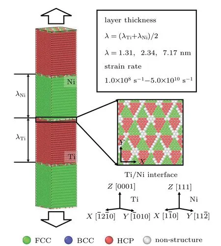
Fig.1.Ti/Ni multilayered nanowire with tension loading applied perpendicularly to the Ti/Ni interface,with insets on right side showing part of interface structure forming at the intersection of two phases,and coordinate systems representing initial orientation of crystalline Ti and Ni,respectively.
Potential function is crucial for the accuracy of MD simulation.In this work,interactions between Ni–Ni,Ni–Ti,and Ti–Ti atoms are depicted by the embedded atom method(EAM).[30,31]This classical EAM potential is wildly utilized to predict the mechanical behaviors of metallic multilayers.[24–28,32,33]The locations and velocities of different atoms are calculated by velocity-Verlet algorithmin time steps of 1 fs.Before loading,samples are first slackened for 30 ps to gain the minimum energetic state.The different strain rates can be obtained by applying various tensile strains per timestep for all atoms,and a wide range of strain rates(1.0×10⁸s−1≤˙ε≤5.0×10¹⁰s−1)is achieved and supplied along the Z direction.During the simulations,the total tensile strain is 0.15 for the most models,while total strain is 0.4 for the case of 5.0×10¹⁰s−1.Period boundary condition is used only in the Z direction,while free boundary conditions are employed in the X and Y directions to calculate the tensile properties of infinite Ti/Ni nanowire.The simulated temperature in this work is selected as 300 K,and Virial theorem[34]is used to calculate the atomic stress of the system as follows:


The common neighbor analysis(CNA)method[35]is used to identify different types of atoms:face-centered cubic(FCC)atom(green),hexagonal close-packed(HCP)atom(red),body-centered cubic(BCC)atom atom(blue),and nonstructured atom(dark gray).After obtaining coordinate information of the simulated atoms,most of the visualization and post-processing procedures are performed by the powerful software-OVITO.[36]
3.Results and discussion
3.1.Tensile properties


Fig.2.Stress–strain curves of isopachous Ti/Ni MNWs with different layer thickness values at various tensile strain rates at(a)λ=1.31 nm,(b)2.34 nm,(c)7.17 nm,(d)Yield stress of all samples at various strain rates.

3.2.Atomic configuration evolutions
The microstructure evolutions of the shortest Ti/Ni MNW(λ=1.31 nm)at a series of strain rates are presented in Fig.3.For the better observation,the microstructures of the nanowire are presented only in the Y–Z plane.The angle,ellipse and rectangle represent interface shear,grain reorientation and amorphization of crystalline structures in the tension process,respectively.At˙ε=1.0×10⁸s−1,the multilayered structure first yields at a tensile strain of 0.025.Plastic behavior is only maintained by the interface at the junction of Ti and Ni crystals.With the successive increase of the applied tension loading,the rotation angle of the interface gradually increases as shown in Fig.3(a).The same phenomena are also observed in the tension process of Cu/Ag[24]and Ti/Al[25]MNWs with a small layer thickness.The phenomenon can be explained as high stress concentration in the interfacial region,while the layer spacing is too small to nucleate dislocations or other defects.Thus,the high local stress is only released by the interface shear.[25]
For the second strain rate,the yield behavior is a combination of interface shear and grain reorientation in Ti layer at a large tensile strain of 0.052.That the new grains rotate into a new orientation is also a way to release the high local stress in the loading process.The disordered structure of the free surface causes new grains to first nucleate from the surface and then release local stress concentration.[25]For the case of ˙ε=5.0×10⁹s−1,figure 3(c)implies that the grain reorientation occurs at a tensile strain of 0.071,some non-structured atoms appear in Ti layer at the large strain.And no obvious plastic deformations are found in the interfacial regions at this time.For the largest strain rate,the formation of amorphous phase turns into a main plastic behavior at the yield strain.As tensile strain increases,the initial Ti layer eventually becomes amorphous state,while some partial dislocations propagate in the Ni layer.
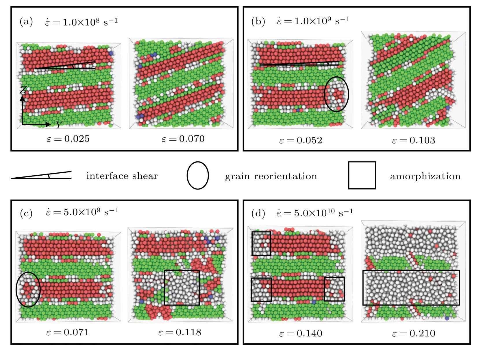
Fig.3.Atomic configuration evolutions of isopachous Ti/Ni MNW withλ=1.31 nm at(a)=1.0×10⁸ s−1,(b)1.0×10⁹ s−1,(c)5.0×10⁹ s−1,(d)5.0×10¹⁰ s−1.The angle,ellipse,and rectangle represent the different plastic deformation carriers in the tension process.
The microstructure evolutions of the intermediate Ti/Ni MNW(λ=2.34 nm)are presented in Fig.4.Unlike the tensile behavior of the shortest nanowire,plastic deformation behaviors at˙ε=1.0×10⁸s−1are the combination of interface shear and grain reorientation in Ti layer as described in Fig.4(a).Going on loading,the completion of grain reorientation and subsequent allotropic phase transformation occurs in“weak”Ti layer,and Ti/Ni interface rotates a larger angle simultaneously.As for the second strain rate,the microstructure evolutions are the same as the former one,and shown in Fig.4(b).For the case of˙ε=5.0×10⁹s−1,the plastic deformation is maintained only by the Ti layer,and no more interface shear can be found in the tensile process.The grain reorientation,growth of the new grains and phase transformation dominate the plastic deformations in the tensile process.As for the case of the largest value of˙ε,the amorphization first germinates at the weaker points in Ti layer and finally occupies the entire Ti layer.Meanwhile,a number of dislocations is observed to have propagated in the Ni layer.
For the case of isopachous Ti/Ni nanowires with larger layer thickness,the plastic behaviors are greatly different from those of previous two samples.The microstructure evolutions of the longest Ti/Ni MNW(λ=7.17 nm)are presented in Fig.5.For the better observation,the surface atoms have been removed away,and the three-dimensional(3D)structures of the Ti/Ni nanowire are presented in the figure.For the first strain rate,the new grain trends to nucleate from free surface and propagates in the upper Ti layer atε=0.021,which is shown by the black ellipse in Fig.5(a).The new grain grows quickly until occupying the entire upper Ti layer.Further increasing the tensile strain,the new grain starts to nucleate and expand quickly in the lower Ti layer atε=0.042.Finally,the upper Ti layer and the lower Ti layer transform to the new orientation completely.As shown in Fig.5(a),the basal plane of parent Ti layer is perpendicular to the basal plane of twin Ti layer,i.e.,initial[0001]axis of the parent phase transforms to[1010]axis of the twin phase.It should be pointed out that grain reorientation presents a twinning-like behavior,which has also been discovered in simulation[21,22,37–39]and experiment[40,41]of HCP materials.Hereafter,the newly formed Ti/Ni nanowire undergoes another elastic stage until the tensile strain reaches the 0.073.As the axis of the newly formed Ti layer is subjected to the tensile loading,the FCC-Ti embryos trend to nucleate from the surface and then grow in the upper Ti layer as indicated by black circles in Fig.5(a).After that,the FCC phase grows and occupies the entire Ti layer as a result of dense basal dislocations’propagation and accumulation of FCC stack faults.[37,38,42]And the specific orientational relationship of grain reorientation and the phase transformation have been described specifically in our previous work.[26]
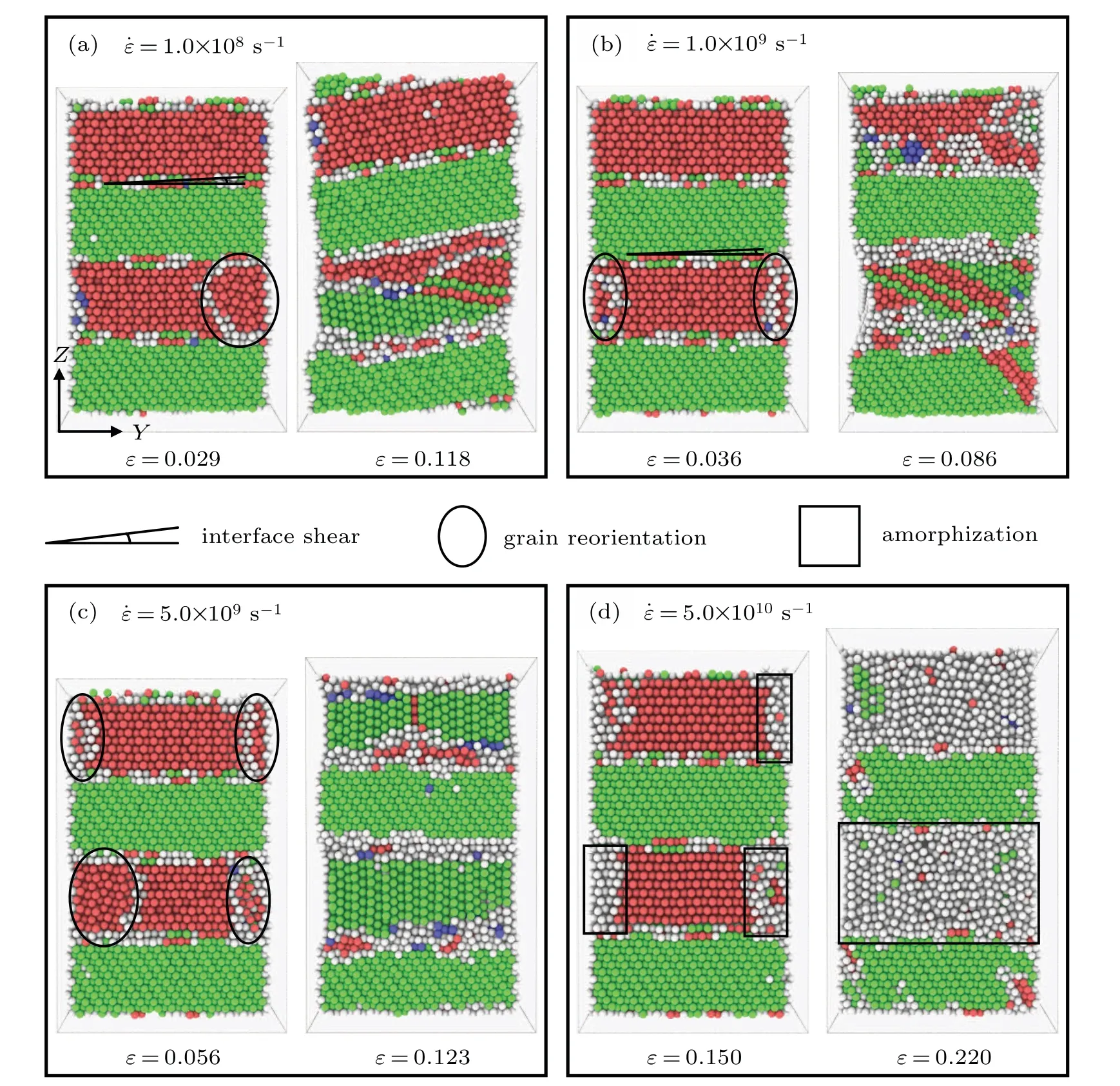
Fig.4.Atomic configuration evolutions of isopachous Ti/Ni MNW withλ=2.34 nm(a)at˙ε=1.0×10⁸ s−1,(b)1.0×10⁹ s−1,(c)5.0×10⁹ s−1,and(d)5.0×10¹⁰ s−1,with angle,ellipse,and rectangle denoting different plastic deformation carriers in the tension process.
At the second strain rate,the plastic deformations are similar to those at˙ε=1.0×10⁸s−1,which contains the grain reorientation,allotropic phase transition and dislocations’movement in Ti layer,while Ni layer provides spring support in the tensile process.In addition,nucleation sites of new grains increase with strain rate increasing for the longest samples at 1.0×10⁸s−1≤˙ε≤5.0×10⁹s−1.Similar results were also discovered in tensile behaviors of Ti nanowires[22]and Ti/Al nanowires,[28]which indicates the surface nucleation sites are positively correlated with the strain rate in the small strain rate region and the intermediate strain rate region.
At˙ε=5.0×10¹⁰s−1,the amorphization is generated first in Ti layer and then grows rapidly until amorphous phase occupies the whole Ti layer,and the plastic deformation in Ni layer is mainly the dislocation motion and amorphization in the local region.It is obvious that the plastic behaviors are sustained mainly by the Ti layer,and the interface seems not to participate in plastic deformation for the longest sample at a lower strain rate.While at a high strain rate(˙ε>1.0×10¹⁰s−1),amorphization of both crystalline Ti layer and Ni layer turns into the main plastic deformation carrier.

Fig.6.Atomic fraction evolutions of different structures of the longest Ti/Ni MNWs at strain rates of(a)1.0×10⁸ s−1,(b)1.0×10⁹ s−1,(c)5.0×10⁹ s−1,and(d)5.0×10¹⁰ s−1.
3.3.Strain rate-dependent tensile behaviors of the longest sample
The microstructure evolution diagram indicates that the plastic behaviors of the longest sample become more complex with the variations of the strain rates.After the grain reorientation,the subsequent plastic behavior presents phase transformation or amorphization in Ti layer,which is determined by the specific strain rate.
Figure 6 depicts the atomic fraction evolutions of different structures at disparate strain rates.The difference value of HCP structure or FCC structure in the tensile process represents the extent to which the phase transition takes place.Similarly,the difference among the non-structure atoms represents the degree of amorphization.In a small strain rate region,the phase transformation is the dominant plastic behavior.As strain rate increases,the fraction of FCC atoms grows markedly,and all the HCP atoms seem to transform into FCC atoms in the intermediate strain rate region.Additionally,the fraction of non-structure atoms is unchanged in the tensile process as shown in Figs.6(a)and 6(b).
Nevertheless,a large fraction of crystalline atoms turns into non-structure atoms in large strain rate region as shown in Fig.6(d).It is revealed that both Ti layer and Ni layer take part in the plastic deformation.In a critical strain rate region,the atomic fractions of both HCP(or FCC)and nonstructure atoms change in the loading process,phase transformation and amorphization jointly dominate the plastic deformation.According to previous studies,the phase transformation is caused by the dense dislocation motion in the HCP crystal,and finally results in the continuous accumulation of FCC stacking faults.[37,38,42]Namely,the dislocations’movement in Ti layer takes place easily in the small strain rate region and the intermediate strain rate region.There is ample time to actuate dislocations propagation along a certain plane at this series of strain rates,so that the high stress of the system is released.Nevertheless,there is not enough time to induce the nucleation of dislocations and other plastic deformation carriers,and crystalline atoms tend to collapse to form amorphous structures,thereby dissipating the local stress concentration rapidly at the high strain rates.[43,44]

Fig.7.Variations of potential energy with strain of the longest Ti/Ni nanowires at various strain rates.
The variation of strain rate affects not only the microstructure evolution of the sample,but also the energy evolution in a tensile process.Strain rate effect on energy evolutions of the longest Ti/Ni MNW is plotted in Fig.7.The energy here refers to the average atomic potential energy,which is the total potential energy divided by the number of atoms.Figure 7 shows that energy-strain curves display different trends with the increasing of the applied strain.Like the stress–strain curves,the first peak energy also indicates the end of the elastic stage and the beginning of the plastic stage.And the peak energy is positively correlated with extrinsic strain rate.A more meaningful parameter to describe the energy evolution during the deformation is the energy barrier,which can be defined as the difference between initial and final energy.In a statistical sense,the energy barrier reflects the minimum energy required for atom to go from one configuration to another.[37,42]In this work,the energy barrier is defined as the difference between the initial value of energy and the first peak value of energy.The parameter here reflects not only the maximum elastic energy stored in the simulated system during deformation,but also the minimum energy required to induce the plastic deformation.Therefore,energy barrier is vital to the assessment of the strain rate effect on the tensile behavior of the Ti/Ni MNWs.Energy barriers of the different samples are also indicated in Fig.7.The values ofΔE1andΔE2are relatively equal,andΔE4is much higher than previous value.As is well known,the potential energy relies just on the relative position of the simulated atoms.For the case of small strain rate,most of atoms have adequate time to reach the lower energetic position,so the system is in a low energy state.Once increasing the strain rates,the number of atoms to reach lower energy position gradually decreases,resulting in the increase of energy barriers finally.When the strain rate is high enough,due to the lack of sufficient time,almost all atoms are in a higher energy state,i.e.,the amorphous state.It seems that ΔE3is a critical energy barrier in the present dissertation,as the amorphous structure trends to expand in the tensile process when the value is larger thanΔE3.
3.4.Layer thickness-dependent tensile behaviors in small strain rate region
The microstructure evolution analysis shows that interface shear for the shortest sample is an interface-driven plastic behavior.While the grain reorientation generated from the free surface is surface-driven plastic behavior.Interface and surface play the vital roles in the tensile behavior of Ti/Ni MNWs.Surface atoms are in higher stress state than the internal atoms due to the lack of neighboring atoms.[13]Likewise,interface atoms are also in high stress state because of misfit dislocations forming at the semi-coherent interface.[26]Thus,plasticity is likely to occur from the interface or free surface.There seems to exist a competition between the interfacedriven plastic deformation and surface-driven plastic deformation in MNWs.Exploring the underlying mechanism,the Ti/Ni nanowire is divided into three parts:Ti/Ni interface,Ti layer,and Ni layer.Here,the interfacial atoms refer to 4 layers of atoms between the HCP crystalline structure and FCC crystalline structure,for they show more complex stress distribution than the internal atoms.More details about interfacial atoms can be found in Ref.[26].Figure 8 depicts the fractions of the interfacial,Ti and Ni atoms for different samples.Although the fraction of surface atoms in Ti layer cannot be displayed intuitively,it is proportional to the atomic fraction of Ti atoms.It can be seen in Fig.8,the atomic fraction of interfacial atoms decreases as the layer thickness increases,whereas the fraction of Ti atoms and the faction of Ni atoms show opposite trends.Interfacial atoms occupy a large fraction of the shortest sample.Therefore,the plastic deformation tends to first occur at the interface,and the interface has sufficient time to complete the interface shear in a small strain rate region.Similarly,the longest sample has a large fraction of Ti atoms,the plastic deformation tends to preferentially arise from the surface,new grains have sufficient time to complete the nucleation and propagation.While for the intermediate sample,the fractions of different atoms are nearly equal,so plastic deformation is a mixture of interface shear and grain reorientation.Consequently,the variation of microstructure parameters will significantly affect the stress distribution,which will cause the transformation driven by deformation mechanism.
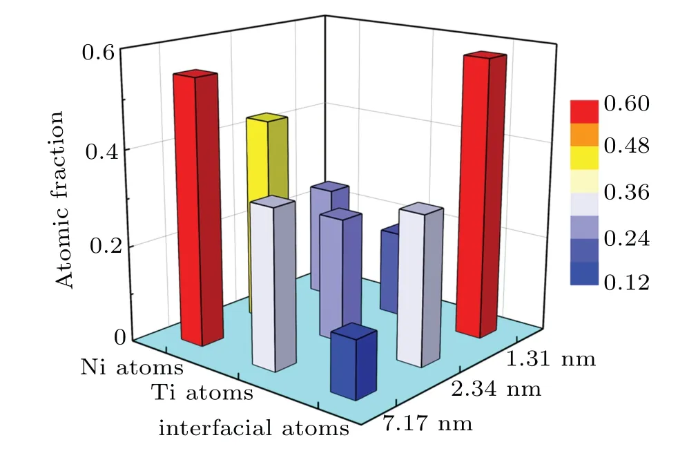
Fig.8.Atomic fractions of different structures for disparate Ti/Ni nanowires.
3.5.Coupling effect of layer thickness and strain rate on tensile properties of isopachous Ti/Ni nanowires
The further analyzing of the coupling effect of layer thickness–strain rate on the strength of isopachous Ti/Ni nanowires reveals the relationship between yield stress and strain rate in double logarithm coordinate as shown in Fig.9,with the inset displaying the yield stress–strain rate relations in Cartesian coordinate.Four strain rate regions are colored in light green,in yellow,in orange,and in pink,respectively.Corresponding plastic deformations are displayed in the inset.To demonstrate the strain rate effect of on tension process intuitively,the strain rate sensitivity(SRS)factor m is used to assess the strain rate effects on the strength of different Ti/Ni nanowires.Combining the previous stress–strain curves and microstructure evolutions,the plastic deformation mechanisms vary in the disparate strain rate regions.Thus,it is necessary to evaluate the SRS values in different strain rate regions.In this subsection,the parameter m is described as formula(2),and relevant values of different models are shown in the right part of the figure,

Fig.9.Variations of logarithmic stress with logarithmic strain rate for isopachous Ti/Ni MNWs,with disparate color blocks marking different plastic deformation carriers,and inset showing yield stress–strain rate relations in Cartesian coordinate.
In the small strain rate region,changing strain rate significantly affects the strength of the shortest sample,while the values of m1of other two samples are less than the value of the shortest sample.In the intermediate strain rate region,the values of m2of all models are higher than those values of m1,and the longest model shows strong strain rate sensitivity.Whereas,changing strain rate greatly affects both the yield stress of the intermediate sample and the yield stress of the longest sample in the large strain rate region.It can be inferred from Fig.9 that the shortest sample shows the stronger strain rate sensitivity in the small strain rate region.For the other strain rate regions,increasing strain rate greatly affects the strengths of large-sized samples.
The plastic deformations of isopachous Ti/Ni nanowires under different layer thickness values and strain rates are summarized in Fig.10.In the small strain rate region and the intermediate strain rate region,increasing the layer thickness causes the main plastic deformations to transform from interface shear to grain reorientation and phase transformation.Further increasing the strain rate,the main plastic deformations of Ti/Ni MNWs changes from interface shear(the shortest sample)or grain reorientation(the longest sample)to the amorphization of crystalline structure for all samples.It should be pointed out that the change of the deformation mechanism for Ti/Ni MNWs is not abrupt.Actually,there are a critical layer thickness of 2.34 nm in the small strain rate region,and a critical strain rate region of 5.0×10⁹s−1≤˙ε<1.0×10¹⁰s−1in the present work.In the criticalcase,the plastic deformation behaviors are the mixture of plastic deformations below and above the critical value.Taken together,these findings suggest that layer thickness and strain rate are key factors to determine the tensile behaviors of Ti/Ni nanowires.The relationship between those factors is not independent but coupled to determine the deformation mechanisms of the nanowires.
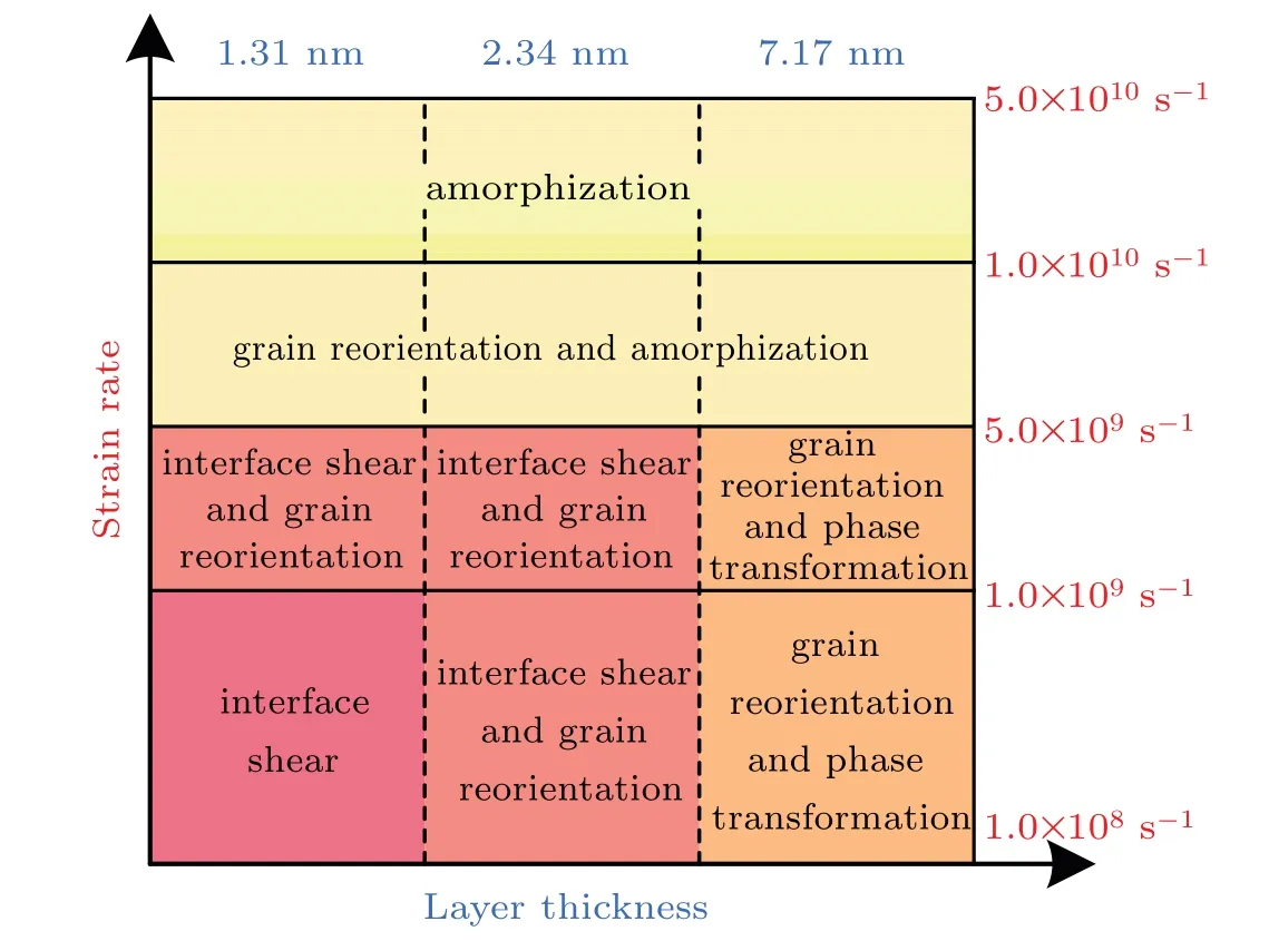
Fig.10.Diagram of layer thickness–strain rate-dependent mechanism of isopachous Ti/Ni MNWs.
3.6.Effect of modulation ratio on tensile properties of unequal Ti/Ni nanowires
It has been demonstrated above that the layer thickness significantly affects the mechanical properties of isopachous Ti/Ni nanowires.Actually,the modulation ratio also plays an important role in the mechanical properties of unequal multilayered materials.[26,45–47]Our previous study has confirmed that tensile properties of unequal Ti/Ni nanowires are dominated by the modulation ratios at a certain strain rate.[26]Thus,more attention is paid to the variation of strain rate affecting the tensile properties of unequal Ti/Ni nanowires in this part.For the unequal Ti/Ni nanowires,thickness of Ti(or Ni)layer is fixed at 2.34 nm,and the thickness of Ni(Ti)layer is 4.68 nm(7.02 nm).Thus,modulation ratios are selected to beη=λTi:λNi=1:3,1:2,2:1,3:1,respectively.The stress–strain curves of unequal samples at various strain rates are plotted in Fig.11,and the curves of isopachous samples(η=1:1)under the same loading conditions are also shown in Fig.11.Like the stress–strain curves of isopachous samples,the wave-like stress–strain relationships with increasing tensile strain can be discovered for all unequal samples when the strain rate is 5.0×10⁸s−1.For the case of˙ε=5.0×10⁹s−1,the stress–strain curves grow steadily with the increase of applied strain,and peak stresses are larger than the values at 5.0×10⁸s−1.When the strain rate reaches 5.0×10¹⁰s−1,no obvious peaks can be found in stress–strain curves for all samples.Figure 11(d)depicts the variation of yield stress with the strain rate for unequal Ti/Ni nanowires.It can be seen that the yield stress first increases with the increase of strain rate,then abruptly drops at 1.0×10¹⁰s−1,and finally increases with the strain rate increasing when the strain rate is larger than 1.0×10¹⁰s−1.The maximum yield stress is obtained at˙ε=5.0×10⁹s−1,which is consistent with the results of isopachous samples.However,when the thickness of Ti layer is fixed,the yield stresses maintain constant values as the strain rate is lower than 1.0×10⁹s−1.Further increasing the strain rate,yield stresses of unequal Ti/Ni nanowires with large Ni layer possess the higher values at a specific strain rate.When the thickness of Ni layer is fixed,the yield stresses first increase with thickness of Ti layer decreasing as the strain rate is below 5.0×10⁹s−1.And for the larger strain rates,the differences between the yield stresses at the specific strain rate are relatively small.The yield stresses with strain rate of all unequal samples vary strongly with the modulation ratio.When the strain rate is lower than 1.0×10⁹s−1,the plastic deformations are sustained by weak Ti layer,and increasing the thickness of Ti layer leads the yield stress to drop.When the strain rate is larger than 1.0×10¹⁰s−1,amorphization turns into the main plastic deformation in both crystalline Ti and Ni layers,increasing the thickness of Ti or Ni layer can promote the probability of local amorphization in crystalline phase.Therefore,the yield stress is positively related to the strain rate in this strain rate region.When the strain rate is 5.0×10⁹s−1,the grain reorientation and amorphization in the local region jointly dominate the plastic deformation mechanisms of unequal samples,and the maximum yield stresses are obtained at this critical strain rate.
However,the variation of the modulation ratio barely changes the deformation mechanism of the unequal Ti/Ni nanowires.Comparing Fig.2 with Fig.11,changing the modulation structure will vary only tensile properties of certain Ti/Ni nanowires.As the monolayer thickness of Ti or Ni in unequal Ti/Ni nanowire is greater than 2.34 nm,the fraction of the crystalline phase is greater than the counterpart of the interfacial structure.Therefore,the plastic deformations are caused mainly by the crystalline phase,which consist of grain reorientation and phase transformation in Ti layer in small and intermediate strain rate region,and the local amorphization of crystalline phase in large strain rate region.
Besides size and strain rate effect,the temperature effect is a significant factor affecting the mechanical properties in most of metallic nanowires.[13,16,20,23,25,28]We use the MD method to evaluate the tensile properties of isopachous Ti/Ni MNWs in a wide range of temperatures(0.01 K–500 K).When the layer thickness and strain rate are fixed,increasing temperature causes only the elastic modulus and yield stress to change,showing obvious thermal softening effect.However,plastic behaviors of the nanowires scarcely change under the same working conditions.This also proves that the extrinsic layer thickness and strain rate are determinant factors to control the tensile behaviors of the nanowires.Furthermore,geometric shape and cross-sectional size also influence the mechanical performance of metallic nanowires due to the change of stress distribution of the surface and internal atoms.However,the cross-sectional shape and size are fixed to ascertain the layer thickness effect on the tensile properties of the nanowires in this work.It is difficult to assess how these factors affect the mechanical performances of the MNWs.Therefore,more efforts are needed to systematically obtain the effects of different factors on tensile behaviors of Ti/Ni nanowires.
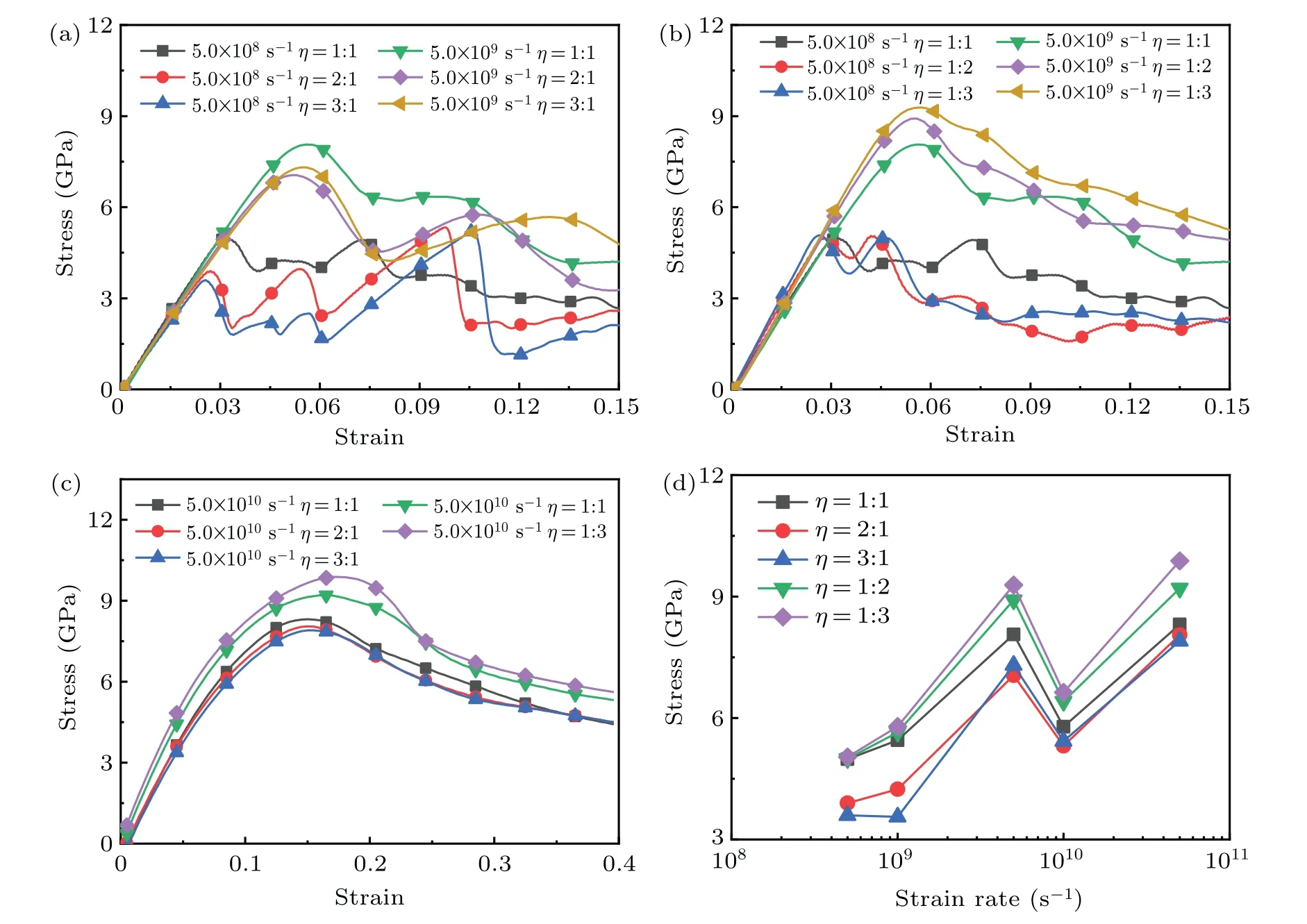
Fig.11.Stress–strain curves of unequal Ti/Ni MNWs at various tensile strain rates.(a)Stress–strain curves of unequal nanowires with different modulation ratios,where layer thickness of Ni layer is fixed at 2.34 nm;(b)stress–strain curves of unequal nanowires with different modulation ratios,where layer thickness of Ti layer is fixed at 2.34 nm;(c)stress–strain curves of all unequal samples at strain rate of 5.0×10¹⁰ s−1;and(d)yield stresses versus strain rate of all unequal samples.
4.Conclusions
We have utilized molecular dynamics method to investigate the tensile behaviors of Ti/Ni MNWs,various modulation parameters and strain rates are selected in this work.The results demonstrate that the coupled layer thickness and strain rate effect significantly affect the tensile behaviors of Ti/Ni MNWs.The main conclusions of this work are as follows:
(i)Yield stresses of all Ti/Ni MNWs exhibit different trends varying with strain rate increasing.The four strain rate regions are observed in the tension process.Yield stresses of all MNWs first increase in the small strain rate region(1.0×10⁸s−1≤˙ε<1.0×10⁹s−1)and intermediate strain rate regions(1.0×10⁹s−1≤˙ε<5.0×10⁹s−1),then decrease in the critical strain rate region(5.0×10⁹s−1≤˙ε<1.0×10¹⁰s−1),and finally increase in the large strain rate region(1.0×10¹⁰s−1≤˙ε≤5.0×10¹⁰s−1).
(ii)Isopachous Ti/Ni MNWs with different values of layer thickness exhibit disparate plastic deformation mechanisms with the strain rate increasing.For the shortest sample(λ=1.31 nm),the initial plastic behavior transforms from interface shear into the amorphization of the crystalline structure.For the intermediate sample(λ=2.34 nm),the initial plastic behavior transforms from the combination of interface shear and grain reorientation into the amorphization of the crystalline structure.For the longest sample(λ=7.17nm),the initial plastic behavior transforms from grain reorientation into the amorphization of the crystalline structures.There exists a critical strain rate region for all samples,the plastic deformation behaviors are the mixture of plastic deformations below and above the criticalvalue.
(iii)The shortest sample shows the stronger strain rate sensitivity in the small strain rate region.While,the variation of strain rate greatly affects the strength of large-sized sample in the large strain rate region.
(iv)Modulation ratio significantly affects the tensile properties of unequal Ti/Ni MNWs,but barely influences the plastic deformation mechanisms of the materials.
猜你喜欢
杂志排行

Chinese Physics B的其它文章
- Origin of anomalous enhancement of the absorption coefficient in a PN junction∗
- Protection of isolated and active regions in AlGaN/GaN HEMTs using selective laser annealing∗
- First-principles study of plasmons in doped graphene nanostructures∗
- Probing thermal properties of vanadium dioxide thin films by time-domain thermoreflectance without metal film∗
- An improved model of damage depth of shock-melted metal in microspall under triangular wave loading∗
- Signal-to-noise ratio of Raman signal measured by multichannel detectors∗