First-principles study of plasmons in doped graphene nanostructures∗
2021-09-28XiaoQinShu舒晓琴XinLuCheng程新路TongLiu刘彤andHongZhang张红
Xiao-Qin Shu(舒晓琴),Xin-Lu Cheng(程新路),Tong Liu(刘彤),and Hong Zhang(张红),†
1College of Mathematics and Physics,Leshan Normal College,Leshan 614000,China
2College of Physics,Sichuan University,Chengdu 610065,China
3School of Science,Xihua University,Chengdu 610065,China
Keywords:doped graphene,absorption spectroscopy,time-dependent density functional theory
1.Introduction
As a one-atom-thick material with extreme light confinement,strong optical response,and broad electronic and optoelectronic tunability,graphene has attracted great attention in the past decade in many fields,such as biological objectives,[1–5]electrocatalysis,[6]DNA sensors,[7]high-resolution transmission electron microscopy(HRTEM),[8]spintronics,[9,10]flexible electronics,[11,12]biocultivation,[13]desalting,[14]electronics,[15–18]photonics,[19]nanoelectronics,[20]biosensors,[21]supercapacitors,[22,23]drug transport,[24,25]hydrogen reservation,[26]transistors,[27]polymer nanocomposites,[28,29]superconductors,[30–32]optical technologies,[33]nanoantenna,[34]and fuel cells.[35]In the terahertz-to-mid-infrared range,graphene plasmons are related to the collective stimulation of free charge carriers and have a higher degree of tunability and mode restriction,and a longer propagation distance than the noble metals’plasmons.[36–40]The carrier plasmon mobility of graphene is reduced to different degrees according to the type and concentration of dopants[41,42]and other defects,[43]especially in the edge structures of nanoscaled ribbons and other nano-geometries.[39]Feasible strategies for the implementation of graphene-based plasmonics in the near-IR-to-visible light range and the relative effects are reported in Ref.[39].
The introduction of B or N atoms into the graphene lattice is the center of extensive scientific research to improve the electronic structure of graphene.[44–51]Substitution of B atoms or N atoms has been predicted to reduce the Fermi level,[48,51,52]resulting in p or n doping just as it is frequently used in current semiconductor technology.A p or n characteristic has recently been confirmed in hanging graphene containing single B dopant or N dopant.[51]Some studies reported the introduction of a band gap into graphene by doping with boron or nitrogen.[46,47]Here in this work discussed are the position and number of doped nitrogen atoms and other types of doping atoms,including boron,aluminum,silicon,phosphorus,and sulfur atoms,and their effects on plasmon excitation of the doped graphene nanostructure.These elements are adjacent to carbon in the periodic table of elements,and the electronegativity of boron,nitrogen,aluminum,silicon,phosphorus,and sulfur are 2.04,3.04,1.61,1.90,2.19,and 2.58,respectively,close to the electronegativity of carbon(2.55).Collective stimulations of N/B-doped graphene nanostructures have been addressed in various studies.However,to the best of our knowledge,the collective stimulations of aluminum/silicon/phosphorus/sulfur-doped graphene nanostructures are investigated herein for the first time.
2.Computational studies
Plasmons in doped graphene nanostructures are studied by time-dependent density functional theory(TDDFT).[53]Collective stimulations are investigated mainly in the orientation parallel to the plane of the doped graphene nanostructures.The danglingσ-bonds at the edges are saturated by hydrogen atoms.The effects of different positions and numbers of nitrogen dopants are investigated,and the influence of different doping atoms is discussed.Computations are carried out by employing real-space TDDFT code OCTOPUS,[54]where C,H,N,B,S,Al,and Si atoms are represented by Troullier–Martins pseudopotentials.[55]The local-density approximation(LDA)for exchange–correlation potentials is applied to both ground and excited state computations.[56]
The linear optical absorption of the system is obtained by the program developed by Yabana and Bertsch,[57]where all frequencies of the system are stimulated by providing diminutive value momenta(κ)for the electrons.The frequencies of the system are obtained by converting the ground-state wave functions through the following equation:
and then these resulting wave functions are spreaded.
Then,the spectrum is acquired according to the dipole intensity function S(ω)expressed as
where the dynamical polarizability(α(ω))is essentially the same as the Fourier transform of the dipole moment of the system d(t)expressed as
Employing this boundary value,the Thomas–Reiche–Kuhn f-sum rule can be used to obtain the number of electrons(N)from the following equation:

This program has been applied to a number of examples,successfully generating reliable absorption spectra.The stimulation region is delimited by allocating a sphere centered on each atom,with a radius of 6˚A and the same mesh grid of 0.3˚A.In real-time spreading,a Kohn–Sham wave function is developed for normally 6000 paces of a time pace of 0.003¯h/eV or 0.00198 fs.
For XG(doped graphene with doping atom X,named XG,X=B,N,Al,S,Si,P;G=graphene),the total densities of states(TDOSs)and partial densities of states(PDOSs)are simulated in the context of the ab initio density functional theory(DFT)by using the Dmol3 package.[58]During calculations,the plane wave in the generalized gradient approximation(GGA),expressed by the Perdew–Burke–Ernzerhof(PBE)functional,[59]is employed.
3.Results and discussion
Cartesian coordinates are employed to place the atoms in the xy plane.The zigzag edge is set to be parallel to the y axis,while the armchair edge is oriented perpendicularly.However,this study focuses primarily on plasmonic stimulation in the orientation parallel to the plane of the doped graphene nanostructure.The effects of different positions and numbers of nitrogen dopants in N-doped graphene are discussed,and the influence of different doping atoms is analyzed.The N-doped graphene with doping position,n,is named n#N-doped system correspondingly(n=1,2,3,4,5,6),while N-doped graphene nanostructure with the number of nitrogen atoms,n,is denoted as nN-doped system correspondingly(n=1,2,3,4,5,6).Doped graphene with doping atom,X,is named XG system correspondingly(X=B,N,Al,Si,P,S).The induced charge plane is parallel to the plane of the doped graphene nanostructure,and the perpendicular space between the plane of the doped graphene nanostructure and the plane of the induced charge density is computed to be 0.9˚A.
The influence of the distance between the two layers and the number of layers of nitrogendoped graphene were studied in our previous work.[60]
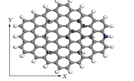
Fig.1.Structure of a single layer of hexagonal nitrogen-doped graphene.The nanostructure is approximately 1.8 nm in size and contains 79 carbon atoms(gray spheres),22 hydrogen atoms(white spheres),and one nitrogen atom(blue sphere).The positions of the nitrogen atoms are marked in the diagram.
In this study,nitrogen doping is realized as indicated Fig.1.The doping concentration is 1.25%.Two electrons are provided by graphitic N to form aπ-bond with the shape of vacant orbitals.The number of delocalized electrons decreases in comparison with those of undoped graphene.Compared Figs.2(a)and 2(c)with Figs.2(b)and 2(d),the intensity of the pulse stimulation polarized in zigzag-edge orientation(y axis)is slightly lower than that of the pulse stimulation polarized in armchair-edge orientation(x axis).The pulse stimulation polarized in armchair-edge orientation(x axis)reduces the intensity of the optical absorption of the 1#,3#,2#,4#,5#,and 6#N-doped system and red-shifts the spectral line of the 4#,3#,5#,1#,6#,and 2#N-doped system adjacent to energy resonance dots at 5 eV.The pulse stimulation polarized in the zigzagedge orientation(y axis)reduces the intensity of the absorption spectrum of the 3#,1#,6#,2#,5#,and 4#N-doped system and red-shifts the spectral line of the 4#,6#,3#,5#,1#,and 2#N-doped system adjacent to the energy resonance dot at 5 eV.The introduced nitrogen atom destroys the symmetry of the graphene nanostructure.A higher degree of symmetry destruction is correlated with weaker optical absorption.Even more interestingly,the optical absorption is split into two parts adjacent to energy resonance dot at 5 eV for the doping positions 3#,4#,and 5#by pulse stimulation polarized in armchair-edge orientation(x axis).
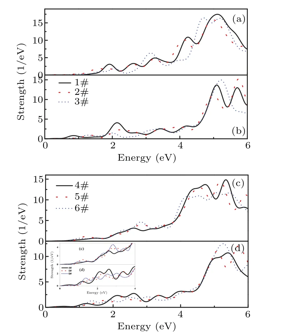
Fig.2.Dipole response(optical absorption)of n#N-doped graphene nanostructures obtained by pulse stimulation polarized in((a),(c)x-axis and((b),(d))y-axis directions.
To clarify the principle of the vibration behavior,we discuss the spatial dependence of the induced charge response on the vibration frequency.The low-energy resonances are located in the border zone.The induced charge density distributions at these plasmon resonance points have dipole characteristics.The pulse stimulation polarized in armchair-edge direction(x axis)results in the scattering of the induced charges of most resonance dots along the zigzag-edge(y axis)direction as shown in Fig.3(c),while the pulse stimulation polarized in zigzag-edge(y axis)direction results in the scattering of the induced charges of most resonance dots along the armchair-edge(x axis)direction as presented in Figs.3(a),3(b),and 3(d).In addition,we believe that the lower-energy plasmon is a longrange charge transfer plasmon(CTP)mode due to the electron motion along the direction where the electrons can move over a longer distance.Figure 3 presents the Fourier transform of the induced charge density for a hexagonal N-doped graphene nanostructure with different nitrogen-doping positions,i.e.,1#N-doped system(Fig.3(a)),3#N-doped system(Fig.3(b)and 5#N-doped system(Figs.3(c)and 3(d).The polarization direction is along the armchair edge at energy resonance dots of 5.18 eV(Fig.3(c)).The polarization orientation is along the zigzag edge at energy resonance dots of 5.10 eV(Fig.3(a)),5.22 eV(Fig.3(b)),and 5.08 eV(Fig.3(d)).The induced charge density profiles of these plasmon resonance points each have a dipole-like character as shown in Fig.3.All the energy resonance dots are the main peaks adjacent to energy resonance dot at 5 eV.The induced charge calculation formula of Fourier transform is
where,ωis the resonance frequency,T is the total time of developing of Kohn–Sham wave function,and t is the time step of 9¯h/eV or 5.94 fs.

Fig.3.Induced charge density distributions of hexagonal N-doped graphene systems with different nitrogen-doping positions:(a)1#N-doped system,(b)3# N-doped system,((c),(d))5#N-doped system.Polarization direction along the x axis at energy resonance dots of(c)5.18 eV.Polarization orientation along the y axis at energy resonance dots of(a)5.10 eV,(b)5.22 eV,and(d)5.08 eV.
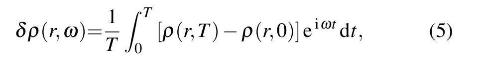
The nitrogen doping concentration affects the energy gap and lattice constant.When the N-doped graphene nanostructure is used as an electrode material for supercapacitors,the nitrogen doping concentration also affects the specific heat capacity and the stability.To probe into the influence of the doping concentration on plasmonic stimulation,we compute the absorption spectra of nN-doped systems(Fig.4).Systems with different nitrogen doping concentrations are denoted as follows:1N(doping concentration 1.25%;one doping nitrogen atom,3#),2N(doping concentration 2.5%;two doping nitrogen atoms 3#and 7#),3N(doping concentration 3.75%;nitrogen atoms,3#,7#,and 8#),4N(doping concentration 5%;four doping nitrogen atoms,3#,7#,8#,and 9#),5N(doping concentration 6.25%;five doping nitrogen atoms 3#,7#,8#,9#,and 10#),and 6N(doping concentration 7.5%;six doping nitrogen atoms 3#,7#,8#,9#,10#,and 11#).The pulse stimulation polarized along the x axis weakens the intensities of the optical absorptions of the 2N,1N,6N,3N,4N,and 5N-doped systems and red-shifts the spectral lines of the 6N,4N,1N,2N,3N,and 5N-doped systems adjacent to energy resonance dot at 4.7 eV.The pulse stimulation polarized along the y axis weakens the intensities of the optical absorptions of 1N,3N,2N,6N,5N,and 4N-doped systems and red-shifts the spectral lines of the 2N,1N,5N,6N,3N,and 4N-doped systems adjacent to the energy resonance dot at 5 eV.It can be concluded that the increasing of doping amount is not correlated with a stronger optical absorption.In addition,the pulse stimulation polarized along the x axis results in the splitting of the optical absorption into two absorptions in all nN-doped systems adjacent to energy resonance dot at 5 eV due to the contribution of the 3#nitrogen atoms.
Fig.4.Dipole response(optical absorption)of N-doped graphene systems with six different nitrogen-doping concentrations obtained by pulse stimulation polarized in((a),(c))x axis and((b),(d))y axis directions.The numbers adjacent to the bars represent the quantities of nitrogen doping atoms.
To examine the influence of different types of doping atoms on the plasmonic stimulations of the graphene nanostructure,absorption spectra of doped graphene nanostructures with different types of atoms are obtained by pulse stimulation polarized in the x-axis(Figs.5(a)and 5(c))and y-axis(Figs.5(b)and 5(d))directions.For a clear comparison,the dipole response of pristine graphene is also shown in Fig.5.The doping atoms include boron,nitrogen,aluminum,silicon,phosphorus,and sulfur atoms.As the radius of boron atom and nitrogen atom are almost the same as that of carbon atom,the geometry of the graphene nanostructure remains unchanged after these atoms have been incorporated into the graphene.However,the geometry of the graphene nanostructure changes after aluminum,silicon,phosphorus,and sulfur atoms have been doped into the graphene due to their atom radii are different from that of carbon atom.The atom diameters of silicon,phosphorus,and sulfur are 1.6˚A larger than the thickness of one layer of the graphene nanostructure,and the aluminum atom diameter is 2.0˚A larger than the thickness of one layer of the nanostructure after geometric optimization.Furthermore,the graphene nanostructure is slightly deformed.
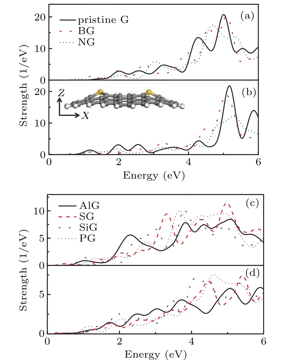
Fig.5.Dipole response(optical absorption)of doped graphene systems with two different types of atoms(doping concentration 2.5%)obtained by pulse stimulation polarized in((a),(c))x-axis and((b),(d))y-axis directions.The two doping atoms are at positions 3#and 7#.Inset in panel(b)represents the side view of geometrically optimized Si-doped graphene nanostructure.
Doping of graphene with different heteroatoms results in higher sensitivities to different molecules,and the relevant applications have been reported in Refs.[61–65].Aldoped graphene is more sensitive to the adsorption of CO than pure graphene and N-doped graphene,which was revealed by a theoretical study.[66]The adsorption of CO on the pristine graphene surface is considered as physisorption,while what occurs on aluminum-doped graphene is chemisorption.
The introduction of nitrogen(or P,B)atoms into sp2-hybridized carbon frameworks of graphene is generally effective in modifying the electrical properties and chemical activities,which has been demonstrated both theoretically and experimentally in Ref.[67].The N-doped graphene[68,69]is a promising candidate for replacing Pt-based catalysts in fuel cells due to its superior properties,such as excellent methanol tolerance in an alkaline medium,long-term stability,high catalytic activity,low cost,and environmental friendliness.The S-doped graphenesgraphene[70]also exhibits a similar superior electrocatalytic performance to that of the N-doped graphene.Shahrokh and Leonard reported that the optical conductivity of Si-doped graphene[71]is higher than that of pristine graphene in the visible range.These predicted optical and electronic properties can conduce to the designing of photovoltaic cells or similar systems.
As shown in Fig.5,a pulse stimulation polarized in the x-axis direction enhances the intensity of the optical absorption of the Si,Al,P,S,N,and B-doped systems adjacent to energy resonance dot at 5 eV.The pulse stimulation polarized in the y-axis direction enhances the intensity of the optical absorption of Al,Si,S,P,N,and B-doped system adjacent to energy resonance dot at 5 eV.Yet,the intensities of the optical absorption of all the doped systems are lower than that of the pristine system adjacent ext to energy resonance dot at 5 eV.
The reduced optical absorption of doped graphene is attributed to the doping atoms that break the symmetry of these configurations.The pulse stimulation polarized in the x-axis direction blue-shifts the dipole response line of the B-doped system and red-shifts that of the N-doped system in comparison with those of the pristine system adjacent to energy resonance dots at 5 eV.However,the pulse stimulation polarized in the y-axis direction red-shifts the dipole response line of the B-doped system and blue-shifts that of the N-doped system in comparison with the pristine system adjacent to energy resonance dot at 5 eV.In both cases,their scenarios are opposite truly.Doped atom with a size similar to carbon atom,such as boron atom and nitrogen atom,results in a lower spectral attenuation.Systems with other doping atoms exhibit a significantly weaker optical absorption.Therefore,nitrogen and boron are promising candidates for the chemical doping of graphene nanostructures.
We also investigate the resonance frequency distribution of the induced charge response.Figure 6 shows the induced charge density distributions of doped graphene nanostructures with different types of atoms.The spatial distribution of the induced charge density of the Al-doped system is different from that of the B-doped system,as the distance between hole and electron is larger due to the metallic properties of aluminum.To the best of our knowledge,the plasmonic stimulation capability of metals is stronger than that of nonmetals.
In order to understand the contributions of different orbitals to the electronic state of doped graphene,the total density of states(TDOS)and partial density of states(PDOS)are calculated for XG(X=B,N,Al,S,Si,P).Figure 7 displays the total densities of states(TDOSs)and partial densities of states(PDOSs)calculated for monolayer XG.As seen in Fig.7,the PDOSs of XG reveal the contributions from both the s,p,and orbitals d of X(X=B,N,Al,S,Si,P)near the Fermi level.Obviously,the effects of the p orbitals of X(X=B,N,Al,S,Si,P)on the TDOS are much more pronounced than those of the s and d orbitals except SG.For SG,the effects of the d orbitals of X(X=B,N,Al,S,Si,P)on the TDOS are much more pronounced than those of the s and p orbitals.

Fig.7.Total density of states(TDOS)and partial density of states(PDOS)of XG(X=(a)B,(b)N,(c)Al,(d)S,(e)Si,and(f)P).
4.Conclusions
The collective stimulations of doped graphene systems are studied in detail by TDDFT.The obtained conclusions are summarized below.
(i)The optical absorption intensities of all the doped graphene systems adjacent to energy resonance dot at 5 eV are stronger for pulse stimulations polarized in armchair-edge orientation than for pulse stimulations polarized in zigzag-edge orientation.
(ii)For different positions of nitrogen dopants,it is found that a higher degree of symmetry destruction is correlated with weaker optical absorption.Therefore,it is very important to choose the optimal doping location.
(iii)For the concentration of nitrogen dopants,the number of dopants is not correlated with a stronger optical absorption.An appropriate doping concentration can effectively avoid excessively attenuating the optical absorption.
(iv)For different doping atoms,the optical absorption of doping atom of a size similar to carbon atom,such as boron atom and nitrogen atom,is less attenuated.Systems with other doping atoms exhibit a significantly weaker optical absorption.Nitrogen and boron are candidates for the chemical doping of graphene nanostructures.The effects of the p orbitals of X(X=B,N,Al,S,Si,P)on the TDOS are much more pronounced than those of the s and d orbitals except SG.
(v)The absorption spectra of all doped graphene nanostructures are split into the visible and ultraviolet range.Doped graphene presents a promising material for nanoscaled plasmonic devices with more effective absorption in the visible and ultraviolet range.
猜你喜欢
杂志排行

Chinese Physics B的其它文章
- Multiple solutions and hysteresis in the flows driven by surface with antisymmetric velocity profile∗
- Magnetization relaxation of uniaxial anisotropic ferromagnetic particles with linear reaction dynamics driven by DC/AC magnetic field∗
- Influences of spin–orbit interaction on quantum speed limit and entanglement of spin qubits in coupled quantum dots
- Quantum multicast schemes of different quantum states via non-maximally entangled channels with multiparty involvement∗
- Magnetic and electronic properties of two-dimensional metal-organic frameworks TM3(C2NH)12*
- Preparation of a two-state mixture of ultracold fermionic atoms with balanced population subject to the unstable magnetic field∗