Strain-dependent resistance and giant gauge factor in monolayer WSe2∗
2021-09-28MaoSenQin秦茂森XingGuoYe叶兴国PengFeiZhu朱鹏飞WenZhengXu徐文正JingLiang梁晶KaihuiLiu刘开辉andZhiMinLiao廖志敏
Mao-Sen Qin(秦茂森),Xing-Guo Ye(叶兴国),Peng-Fei Zhu(朱鹏飞),Wen-Zheng Xu(徐文正),Jing Liang(梁晶),Kaihui Liu(刘开辉),and Zhi-Min Liao(廖志敏)
State Key Laboratory for Mesoscopic Physics and Frontiers Science Center for Nano-optoelectronics,School of Physics,Peking University,Beijing 100871,China
Keywords:strain engineering,van der Waals materials,symmetry breaking,orbital magnetization,Berry curvature
1.Introduction
Two-dimensional(2D)van der Waals(vdW)layered transition metal dichalcogenides(TMDCs),such as MoS2and WSe2,have demonstrated potential applications in the nextgeneration electronics owing to their remarkable electrical,optical,and mechanical properties.[1–5]Unlike the bulk semiconducting materials that are usually brittle,it is reported that TMDCs can exceptionally sustain in-plane strain as high as 11% in their monolayer counterparts,[6]promising for the high-performance flexible and transparent electronics.[7–10]Based on their high flexibility,extensive theoretical and experimental studies have recently been motivated by the interests for strain engineering.[11–28]It is found that strain can significantly affect the physical properties of TMDCs.Giant valley shift[21]and bandgap engineering[11,12,14,16]can be achieved by introducing uniaxial strain in monolayer TMDCs.Importantly,strain is also proposed to manipulate the Berry curvature,[21,28]which is generally important in the topological transport.The uniaxial strain can break the C3vsymmetry and thus induce an asymmetrically distributed Berry curvature in a single valley,i.e.,nonzero Berry curvature dipole in monolayer TMDCs,leading to the nonlinear Hall effect.[28]Furthermore,the strain is known to induce pseudo-magnetic field in 2D materials,which has been predicted and experimentally found to generate zero-field quantum Hall effect by forming Landau levels.[17,25,26]Additionally,for the TMDCs with orthorhombic phase,such as the Weyl semimetal MoTe2,it is reported that the strain can effectively tune the Weyl points,resulting in the phase transition from type-II to type-I Weyl semimetals.[29]Interestingly,in the twisted TMDCs proposed recently,the formation of moir´e pattern can be actually regarded as strain engineering as well,which can result in various exotic phenomena including spin-liquid states,emergent magnetic order,and chiral superconductors.[30]Due to their high flexibility and strain-tunability,TMDCs provide an ideal platform to study the strain engineering of transport properties.
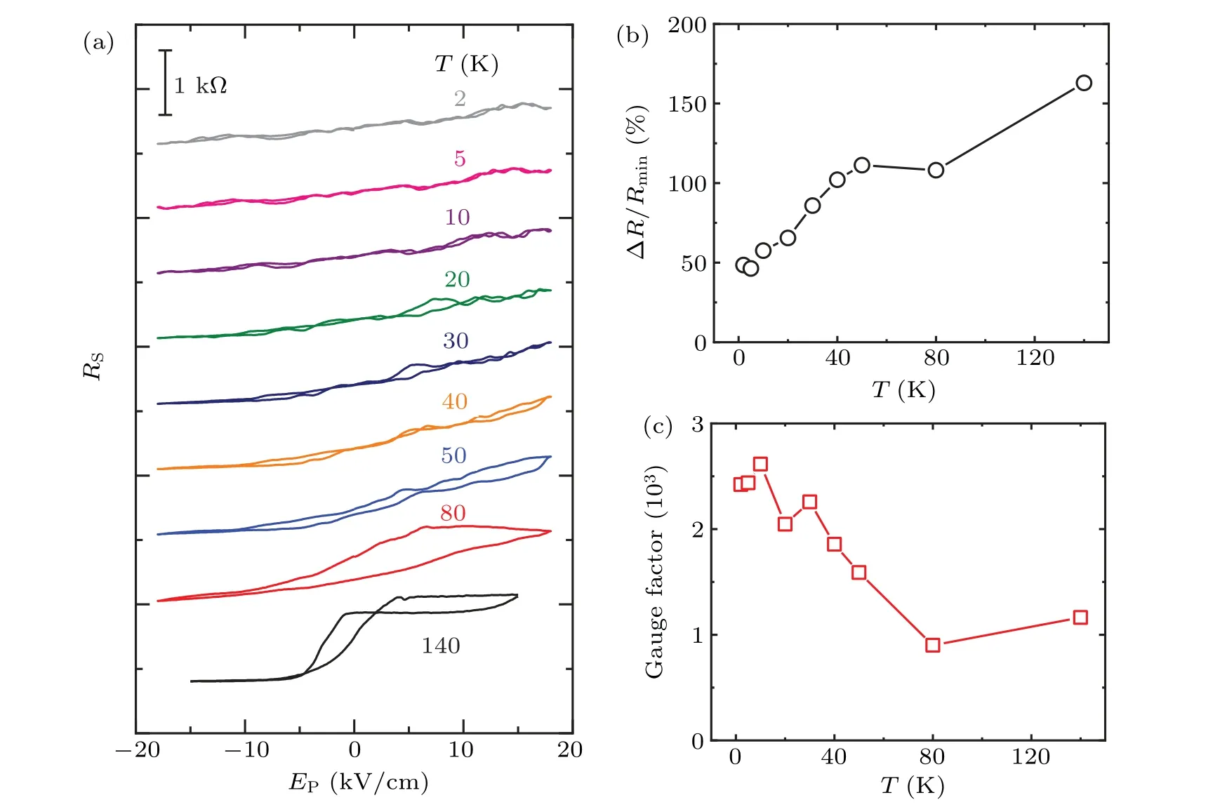
In this work,we investigate the strain-dependent resistance of the ionic gated monolayer WSe2,where giant gauge factor at various temperature ranges is obtained.We produce uniaxial strain by the inverse piezoelectric effect of(1−x)Pb(Mg1/3Nb2/3)O3]–x[PbTiO3](PMN-PT)with very high piezoelectric coefficient.[31–35]Under uniaxial tensile strain,the sheet resistance of WSe2dramatically changes.The extracted gauge factor is approximately 1100 at 140 K and is further enhanced to~2400 at 2 K.This giant gauge factor is attributed to the strain-modulated mobility,which is reduced by the magnetic scattering induced by net orbital magnetization associated with nonzero Berry curvature dipole.Our work paves the way to enhance the strain sensitivity by manipulating the Berry curvature in 2D materials.
2.Experiment and method
WSe2flakes were exfoliated from bulk crystals onto silicon wafer with 285 nm SiO2.Monolayer WSe2was identified by optical contrast and fluorescent microscopy.Then the monolayer WSe2was transferred onto the PMN-PT substrate by using a pick-up transfer technique.[36]Detailed topography of the transferred WSe2was imaged by the atomic force microscopy to resolve the possible ruptures and bubbles.Subsequently a uniform part of WSe2was selected to pattern into a standard Hall-bar geometry.Electrical contacts were made by e-beam lithography followed by e-beam evaporation of Ti(1 nm)/Au(50 nm)and lift-off in acetone.It is worth noting that the electrodes applying electric field to the PMN-PT substrate were designed along the[001]orientation of the PMNPT,by which the uniaxial strain can be produced.The strain in the monolayer WSe2introduced by the PMN-PT substrate was confirmed by the second-harmonic generation(SHG)spectroscopy.WSe2was heavily hole doped into metallic state by the ionic liquid technique and the low-temperature Ohmic contact was guaranteed.
3.Results and discussion

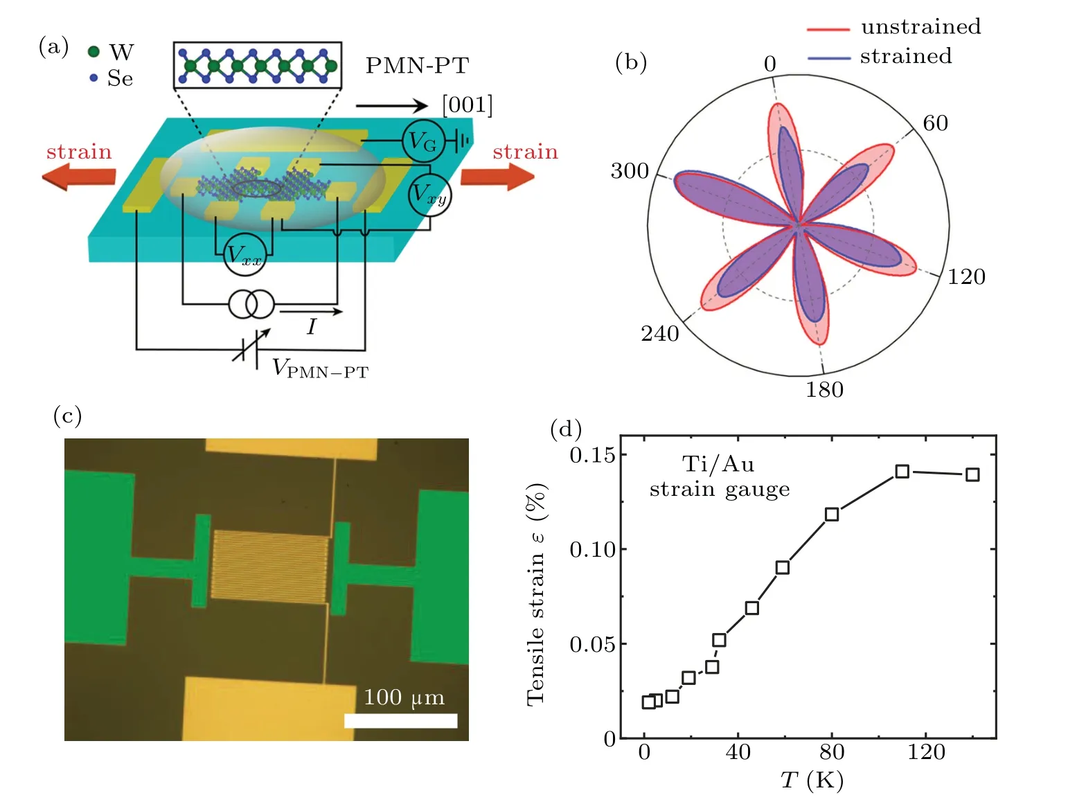
Fig.1.(a)Schematics of ionic gated monolayer WSe2 device.The polarization voltage was applied along the[001]orientation of the PMN-PT substrate to ensure the uniaxial tensile strain.(b)Polarization resolved second harmonic generation intensity pattern.Red line:unstrained monolayer WSe2.Blue line:strained monolayer WSe2.(c)The optical microscope image of the Ti/Au strain gauge.(d)Temperature dependence of the maximum tensile strain produced in the PMN-PT substrate with a fixed polarized electric field EP=18 kV/cm,measured by the Ti/Au strain gauge.
The device structure and measurement scheme are depicted in Fig.1(a).The ionic gate voltageVGwas fixed at−5 V and thus the holes in the valence bands at K/K′valleys dominated the transport properties.[37]Besides the gate volatge VG,an extra voltage was applied on the PMN-PT substrate after the ionic liquid was freezed below 180 K.An electric field EPwas produced between the electrodes along the[001]direction of the PMN-PT with the distance of 50µm.The uniaxial strain was induced along EPdirection into monolayer WSe2by the inverse piezoeletric effect of PMN-PT.To verify the strain in the WSe2,the SHG spectroscopy was measured.Polarization resolved SHG reflects the lattice symmetry of the probed crystals and the SHG intensity is susceptible to the mechanical deformation of the crystal lattice.[38,39]As shown in Fig.1(b),the SHG of the monolayer WSe2on the poled PMN-PT substrate is distorted from that of unstrained WSe2with the perfect D3hsymmetry,establishing the induced strain in WSe2by PMN-PT.For the quantitative description of the strain level,we patterned and deposited a strain gauge made up of Ti/Au(1 nm/50 nm in thickness)on the same PMN-PT substrate[Fig.1(c)]besides the deposition of the contact metal.The strain measured from the strain gauge can roughly reflect the controllable strain level that we apply to the WSe2.Figure 1(d)shows the temperature dependence of the maximum tensile strainεon the strain gauge induced by the PMN-PT substrate at EP=18 kV/cm,which decreases from 0.14% to 0.02% upon decreasing temperature from 140 K to 2 K.The decrease of the strain with decreasing temperature is consistent with the fact that the piezoelectric coefficient of PMN-PT decreases by a factor of 0.2 between 140 K and 5 K.[40]

Fig.2.(a)Sheet resistance of monolayer WSe2 as a function of EP measured at temperatures from 140 K to 2 K.The curves are shifted for clarity.(b)Ratio of percentual changes of the sheet resistanceΔR/Rmin×100%under the tensile strain and(c)gauge factor as a function of temperature.
Figure 2(a)shows the sheet resistance of monolayer WSe2as a function of EPmeasured at different temperatures.Before sweeping EP,we first polarized the PMN-PT along the[001]direction by applying EP=18 kV/cm for 15 min at 140 K to achieve a well aligned state and hence the initial strain in WSe2was fixed to be moderately tensile.Then we sweeped EPwith multiple cycling between EP=±18 kV/cm until the strain-induced sheet resistance change stabilized into an unipolar hysteretic loop,as shown in Fig.2(a).The emergence of the hysteretic behavior is due to the ferroelectricity nature of PMN-PT.[41]It is worth noting that the coercive field of PMN-PT is strongly temperature dependent and it increases exponentially as the temperature decreases.[42]The coercive field at low temperatures is(~35 kV/cm at 40 K[42])beyond the range of electric field that is achievable(±18 kV/cm)in this work.So as backward sweeping EPto−18 kV/cm,the piezoelectric polarization cannot be switched to the opposite direction at low temperatures.In other words,the tensile strain varies monotonously without sign change by sweeping EPfrom positive to negative value.From 140 K to 2 K,the hysteresis grows weak and finally disappears,as shown in Fig.2(a),which is also attributed to the increased coercive field upon decreasing temperature.


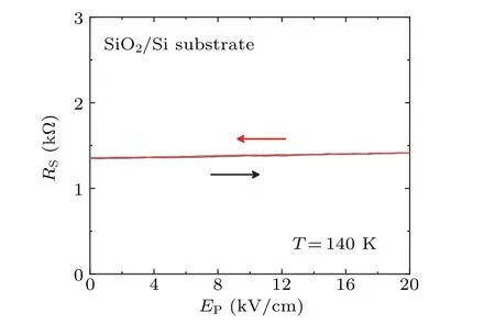
Fig.3.Sheet resistance of monolayer WSe2 as a function of EP measured at 140 K.The substrate is replaced by the non-piezoelectric SiO2/Si substrate.
It is worth noting that in addition to the strain effect,extrinsic mechanisms,such as side gate effect and the influence of EPon the ionic liquid,may also contribute to the changes of the sheet resistance of WSe2.However,these extrinsic mechanisms can both be ruled out in this work.Although the side gate can effectively tune the carrier density near the sample edges in a range of a few tens of nanometers in materials like graphene and InSb nanowire,[43–45]the carrier density in the ionic gated WSe2(~1013cm−2)is at least two orders of magnitude higher than that in those materials and hence the screening effect is prominent,which makes the side gating effect negligible in principle.We have performed a contrast experiment by using SiO2/Si substrate to eliminate the influence of EPon the ionic liquid.As sweeping EP,the negligible resistance change(less than 4%)and no hysteresis were observed at 140 K,as shown in Fig.3.
We have noticed that the strain-induced resistance change of TMDCs is previously ascribed to the bandgap engineering.[20]The gauge factor of monolayer MoS2has been reported by Kis et al.to be a relatively low negative value~−148 at 300 K.[20]However,the monolayer MoS2is undoped and semicoducting in that work.So the resistance change is attributed to the reduced bandgap induced by tensile strain.[14]We stress monolayer WSe2used here is in the metallic phase with heavily hole-doping.Since the Fermi level is far from the band edge,the bandgap engineering can be safely excluded as the main cause of the giant gauge factor here.

Here we attribute the strain engineering of mobility to the strong magnetic scattering associated with nonzero Berry curvature dipole.For monolayer TMDCs,large Berry curvature emerges at K/K′valleys due to the spontaneous inversion symmetry breaking.[28]Berry curvature plays an important role in the topological transport,which would induce the transverse deflection of electron movement.[46]The presence of time-reversal symmetry in TMDCs leads to the opposite signs of Berry curvature in opposite valleys.Thus,driven by an in-plane electric field E,the electrons at opposite valleys will deflect along opposite directions and cancel with each other,leading to a charge neutral valley current,known as valley Hall effect.[46]In addition to Berry curvature,the dipole moment of Berry curvature,i.e.,Berry curvature dipole,would also induce anomalous transport phenomena.However,the Berry curvature has a symmetric distribution in a single valley constrained by the C3vsymmetry,leading to vanishing Berry curvature dipole,which exactly describes the asymmetric distributions of Berry curvature.[47]Applying uniaxial strain can break the C3vsymmetry in monolayer TMDCs,inducing nonzero Berry curvature dipole.The Berry curvature dipole D is proposed to generate a net out-of-plane orbital magnetization M∝D·E when an external electric field E is also applied.[47]The emergent orbital magnetization can induce a Hall current as a second-order response to E,that is,the nonlinear Hall effect.[46]As shown in Fig.4(c),the nonlinear Hall effect has been observed in a typical strained monolayer WSe2.The emergent second-harmonic Hall voltage can be well fitted by a parabolic curve[the red line presented in Fig.4(c)],suggesting the existence of nonlinear Hall effect.[28]Moreover,such orbital magnetization can also introduce additional magnetic scattering,thus reducing the mobility and longitudinal conductance.Obviously,a larger Berry curvature dipole means larger orbital magnetization,inducing the stronger suppression of mobility.Note previous studies on the nonlinear Hall effect in strained WSe2have shown that Berry curvature dipole could be significantly enhanced by increasing the tensile strain.[28,47]Thus,here the measured giant gauge factor can be ascribed to the strain induced additional magnetic scattering associated with a nonzero Berry curvature dipole.Furthermore,as shown in Fig.4(d),the temperature dependent resistance of WSe2shows a metallic behavior at high temperature,while it increases upon decreasing temperature below 40 K.Such temperature-dependent behavior is also consistent with the existence of magnetic moments,which can lead to the Kondo effect and a minimum resistance.
4.Conclusions
We have demonstrated a strong dependence of resistance on uniaxial strain in monolayer WSe2at various temperatures.The gauge factor can reach as large as 2400,demonstrating great application potential for the next-generation ultrasensitive sensors.We attribute this strain-dependent resistance to the strong magnetic scattering associated with nonzero Berry curvature dipole induced by strain.Our work indicates that the performance of strain sensors can be effectively improved by modulating the Berry curvature via changing the symmetry in 2D vdW materials,which should be promising for highly sensitive strain sensors and flexible electronics.
猜你喜欢
杂志排行
Chinese Physics B的其它文章
- Origin of anomalous enhancement of the absorption coefficient in a PN junction∗
- Protection of isolated and active regions in AlGaN/GaN HEMTs using selective laser annealing∗
- First-principles study of plasmons in doped graphene nanostructures∗
- Probing thermal properties of vanadium dioxide thin films by time-domain thermoreflectance without metal film∗
- An improved model of damage depth of shock-melted metal in microspall under triangular wave loading∗
- Signal-to-noise ratio of Raman signal measured by multichannel detectors∗
