Ohmic and Schottky contacts of hydrogenated and oxygenated boron-doped single-crystal diamond with hill-like polycrystalline grains∗
2021-09-28JingChengWang王旌丞HaoChen陈浩LinFengWan万琳丰CaoYuanMu牟草源YaoFengLiu刘尧峰ShaoHengCheng成绍恒QiLiangWang王启亮LiuAnLi李柳暗andHongDongLi李红东
Jing-Cheng Wang(王旌丞),Hao Chen(陈浩),Lin-Feng Wan(万琳丰),Cao-Yuan Mu(牟草源),Yao-Feng Liu(刘尧峰),Shao-Heng Cheng(成绍恒),2,†,Qi-Liang Wang(王启亮),2,‡,Liu-An Li(李柳暗),and Hong-Dong Li(李红东),2,§
1State Key Lab of Superhard Materials,College of Physics,Jilin University,Changchun 130012,China
2Shenzhen Research Institute,Jilin University,Shenzhen 518057,China
Keywords:CVD diamond film,boron-doped diamond film,ohmic contact,Schottky junction
1.Introduction
As an extremely functional material with excellent properties,for example a wide bandgap,high thermal conductivity,high electron and hole mobility,high breakdown voltage,chemical inertness and biocompatibility,[1,2]diamond has been widely applied in high-frequency and high-power electronic devices,including Schottky barrier diodes,PN diodes and field-effect transistors.[3]Device performances,especially the breakdown field,are still far below the theoretical limit of diamond.A thicker epitaxial layer with good crystalline quality and low defect density is required to suppress the leakage current and realize high breakdown voltage.[4]
Although single-crystal diamond(SCD)films with a thickness of up to a few millimeters and a diameter of 2 inch have been achieved,the control of point and extended defects in the crystals remains challenging.[5]Various kinds of defects,such as dislocations with number density higher than 104cm−2[6]and/or hill-like polycrystalline grains(HDPGs),are found on the surface of diamond films epitaxy grown by chemical vapor deposition(CVD).[7]The defects generally originate from the substrate dislocations and surface defects introduced by mechanical polishing.The defects near the surface present as the recombination centers of electrons and holes,which greatly reduce the carrier mobility of diamond and restrict application in electronic devices.[8]As p-type conduction by boron doping is normally necessary for application in electronic devices,the introduction of boron will further degrade the crystalline quality and increase the defect density(dislocations,twin crystals,holes,etc.).[9,10]Previous works generally focused on the growth conditions(gas ratio,pressure,temperature,etc.)required to decrease the number of defects and improve the quality of wafer.[11,12]However,the influence of defects(especially for some polycrystalline grains in SCD)on the electrical properties of semiconductor diamond devices has not been investigated extensively,and knowledge about this may be useful for constructing junctions or improving electrode contact.
Herein,by adjusting the CVD growth process of the heavily boron-doped p+SCD film,the high-density polycrystalline grains appear to extend to the SCD surface,where a relatively higher boron concentration is present.The leakage path and ohmic contact to the gold(Au)electrode are demonstrated and the electrical conductivity is related to the type of surface termination(oxygenation or hydrogenation).Interestingly,different rectification characteristics are found in oxygen-terminated HPDG and SCD,determined by differences in boron doping levels.
2.Experimental details
Heavy boron-doped p+SCD films were homoepitaxially grown on high-temperature–high-pressure(HTHP)synthesized insulating(100)SCD with a size of 3 mm×3 mm×1 mm by microwave plasma CVD(MPCVD)at 2.45 GHz.The substrate was chemically cleaned with a mixed acid solution of H2SO4:HNO3(1:1)at 250°C for 1 h in order to remove surface impurities,followed by ultrasonic cleaning with acetone and alcohol for 10 min,respectively.Gaseous hydrogen(H2)and methane(CH4)with a CH4/H2ratio of 3% were used as the reaction sources,and the boron dopant was introduced by trimethylboron(B(CH3)3)at a B/C of 8000 ppm.At a pressure of 9.5 kPa,the substrate temperature was approximately 830°C during the 50 h growth process.The surface morphology and doping behavior were characterized by scanning electron microscope(SEM)and Raman spectroscopy.Current–voltage(I–V)curves were measured with gold probes by a Keithley 2450 source meter.
3.Results and discussion

Fig.1.SEM images of boron-doped p+single-crystal diamond(SCD)with hill-like polycrystalline diamond grains(HPDGs).The top inset is an enlarged image of grains at high magnification.The bottom inset is a crosssectional image of polycrystalline grains in the film.
A SEM image of the as-grown boron-doped diamond(BDD)film is shown in Fig.1.Compared with twodimensional step-flow homoepitaxial CVD SCD with a planar surface,HPDGs randomly appear on the smooth surface with a high density of 104cm−2,which is similar to the typical dislocation density of boron-doped diamond is in the order of 104cm−2.The enlarged picture of the polycrystalline grains(top inset)show a lamellar-twining feature,similar to typical heteroepitaxial polycrystalline BDD films.[6]The crosssectional image of the sample(bottom inset)shows that these polycrystalline grains begin about 100µm beneath the top surface and continuously extend along the(100)orientation showing V-shaped columnar growth.During initial growth of the HPDGs,the grains are relatively small with abundant grain boundaries,[13]following V-shaped columnar growth with enhanced grain size and less grain boundaries.The appearance of the polycrystalline grains is generally related to the original intrinsic structural defects(e.g.,dislocations,growth steps,scratches during polishing,etc.)of the HTHP substrate and/or some external dust deposited on the polished surface.[7]Two-dimensional epitaxial growth would be disturbed due to lattice mismatch around the defect region,leading to threedimensional growth and a second nucleation.The structural morphology of the defects is similar to reports in previous literature.[6,7,11,12]

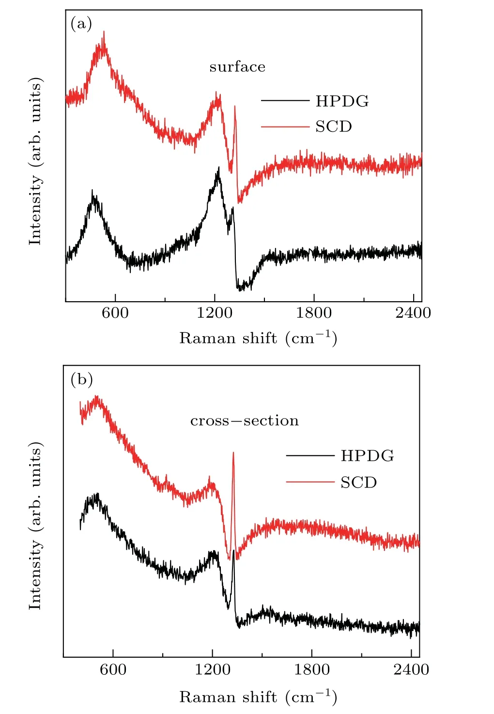
Fig.2.Raman spectra recorded from the HPDG and SCD regions on the surface(a)and cross-section(b)of boron-doped diamond films.
The Raman spectral characteristics were performed for the surface and cross section,as presented in Fig.2.On the top surface(Fig.2(a)),comprising the HPDG and the SCD regions,the red shift and asymmetric peaks centered at around 1320 cm−1comparing to the zero phonon vibration mode(1332 cm−1)of intrinsic diamond are related to the Fano effect for heavy boron doping(>1019cm−3)two broad bands at around 480 cm−1and 1200 cm−1appear to be dependent on the two maxima of the phonon density of states of diamond.[14,15]It can be seen that the boron concentration near the HPDG region is higher than that of the SCD surface,depending on the surface according to Fano asymmetry and the relative intensity between the 1200 and 1320 cm−1bands.[16]The Raman spectra recorded from the cross section(Fig.2(b))present a similar trend,i.e.,boron concentration of HPDG is higher than that of the SCD region.The boron concentration[B]can be quantitatively estimated by fitting the 480 cm−1band according to the following imprecise empirical law:[17][B](cm−3)=8.44×1030×exp[−0.048W(cm−1)],where W is the wavenumber of the Lorentzian component of the 480 cm−1broad peak.The calculated boron concentration of the HPDG region on the surface(cross section)is approximately 1.1×1021cm−3(2.4×1021cm−3),two(four)times higher than that of SCD region,5.4×1020cm−3(6.5×1020cm−3).Previous work showed that the boron concentration at grain boundaries is higher than that in grains.[18]Therefore,HPDGs with more grain boundaries(especially on the growth surface)have a higher boron doping concentration than SCD on both surface and cross-sectional aspects.
The I–V characteristics on surfaces with HPDG and SCD contacts were measured using a Keithley 2450 source meter with two gold(Au)probes(inset of Fig.3).Obviously,the conductivity characteristic between two adjacent HPDGs of the as-grown sample(hydrogen-terminated surface)has a nearly linear I–V curve,as shown in Fig.3(a),implying the formation of an ohmic-like contact.[19]Although the current obviously decreases,a linear I–V curve is maintained for the neighboring oxygen-terminated HPDG surface after acid boiling treatment(Fig.3(b)),as surface oxygenation could increase the resistance of BDD.[20,21]For comparison,the I–V curve obtained from the hydrogen-terminated SCD surface in the as-grown sample is also nearly linear and has a similar current density(Fig.3(c))comparing to the case in Fig.3(a).However,oxygen termination changes the I–V curve,giving it symmetry rectification characteristics(Fig.3(d)),which could be ascribed to the formation of a back-to-back Schottky diode(as discussed in the following paragraph).Based on these results,we can conclude that the surface termination can modulate the contact properties,especially for SCD with a lower boron concentration relative to HPDG.

Fig.3.The I–V curves for the hydrogen-terminated HPDG(a)and SCD(c),and oxygen-terminated HPDG(b)and SCD(d).Insets in(a)and(c)are schematics of the measurement configuration.
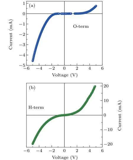
Generally,the surface of diamond after homoepitaxial growth is hydrogen terminated,because the main gas source in the MPCVD chamber is hydrogen.On the one hand,hydrogen termination provides a negative electron affinity of 1.3 eV and helps to upshift the energy band of diamond.[22,23]On the other hand,hydrogen termination generates a high concentration of two-dimensional hole gas(2DHG)on the surface,resulting in upward band bending and high surface conductance.[24]Those two factors can significantly reduce the Schottky barrier height between Au(with a work function of approximately 5.0 eV)and diamond,resulting in an ohmic-like contact(Figs.3(a)and 3(c)).For oxygen termination,the electron affinity of the diamond surface can be easily adjusted by the C–O bonds,which gives a positive electron affinity of approximately 0.5 eV.In addition,unlike‘transfer doping’in hydrogen-terminated diamond which forms a 2DHG channel,the oxygen-terminated surface is nearly insulate.Those two factors cause the Au/diamond contact to be a Schottky contact.[25]Therefore,the two Au/diamond contacts form a back-to-back Schottky diode,leading to a symmetry rectification characteristic(Fig.3(d)).On the other hand,the relatively higher boron doping concentration in the HPDG will broaden the acceptor energy band near the top of the valence band.[26]In addition,the high density of dangling bonds and distorted sp2-bonded carbon at the grain boundaries introduce broadπandπ∗defect states in the bandgap of diamond.[27]Those two factors act as a conducting channel,facilitating easy tunneling of the hole,which can weaken the termination dependence and facilitate the formation of an ohmic contact(Fig.3(b)).This assumption is confirmed by putting two probes on the oxygen-terminated HPDG and SCD regions,respectively,showing an obvious rectification characteristic,as expected(Fig.4(a)).Reversibly,the I–V curve returns to symmetry when the sample was re-treated(Fig.4(b)).

Fig.4.The I–V curve between SCD and HPDG with(a)an oxygenterminated and(b)a hydrogen-terminated surface.The inset in(a)is a schematic of the measurement configuration.
The modulation of contact properties by the type of surface termination can be explained from the variation of the conduction path related to the surface termination and bulk diamond material.As shown in Fig.5(a),the conduction path consists of three main parts:the Au/diamond contact(path①),surface conduction(path②)and bulk diamond conduction(path③).For the SCD region with hydrogen termination,the conduction is dominated by the ohmic contact as well as surface conduction,showing a relatively lower resistance than bulk diamond.However,oxygen termination changes path①into a Schottky contact and pinches off the surface conduction(Fig.5(c)),resulting in rectification characteristics with high resistance and a small current.Due to the existence of polycrystalline grains,the ohmic contact(a nearly linear I–V curve)between Au and HPDG(path①)is retained,even with oxygen termination.But the pinch-off of the surface conduction path increases the total resistance and decreases the current density(Fig.5(d)).At a hydrogen termination,the ohmic contact(nearly linear I–V curve)remains between the HPDGs,and the resistance decreases and the current density increases due to the opening of the surface conduction(Fig.5(b)).For both oxygen termination and hydrogen termination,the high boron concentration of HPDG determines that the conductivity tends to an ohmic contact.Based on the discussion above,HPDGs provide an approach to construct junctions or improve electrode contacts on doped semiconductor SCD.Controlled growth of HPDG can be realized by a selective area growth method.Firstly,a dielectric or metal layer is deposited on the diamond surface,which serves as mask.The mask in the HPDG area is then selectively removed by wet etching.After introducing artificial lattice damage via various etching process,we can control the following growth of HPDG.
4.Conclusion
In this study,HPDGs appear on heavy boron-doped p+single-crystal diamond film by prolonging the MPCVD grow duration.The polycrystalline grains originate from dislocation defects on the SCD surface and re-nucleation growth induced by the boron doping.The polycrystalline regions have a relatively higher boron concentration with respect to that on single crystal surfaces.
The I–V characteristics measured with two gold probes indicate that the I–V curve obtained from single-crystalline regions on an as-grown sample are nearly linear showing ohmic contact.A back-to-back Schottky diode could be formed after oxygen termination.This result confirms that the Au/diamond contact can be modulated by the type of surface termination.For the HPDG regions,the nearly linear I–V curve is retained for both oxygen termination and hydrogen termination,implying the ohmic contact is always maintained between Au and polycrystalline regions.This result experimentally confirms that the grains with abundant boundaries result in leakage paths and affect the contact properties.Therefore,HPDGs provide an approach to construct junctions or improve electrode contacts on doped semiconductor SCDs or devices.
猜你喜欢
杂志排行
Chinese Physics B的其它文章
- Multiple solutions and hysteresis in the flows driven by surface with antisymmetric velocity profile∗
- Magnetization relaxation of uniaxial anisotropic ferromagnetic particles with linear reaction dynamics driven by DC/AC magnetic field∗
- Influences of spin–orbit interaction on quantum speed limit and entanglement of spin qubits in coupled quantum dots
- Quantum multicast schemes of different quantum states via non-maximally entangled channels with multiparty involvement∗
- Magnetic and electronic properties of two-dimensional metal-organic frameworks TM3(C2NH)12*
- Preparation of a two-state mixture of ultracold fermionic atoms with balanced population subject to the unstable magnetic field∗
