Nanoscale structural investigation of Zn1−xMgxO alloy films on polar and nonpolar ZnO substrates with different Mg contents∗
2021-09-28XinLiang梁信HuaZhou周华HuiQiongWang王惠琼LihuaZhang张丽华KimKisslingerandJunyongKang康俊勇
Xin Liang(梁信),Hua Zhou(周华),Hui-Qiong Wang(王惠琼),3,‡,Lihua Zhang(张丽华),Kim Kisslinger,and Junyong Kang(康俊勇)
1Key Laboratory of Semiconductors and Applications of Fujian Province,Collaborative Innovation Center for Optoelectronic Semiconductors and Efficient Devices,Department of Physics,Xiamen University,Xiamen 361005,China
2School of Physics,Shandong University,Jinan 250100,China
3Department of Physics,Xiamen University Malaysia,Sepang 43900,Selangor,Malaysia
4Center for Functional Nanomaterials,Brookhaven National Laboratory,Upton,New York 11973,USA
Keywords:Zn1−xMgxO films,molecular beam epitaxy,phase separation,transmission electron microscopy
1.Introduction
The development of technology requires the ability to monitor the optical band gap range of many optoelectronic materials from violet light waves to ultraviolet light waves.Band-gap engineering is an effective strategy to solve this problem.A common method is to alloy ZnO with MgO.ZnO is a II–VI direct band gap semiconductor with a band gap of 3.37 eV and a large exciton binding energy of 60 meV at room temperature,and can be crystallized into a hexagonal wurtzite structure(a=3.25˚A,c=5.20˚A).[1,2]MgO is a typical cubic structure with an optical band gap of approximately 7.8 eV.[3]This alloy material(Zn1−xMgxO)can achieve tunable bandgaps from 3.37 eV to 7.8 eV.[4]Therefore,Zn1−xMgxO alloy films have broad potential applications in deep ultraviolet light-emitting diodes,solar-blind photodetectors,etc.[5,6]Nonetheless,these optoelectronic devices require a band gap larger than 4.0 eV for a Zn1−xMgxO film with an Mg content of more than 45%.This requirement often results in the formation of mixed-phase structures in the Zn1−xMgxO films.[7,8]However,the mixed phase is unstable due to the large difference in the phase structures between ZnO and MgO,especially when the Mg content is between 37% and 62%.[9,10]The unstable mixing phase in alloy films is usually accompanied by numerous grain boundaries.[11,12]Understanding these complex boundary structures is a key step to improve the stability of the mixing phase and the optoelectronic performance of this semiconductor,especially at a high Mg content of more than 62%.
On the other hand,integrating semiconductor ZnO with cubic materials that have unique properties has recently been increasingly studied.[13,14]For example,novel optoelectronics and memory devices have been fabricated by combining SrTiO3,[15]which exhibits an abundance of physical properties,such as two-dimensional(2D)electron gas,[16]ferroelectricity,[17]magnetism,[18]and superconductivity.[19]Similarly,integrating perovskite Pb(Zr,Ti)O3,[20]SrRuO3,[21]and BiFeO3[22]with wurtzite ZnO promotes faster response time and the production of more efficient field-effect transistors or resistance random access memory devices.In thermal equilibrium,ZnO is hexagonal wurtzite,while the crystal structure of MgO is cubic rock salt.For higher Mg(x>0.5)concentrations,cubic Zn1−xMgxO with a band gap energy higher than 5 eV has been obtained,as well as a direct energy band structure.[23–25]Therefore,this material has high potential application values due to the perspective of developing optical functions in the deep ultraviolet region.
MgO has a representative simple cubic structure and is widely used as a buffer layer on a wurtzite structure substrate.[14,26,27]Therefore,the homoepitaxy of the cubic ZnxMg1−xO film on the wurtzite ZnO substrate provides a template for studying the boundary structure and interfacial structure between the cubic film and wurtzite substrate.To address these issues,we propose a Zn1−xMgxO alloy film epitaxy on ZnO substrates with different orientations and investigate the films and interfacial structures.In this work,Zn1−xMgxO alloy films were grown on polar c-plane(0001)ZnO and nonpolar m-plane(10¯10)substrates by plasma-assisted molecular beam epitaxy(MBE).The Mg contents were examined by energy dispersive spectroscopy(EDS).The film and interfacial structures were revealed through x-ray diffraction(XRD)and transmission electron microscopy(TEM).
2.Zn1−xMgxO films preparation
MBE has the advantages of ultra-high vacuum growth environment,low film growth temperature,controllable growth process,and so on.The process of film growth by MBE involves the adsorption,decomposition,nucleation,and desorption of atoms or molecules,which is a kinetic process.So it can be used to prepare epitaxial film layers that cannot be prepared by traditional thermal equilibrium growth methods.Therefore,we used MBE to deposit Zn1−xMgxO thin films.A series of Zn1−xMgxO films were grown by MBE on(0001)-and(10¯10)-ZnO substrates.Before growth,all substrates were treated in the growth chamber by annealing at 350°C for 60 min in an oxygen plasma with an O partial pressure of 1×10⁻³Pa and a power of 250 W.The Zn1−xMgxO films were then deposited for 2 h,with the oxygen partial pressure maintained at 1×10⁻³Pa and the power of the oxygen plasma changed to 200 W,while the substrate temperature was increased to 400°C.At the same time,magnesium and zinc beams were injected toward the substrate with the adjustment of the temperature of the beam source furnace to tune the Mg/Zn ratio.The as-grown films were then annealed for 30 min with the substrate temperature maintained at 400°C(O partial pressure~1×10⁻³Pa,O plasma power~200 W)to reduce defects.
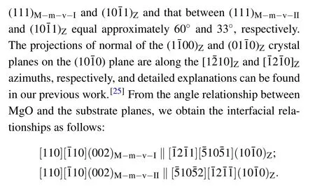
3.XRD results and discussion
To obtain the Mg content(x)and Zn content(1−x)in the Zn1−xMgxO films with different alloy compositions,which was achieved through the control of the Mg:Zn flux ratios,we characterized the Mg and Zn concentrations by EDS(Thermo Fisher,Czech Republic).Here,we defined the concentration of Mg plus Zn to be 100%.Figure 1 shows the Mg contents of the Zn1−xMgxO films grown on the c-plane(0001)ZnO and the m-plane(10¯10)ZnO.The Mg content x nearly linearly increases from approximately 19% to 75% with an increasing temperature of the magnesium beam source furnace(Mg source temperature)from 340°C to 400°C,and the Zn content decreases from approximately 81% to 25%.In addition,the proportions of Mg in the two sets of films are roughly the same at equal evaporation source temperatures of magnesium.
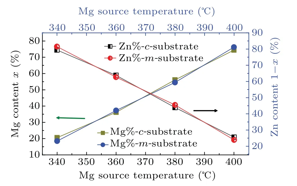
Fig.1.Mg content of the Zn1−xMgxO films from EDS.
Figures 2(a)and 2(b)show the XRD(Rigaku,Japan)results from the Zn1−xMgxO alloy films grown on the c-ZnO substrate with different Mg contents using a Cu Kαradiation source(1.54056˚A).The black curved lines are from the substrates as a comparison to the films.Apparently,the alloy films grown on the c-plane(0001)ZnO substrate show a peak of cubic phase MgO with an Mg content between 20.6%and 56.1%,as shown by the black arrow in Fig.2(a);this result is indicative of the appearance of phase separation.Figure 2(b)presents an amplified image of the rectangular area in Fig.2(a),which shows that as the Mg content increases,there is a slight increase in the MgO(002)peak and a shift in the peak position from 42.4°to 42.6°,as marked by the black circles and dashed line.This result indicates an increase in the proportion of the cubic phase with a decrease in the lattice length from 4.24˚A to 4.26˚A as the Mg content increases.Moreover,the XRD result reveals a(111)orientation of the cubic phase at 36.8°when the Mg content reaches 74.4%,as labeled by the blue arrow in Fig.2(b).This phenomenon reflects that the Mg content of 74.4%is able to trigger multiple growth orientations of the cubic phase for the alloy film on the c-substrate.Furthermore,the(002)peak of the cubic phase splits into two peaks.One is at 42.1°and the other at 42.8°,as marked by the red arrows in Fig.2(b),corresponding to the Zn1−xMgxO phase with a cubic structure and bulk-like cubic MgO,respectively.Therefore,at an Mg content of 74.4%,the alloy film exhibits an interesting feature of 2nd-order phase separation.Regarding the Zn1−xMgxO alloy films grown on the m-substrate,it is remarkable that no phase separation is observed for the Mg content at 18.5%(shown with a red curve in Fig.2(c)).When the Mg content reaches 37.3%(shown with a blue curve in Fig.2(c)),an obvious(002)peak and weaker(022)peak of the cubic phase start to appear in Fig.2(c).Similar to the case of the alloy films grown on the c-ZnO substrate,the intensities of the(002)and(022)peaks related to the cubic phase increase with an increasing Mg content,accompanied by slight shifts in the peak positions,as labeled by the black circles and dashed lines in Fig.2(d);this result is shown by the amplified image of the area marked by the black rectangle in Fig.2(c).It is obvious that the Mg content promotes the phase separation as well as a new orientation of the cubic phase in the alloy film.
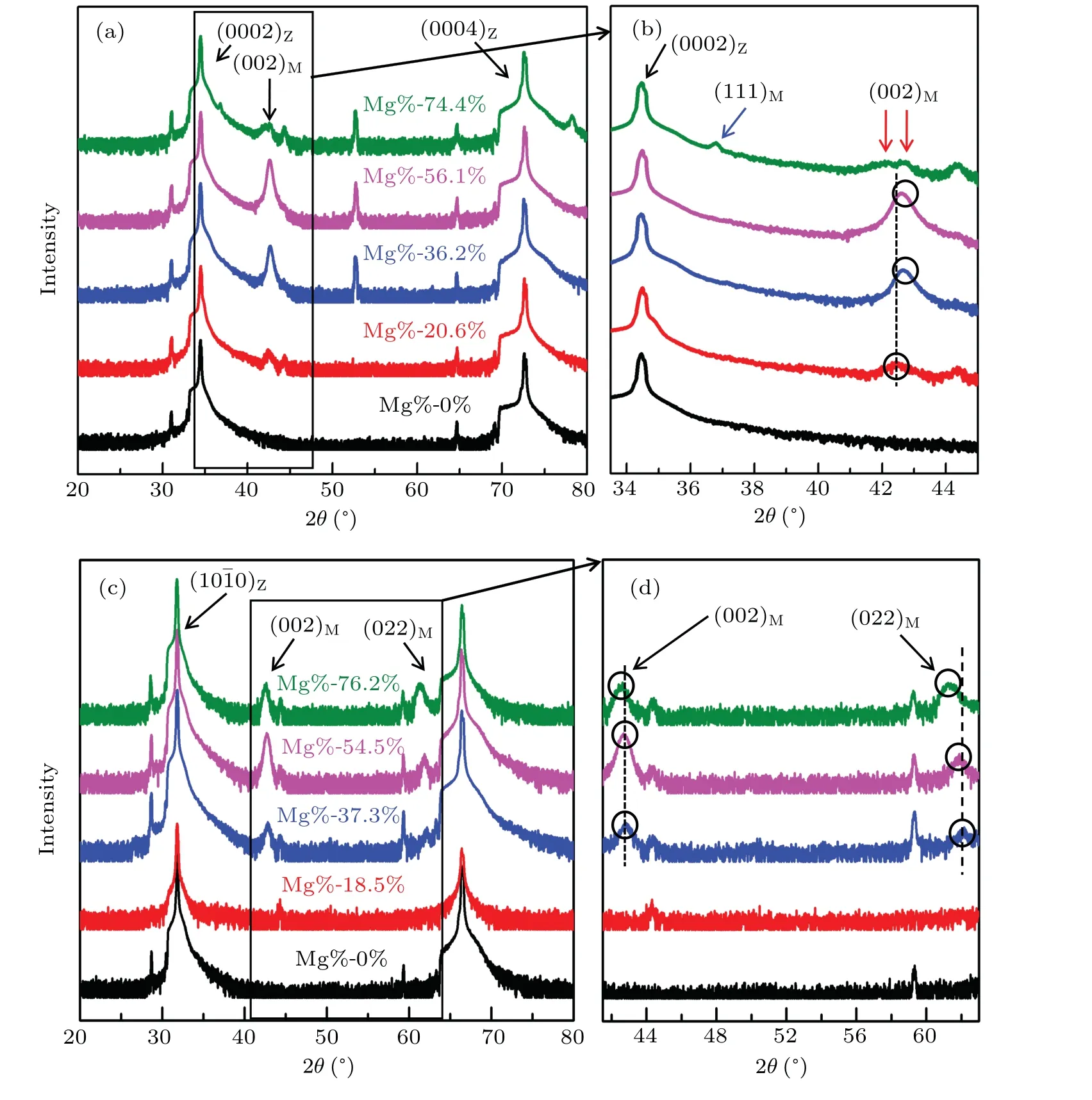
Fig.2.XRD results from the Zn1−xMgxO alloy films with different Mg contents grown on the c-ZnO substrate(a),(b)and m-ZnO substrate(c),(d).

Moreover,from these interfacial relationships,we can draw the atomic models from a side view,as illustrated in Fig.3(d).To investigate the nanoscale features of the film phases as well as the interface,TEM measurements were performed on the samples with the highest Mg content.
4.TEM and SAED results and discussion
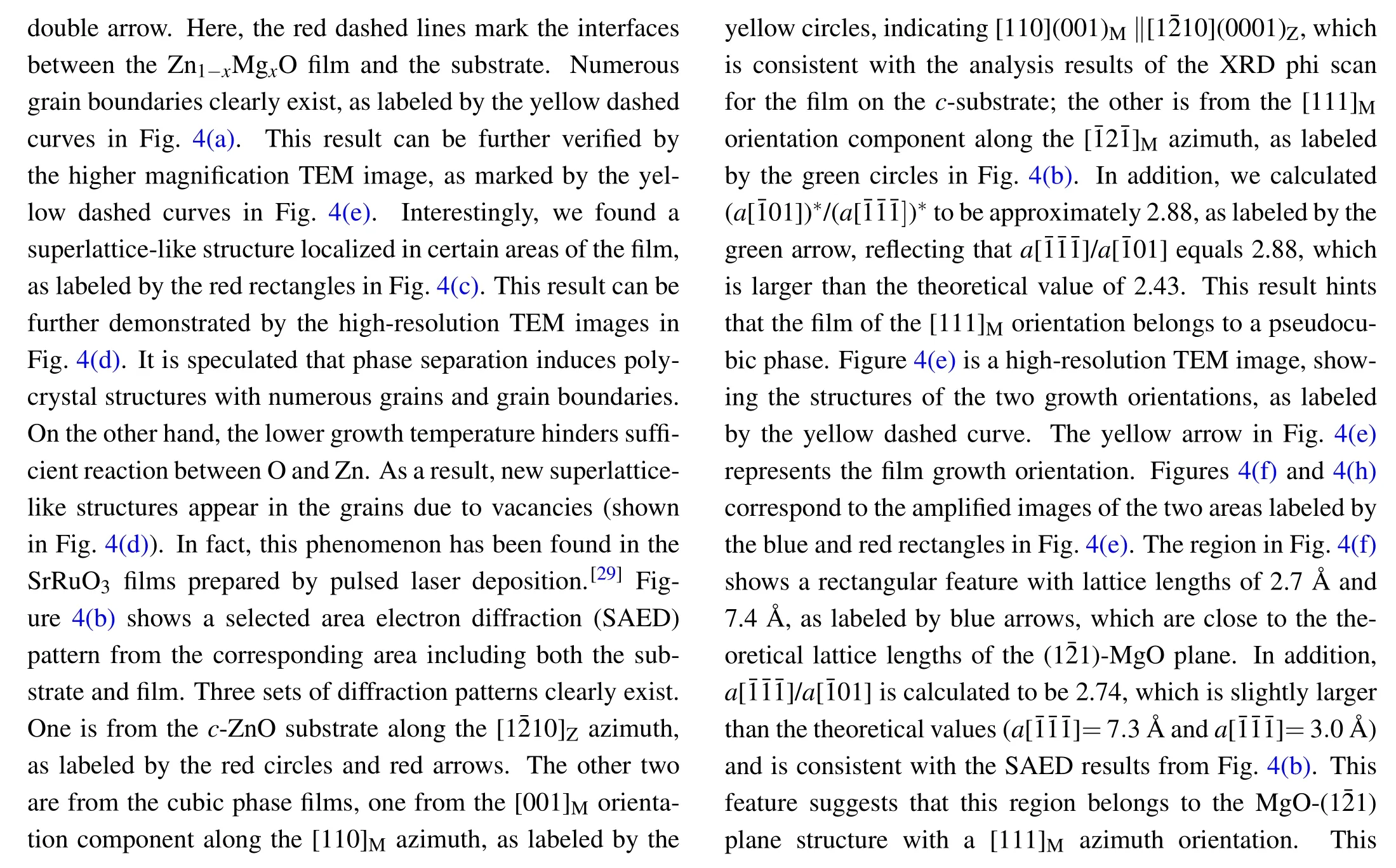

Fig.4.TEM image of the alloy film grown on the c-ZnO substrate:(a)low magnification TEM image;(b)the corresponding SAED;(c),(d)HRTEM images of the film,showing the superlattice-like structure in some areas,as marked by the red rectangle in image(c)and the yellow circle in image(d);(e)HRTEM image showing two regions separated by the yellow dashed line.(f),(h)The corresponding enlarged images of the two areas marked by the blue and red rectangles in(e);and(g),(i)the corresponding FFT images from(f),(h).
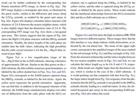

Fig.5.TEM images of the alloy film grown on the m-ZnO substrate:(a)low magnification image of the film on the m-ZnO substrate.(b)Corresponding SAED of(a).(c),(d)HRTEM images of two different areas.The illustrations in the upper right corners of(c),(d)correspond to the enlarged image of the area,as shown by the red and blue rectangles in(c)and(d),respectively.(e),(f)Two different areas grown on the m-ZnO substrate.The HRTEM image of the thin film shows many grain boundaries,which are indicated by the yellow dashed curves.
5.Conclusion
Acknowledgement
We are grateful to the members of the MBE laboratory of the Department of Physics,Xiamen University for their help and discussion.
杂志排行

Chinese Physics B的其它文章
- Multiple solutions and hysteresis in the flows driven by surface with antisymmetric velocity profile∗
- Magnetization relaxation of uniaxial anisotropic ferromagnetic particles with linear reaction dynamics driven by DC/AC magnetic field∗
- Influences of spin–orbit interaction on quantum speed limit and entanglement of spin qubits in coupled quantum dots
- Quantum multicast schemes of different quantum states via non-maximally entangled channels with multiparty involvement∗
- Magnetic and electronic properties of two-dimensional metal-organic frameworks TM3(C2NH)12*
- Preparation of a two-state mixture of ultracold fermionic atoms with balanced population subject to the unstable magnetic field∗