Vertical WS2 spin valve with Ohmic property based on Fe3GeTe2 electrodes∗
2021-09-28CeHu胡策FaguangYan闫法光YucaiLi李予才andKaiyouWang王开友
Ce Hu(胡策)Faguang Yan(闫法光)Yucai Li(李予才)and Kaiyou Wang(王开友)
1State Key Laboratory of Superlattices and Microstructures,Institute of Semiconductors,Chinese Academy of Sciences,Beijing 100083,China
2Center of Materials Science and Optoelectronics Engineering,University of Chinese Academy of Sciences,Beijing 100049,China
3Beijing Academy of Quantum Information Sciences,Beijing 100193,China
Keywords:WS2,Fe3GeTe2,spin valve effect,Ohmic property
1.Introduction
Two-dimensional(2D)transition-metal dichalcogenides(TMDCs)and their heterostructures have been regarded as a fertile ground for fundamental scientific research and technology application development in the field of solid-state physics.[1,2]Compared with thousands of studies in electronics and optoelectronics,experimental investigations of spintronics based on TMDCs are rare.[3–6]The basic challenge is that the traditional methods to prepare TMDCs-based magnetic heterostructures hinder the acquisition of high-quality electronic interfaces between covalently bonded magnetic materials and ultra-thin van der Waals(vdW)TMDCs layers,which is crucial for spintronic heterostructure devices.[7,8]Encouragingly,the recent discovery of layered magnetic materials could help to overcome this basic challenge.[9–13]The artificial vdW stacking TMDCs-based all-2D magnetic heterostructure in an inert environment through a transferstacking method can not only ensure the high-quality interfaces assembled by pristine 2D crystals without degradation,but also avoid the common obstacles in traditional magnetic heterostructure growth such as lattice mismatch and atom interdiffusion.[14,15]
As one of the most studied heterostructure devices in spintronics,vertical spin valve devices are normally composed of two ferromagnetic metals separated by a non-magnetic spacer,[16–20]except for the recent reported spin valve devices using layered ferromagnets without any spacer layer.[21]Despite that there are many reports on the magnetoresistance(MR)effect of spin valve devices with 2D materials(such as graphene)as the nonmagnetic spacer layer,the semiconducting TMDCs-based spin valve remains a relatively unexplored area.[7,22–29]In addition,as distinct from the tunneling spin valve,the low contact resistance and bias-independent MR make the spin valve with Ohmic property more suitable for practical spintronic applications that require stable device performance.[30]Therefore,the TMDCs-based all-2D spin valve with Ohmic property is highly desirable.
Here,we experimentally realized all-2D vertical spin valve devices based on vdW heterostructures comprising of a thin semiconducting WS2flake acting as a spacer layer and two exfoliated metallic Fe3GeTe2(FGT)flakes acting as ferromagnetic electrodes.Owing to the influence of the interface hybridization between the ferromagnetic metal FGT and the semiconductor WS2,we observed Ohmic properties and metallic rather than nonlinear transport behaviors of our FGT/WS2/FGT spin valve devices.The MR measurements demonstrate that our metallic vdW heterostructure devices have robust spin valve effect where the MR effects do not depend on the applied bias in the wide range of measurements.And the temperature evolution of the MR effect follows the Bloch’s law.
2.Experimental details
Device fabricationThe FGT,WS2,and hexagonal boron nitride(h-BN)(all from HQ Graphene)flakes were mechanically exfoliated inside a nitrogen filled glove box with oxygen and water contents lower than one part-per-million(ppm).Pre-patterned Cr/Au(5/45 nm)electrodes were prepared on Si substrates with 300 nm thickness SiO2layer by photolithography,magnetic sputter deposition,and lift-off.Thereafter,vertical FGT/WS2/FGT/h-BN heterostructures were sequentially transferred and stacked carefully by employing a dry-transferstacking method in the glove box.Finally,devices were annealed at 120°C for 10 min in the glove box to eliminate the possible bubbles and ensure closer stacking between the layers,and were stored inside until the devices were loaded into a low temperature probe station.
CharacterizationsThe magnetotransport measurements were carried out in a cryostat(Lake Shore Cryotronics,Inc)with a base temperature of 10 K and a 2.25 T superconducting magnet.TheI–Vcurves and spin valve effect were measured by using the combination of a Keithley 2602B SourceMeter and a Keithley 2182A Nanovoltmeter.Note that the positive current direction is defined as the current flow from the top FGT layer to the bottom FGT layer for all devices.
3.Results and discussion
Figure 1(a)shows the schematic diagram of the twoterminal vertical spin valve device,which comprises of two metallic FGT ferromagnetic electrodes separated by a semiconducting WS2spacer layer and a top h-BN capping layer.Ultra-thin WS2flakes with thickness around 5 nm were used to ensure that the spin polarization of the electron would not be completely scattered when it passes through the WS2spacer.The multi-layer FGT flakes with thicknesses exceed 10 nm,which remain a 3D magnetic characteristic,were employed as the ferromagnetic electrodes to guarantee a strong perpendicular magnetic anisotropy and a similar interfacial hybridization strength.[31]The heterostructures were encapsulated with top h-BN layers(typically 20–30 nm)to prevent degradation once exposed to air.Figure 1(b)shows the optical micrograph of the device used to measure the data presented in the main text.The details of the device fabrications and characterizations were given in Section 2.Atomic force microscope(AFM)was applied for the characterization of the device(Fig.S1a).The thicknesses of the layers for a typical vertical heterostructure device were measured as(see Fig.S1b for the height profiles):13.2 FGT/6.5 WS2/16.1 FGT/30 h-BN(from bottom to top,in nm).
We first investigated the electrical transport properties of the vertical FGT/WS2/FGT heterostructure devices from 10 K up to 240 K(above the Curie temperature of FGT),by measuring the current–voltage(I–V)curves and studying the temperature evolution of the junction resistance(RJunction–T).Prior to any charge transport measurements,we first applied a large magnetic field of 0.5 T to ensure the bottom and the top FGT ferromagnetic electrodes in parallel configuration.Figure 2(a)shows that theI–Vcurves remain linear at various measured temperatures for both below and above the Curie temperature of FGT,indicating the Ohmic characteristic of the heterostructure device.Moreover,the correspondingRJunction–Tcurve in Fig.2(b)clearly shows that theRJunctiondecreases monotonically with decreasing the temperature down to 10 K,revealing the metallic transport behavior of the heterostructure in spite of the semiconducting nature of the WS2spacer.Both the linearI–Vcharacteristic and metallicRJunction–Tbehavior imply the metallic interface rather than the Schottky barriers formed between the WS2and the two FGT ferromagnetic electrodes.This is a common behavior of thin semiconductors(such as MoS2and WSe2)sandwiched by ferromagnetic electrodes(such as permalloy and FGT),which originates from the intense hybridization at or in the vicinity of the interfaces.[7,24,26,28]
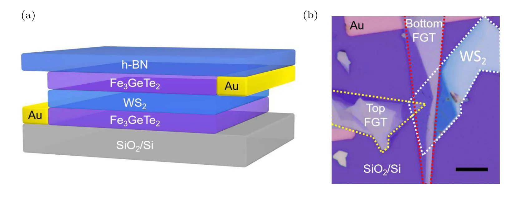
Fig.1.Device fabrications.(a)Schematic of the FGT/WS2/FGT vdW heterostructure device,with top h-BN passivation.(b)Optical micrograph of the device used to measure the data presented in the main text(scale bar,10µm).

Fig.2.Magnetotransport properties of the FGT/WS2/FGT device.(a)I–V curves at different temperatures,showing the linear characteristics.Inset is the zoom-in view.(b)Resistance of the heterostructure as a function of the temperature(RJunction–T).RJunction increases with rising temperature in the measurement range 10 K to 240 K,exhibiting a metallic behavior.(c)Hysteresis of the device resistance as a function of the perpendicular magnetic field(RJunction–B)at a fixed current bias of 5µA.Black and blue horizontal arrows represent the sweeping directions of the magnetic field.
Having known the mechanism of the vertical transport of the WS2-based heterostructure devices,we then investigated the spin valve effects by measuring theRJunctionas a function of the perpendicular magnetic field(RJunction–B)at a particular bias current(5µA,unless otherwise specified).Figure 2(c)shows theRJunction–Bcurves at 10 K,displaying typical spin valve effects with two resistance states.When the magnetic field is swept from negative to positive(blue curves),sharp transition to the high resistance state is observed when the field is close to 0.17 T(corresponding to the antiparallel magnetization alignments↓↑or↑↓,where the arrow represents the out of plane magnetization of the FGT ferromagnetic electrode),and then falls back to the low resistance state(corresponding to the parallel magnetization alignments↓↓or↑↑)at a slightly larger field of around 0.20 T.When the magnetic field is swept back to negative(black curves),the resistance has corresponding symmetric up and down transition.The magnitude of the associated magnetoresistance(MR)can be defined by(RAP–RP)/RP,whereRAPandRPare the resistances at antiparallel and parallel magnetic configurations of the two FGT ferromagnetic electrodes,respectively.The MR is obtained to be 0.45% at 10 K.If we assume the top and bottom FGT ferromagnetic electrodes have the same electron spin polarizationP,the MR can be approximated as MR=2P2/(1−P2),which is deduced from the modified Julliere’s model.[7]Then,the spin polarization of the FGT electrodes is calculated to be~5%.
Figure 3(a)shows theI–Vcurves measured at 10 K in the parallel and antiparallel magnetization alignment under zero magnetic field.The slightly different slopes of the two linearI–Vcurves demonstrate the nonvolatile characteristic of the two different magnetic configurations.We further investigated the temperature dependence of the spin valve effect.Figure 3 shows the MR curves measured at various temperatures.With increasing the temperature,the magnitude of the MR decreases and vanishes above the Curie temperature at about 220 K,as shown in Figs.3(b)and 3(c).The reduction of the MR at higher temperatures can be caused by two reasons:one is that the thermal fluctuation strengthens with rising the temperature,and the other is that the spin polarization is proportional to the magnetization and decreases with increasing temperature.Moreover,the critical magnetic switching field of the spin valve decreases with increasing the temperature[Fig.3(b)],which is attributed to the temperature dependence of the switching fields in the FGT flakes.The coercivity of FGT decreases with increasing the temperature,which is the result of the reduction of perpendicular anisotropic energy and the enhancement of thermal agitation energy.[31]The temperature evolution of the MR magnitude can be analyzed by Bloch’s law,where the spin polarization is described byP(T)=P0(1−αT3/2).Thus,by fitting the temperature dependence of the spin polarization,a material-dependent constantαcan be estimated to be 1.4×10⁻⁴K−3/2.This value is comparable to the reported value in the literature.[28]

Fig.3.Temperature-dependent spin valve effect of the FGT/WS2/FGT device.(a)I–V curves in parallel(P)and antiparallel(AP)magnetization alignment measured at 10 K under zero magnetic field.Inset is the zoom-in view.(b)MR curves at different temperatures.(c)MR magnitude and the corresponding spin polarization(P)as a function of temperature.The data is fitted to Bloch’s law(red line),yielding a material-dependent parameter α=1.4×10⁻⁴ K−3/2.
Next,we studied the bias current dependence of the MR effect at 10 K.As shown in Fig.4(a),the MR curve measured at a negative bias current of 5µA yields the value of 0.45%,which is equal to the value of the positive counterpart,implying that the device possesses perfect up-down symmetry and two identical high-quality FGT-WS2vdW interfaces.The physical mechanism of our spin valve devices is the spindependent scattering transport.Figure 4(b)shows the spin valve effect at various bias currents ranging from 100 nA to 50µA.As shown in Fig.4(c),owing to the Ohmic property of the WS2-based spin valve device,the MR magnitude stabilizes around 0.45%and does not depend on the bias current,which meets the demand in stable device performance for practical spintronic applications.This bias-independent MR behavior was also observed in the previous studies.[30]
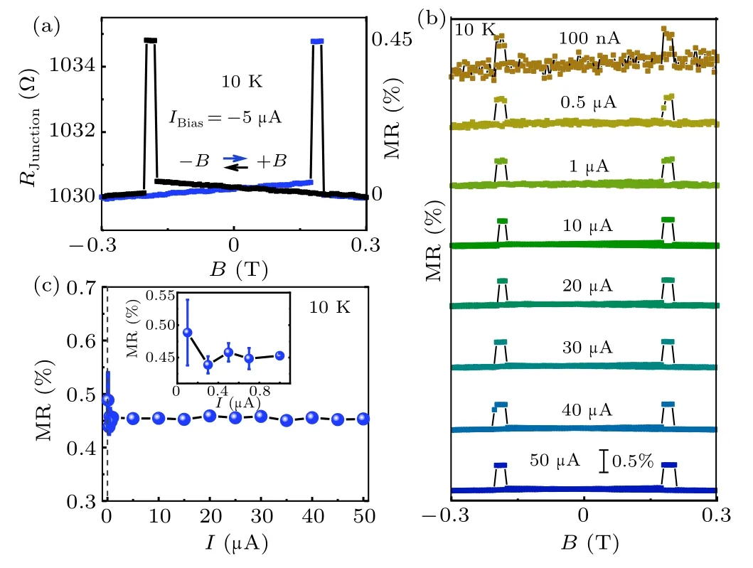
Fig.4.Bias-dependent spin valve effect.(a)MR curve measured at a negative bias current of 5µA.(b)MR curves at various bias currents ranging from 100 nA to 50µA.(c)MR magnitude as a function of bias current.Inset is the zoom-in view.
4.Conclusion
In summary,we have fabricated and investigated spin valve devices with high quality interfaces based on FGT/WS2/FGT vdW heterostructures.Interestingly,the unexpected Ohmic property and metallic rather than nonlinear transport behaviors were observed.This should be a universal phenomenon of ultrathin semiconductors sandwiched by ferromagnetic electrodes,which is related to the strong hybridization between the interface of WS2and FGT.Moreover,the magnetotransport measurements show that our WS2-based metallic heterostructure devices have robust spin valve effect,and its MR effects do not depend on the bias current due to the Ohmic property.The results of our work indicate that all-2D magnetic heterostructure,facilitated by combining 2D magnets,is expected to be a promising alternative for TMDCsbased spintronics,and may contribute a feasible spin valve structure for realistic applications that require stable device performance.
杂志排行
Chinese Physics B的其它文章
- Origin of anomalous enhancement of the absorption coefficient in a PN junction∗
- Protection of isolated and active regions in AlGaN/GaN HEMTs using selective laser annealing∗
- First-principles study of plasmons in doped graphene nanostructures∗
- Probing thermal properties of vanadium dioxide thin films by time-domain thermoreflectance without metal film∗
- An improved model of damage depth of shock-melted metal in microspall under triangular wave loading∗
- Signal-to-noise ratio of Raman signal measured by multichannel detectors∗