Low-power emerging memristive designs towards secure hardware systems for applications in internet of things
2021-07-28NanDuHeidemarieSchmidtIliaPolian
Nan Du ,Heidemarie Schmidt ,Ilia Polian
a Department Nano Device Technology,Fraunhofer Institute for Electronic Nano Systems,Technologie-Campus 3,09126,Chemnitz,Germany
b Faculty of Electrical Engineering and Information Technology,Chemnitz University of Technology(TU Chemnitz),Straße der Nationen 62,09126,Chemnitz,Germany
c Department of Quantum Detection,Leibniz Institute of Photonic Technology(IPHT),Albert-Einstein-Str.9,07745,Jena,Germany
d Institute for Solid State Physics,Friedrich Schiller University Jena,Fürstengraben 1,07743,Jena,Germany
e Institute of Computer Engineering and Computer Architecture(ITI),University of Stuttgart,Pfaffenwaldring 47,70569,Stuttgart,Germany
Keywords:Memristive technology Nanoelectronic device Low-power consumption Miniaturization Nonvolatility Reconfigurability In memory computing Artificial intelligence Hardware security primitives Machine learning-related attacks and defenses
ABSTRACT Emerging memristive devices offer enormous advantages for applications such as non-volatile memories and inmemory computing(IMC),but there is a rising interest in using memristive technologies for security applications in the era of internet of things(IoT).In this review article,for achieving secure hardware systems in IoT,lowpower design techniques based on emerging memristive technology for hardware security primitives/systems are presented.By reviewing the state-of-the-art in three highlighted memristive application areas,i.e.memristive non-volatile memory,memristive reconfigurable logic computing and memristive artificial intelligent computing,their application-level impacts on the novel implementations of secret key generation,crypto functions and machine learning attacks are explored,respectively.For the low-power security applications in IoT,it is essential to understand how to best realize cryptographic circuitry using memristive circuitries,and to assess the implications of memristive crypto implementations on security and to develop novel computing paradigms that will enhance their security.This review article aims to help researchers to explore security solutions,to analyze new possible threats and to develop corresponding protections for the secure hardware systems based on low-cost memristive circuit designs.
1.Introduction
Recent advances in energy-and cost-efficient computation and in cloud/wireless infrastructure have led to the Internet of Things(IoT)[1].The IoT has been a main driving factor in scientific,technological,economic and social progress.IoT comes with a set of requirements:ultra-low-power consumption for long-term autonomous operation without the possibility of recharging the battery;the need to function reliably in harsh environments;and the resilience against possible malicious cyber-attacks(including both:remote attacks mounted through network connections and physical attacks by adversaries[2]).Past spectacular cyber-attacks have clearly demonstrated the vulnerability of existing systems and the need to prevent such attacks in the future.
Modern cryptographic schemes are related to our daily lives.The majority of available cyber-defenses concentrate on protecting the software part of electronic systems or their communication interfaces.However,manufacturing technology advancements and the increasing hardware complexity provide a large number of challenges so that the focus of attackers has shifted towards the hardware level.In particular,we saw already evidence for powerful and successful hardware-level attacks that circumvent any software-level security mechanisms.
The attacks mentioned above happened on products built using stateof-the-art microelectronic technology, however, we are facing completely new security challenges due to the ongoing transition to radically new types of nano-electronic devices,such as memristors,spintronics,or carbon nanotubes.The use of such emerging nanotechnologies is inevitable to continue the exponential improvement of integration density and address the key challenges related to energy efficiency,computing power and performance.Therefore,the entire industry,from foundries to circuit and system designers,are switching to these emerging nano-electronics alongside scaled CMOS technologies in heterogeneous integrated systems.The progress in nanotechnology promises to address some of the aforementioned requirements/challenges for IoT:Power management,scalability,sustainability and reliability.For example,memristive technologies are considered as a hot candidate to complement or even replace traditional CMOS technology in applications from domains such as Internet of Things or autonomous systems.
The memristive technologies come with attractive properties,especially nonvolatility and reconfigurability,and also facilitate the development of non-volatile memory(Mem-NV memories)and in-memory computing architectures,i.e.memristive reconfigurable logic computing(Mem-Logic computing)and memristive artificial intelligent computing(Mem-AI computing)as demonstrated in Fig.1.The memristive technologies and architectures provide new opportunities for achieving security targets(e.g.,by realizing stateful cryptographic functions or neuromorphic anomaly-detection co-processors),but also raise questions about their vulnerabilities to new types of hardware-related attacks.
There are several review articles on specific memristive security primitives.For example[3],focuses exclusively on memristor oriented physical unclonable functions(PUFs)and[4]on memristor oriented PUFs and true random number generators(TRNGs),whereas[5]reviews memristor oriented chaotic systems and hash functions.Such review articles are generally introducing only one or two memristive implementations of cryptography systems.In comparison to that,our review article is aiming at a higher-level,application-oriented analysis of memritive security techniques,i.e.to explore the security implication by reviewing the major areas of memristive applications.This article reviews the hardware-oriented security for the applications in IoTs,with a particular focus to the impact of revolutionary emerging memristive applications on security.We start with an overview of the three emerging memristive application areas:Mem-NVmemories,Mem-logic computing,and Mem-AI computing,with a focus on their key differences from their non-memristive counterparts.Then,we introduce three emerging topics of hardware-oriented security where we can expect memristive solutions to unfold their full potential:
·Memristive entropy primitives that can be used,e.g.,for generation of secret keys;
·Memristive cryptographic functions,specifically block ciphers that can encrypt data and provide its confidentiality;
·Memristive machine-learning systems,which can be used to defend the system against attacks.
We will review state-of-the-art in novel secure system designs based on low-power memristive technology in IoT.This review article aims at showcasing the application-level features at the interdisciplinary frontier of material science and hardware security.Many security approaches are based on cryptographic schemes and primitives,and therefore we will have to brie fly introduce the basic mathematical concepts and state of the art developments for some of the modern cryptographic solutions,in a manner meant to be accessible for researchers from material science and electrical engineering.Thus this article can serve as a step stone for future researchers to understand the advantages and disadvantages of memristive devices in the world of security and cryptography.
The remainder of this article is organized as follows.Wefirst introduce the background of memristive applications regarding three major areas:NV(nonvolatile)memory,reconfigurable logics and artificial intelligent computing(section 2).In the following sections 3 to 5,the three emerging hardware security topics mentioned above are reviewed.It has to be understood that any categorization of a developing scientific topic has its limitations,as some research questions cannot be perfectly attributed to a single sub-area of hardware-oriented security.Thus in the end of each section,the prospective/expected impact of memristive technology both on respective and extended implementation designs will be discussed.Moreover,we discuss the potential security vulnerabilities associated with memristive technologies in Section 6.
1.1.Background on memristive applications and hardware security
IoT demands dedicated secure chips with constrained power consumption.The power optimization on all levels of design abstraction is the key point,and is also helpful for increasing the chip reliability and chip life.In-memory-computing(IMC)is one of the leading solutions to realize area-and energy-constrained hardware systems for IoT security applications.

Fig.1.Memristive applications and their connections to secure hardware systems for applications in Internet of Things(IoTs).
As demonstrated in Fig.2,the separation between processing units and data storage units has been considered as the basic assumption for designing computing architecture,i.e.von-Neumann architecture(Fig.2a).Orders of magnitude improvement in computer performance has been achieved by the impressive technological achievements in these two essential system units(processor speed up,reduced power consumption and the downscale of system dimensions).As nowadays both processing and data storage units have reached a scaling barrier,the processing performance is now limited mostly by the inevitable need for data transferring[6],the so-called memory wall.To alleviate the memory wall,numerous approaches have been developed,including integration of cache memory near to processor[7]or integration of processing units within memory unit[8–10].However,the data transfer between processing and memory units are not fully eliminated within these approaches.Memristive technology can fully explore the potential benefits of IMC,with which the data transfer is reduced by adding processing capabilities into the memory itself(Fig.2b).Furthermore,for the essential building blocks,i.e.logic gate in Mem-Logic computing scheme and the artificial synapse in Mem-AI computing scheme can be realized more efficiently by exploiting the memristive devices[11,12].Such building blocks that realized with less numbers of memristive devices lead to further less power and less connections(i.e.more space between connections),where the system reliability is thus enhanced.
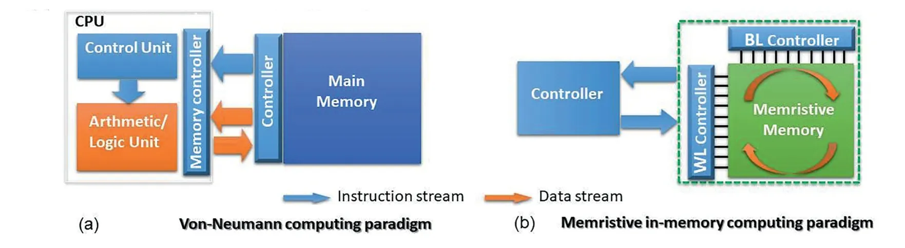
Fig.2.General structures of(a)CMOS-based von-Neumann computing paradigm and(b)memristive in-memory computing paradigm.
1.2.Introduction to memristive devices
Memristive devices have been investigated intensively since the link between memristor theory by L.Chua[13]and physical resistive switching device was established by HP labs in 2008[14].A memristor is a two-terminal device,whose resistance can be modulated by applying appropriate electrical stimuli.The programmed resistance states,i.e.low resistance state(LRS)and high resistance state(HRS),are in general non-volatile.The“SET”process is usually referred to a switching procedure from HRS to LRS,while the“RESET”process is a switching procedure from LRS to HRS.Over past decades,the resistive switching(RS)behaviors were found in various materials:phase-change chalcogenides[15,16],solid-state electrolytes[17],organicfilms[18,19],and transition metal oxides[20–22].Several physical representations have been established correspondingly for resolving resistive switching behavior in memristive devices,for example,the switching behavior can be induced by a Joule heating induced phase change mechanism(PCM memories)[23],by switching the magnetization in magnetic tunnel junctions(MTJs)with spin-polarized currents[24],by electric-field induced switching of the ferroelectric polarization in ferroelectric tunnel junctions(FTJs)[25],or by electric-field induced ionic motion and concurrent redox reactions(ReRAMs)[26].
In general,one can distinguish between memristive devices predominantly switching between two states or multiple states.If the memristive device switches quite abruptly between a HRS and a LRS,we will call such devices digital memristive devices.Other devices have a very smooth transition between different states enabling an analog tuning of the resistance state,which can be called analog memristive devices.One material system could possess different RS behavior depending on the electrode material,oxide properties(thickness,bandgap,and trap energy level),interfacial barrier height between metal and oxide,and fabrication process(deposition technology,annealing temperature and ambient).Here we take VCM(valence change memory)ReRAM as an example.The VCM devices have attracted much attention and offer a promising opportunity for constructing the IMC paradigm,due to their excellent potential performances,such as non-volatility,low power consumption[27],excellent scalability[28],fast switching speed[29]and high endurance and retention[30].The switching mechanism of VCM devices are related with the ionic motion of oxygen defects and concurrent redox reactions in a transition metal oxide in a metal/-oxide/metal stack.
The VCMReRAMs can show digital or analog switching behavior.The RS in digital VCM devices involves construction and rupture of conductivefilaments through the oxide layer(filamentary switching)[31,32].As shown in Fig.3a,thefilaments,which are acting as“bridges”,extend from one electrode to the other one for charge transport throughout transition metal oxide layer.The effective Joule heating associated with a localized conductionfilament enables fast ion motion during switching.Thus the current in LRS flows through the confined local path,and the resistance in LRS is independent of electrode area size.By an application of a certain voltage pulse the conductionfilament is ruptured and the device can be switched back to HRS,where the resistance in HRS increases with decreasing cell size[33].One critical and yet potentially problematic step for the initial formation process of the conductingfilament in digital VCM devices is electroforming(as shown in inset of Fig.3a),i.e.,a one-time application of stronger electricfield strength upon device operation,i.e.a much-higher voltage than used during regular switching processes.In general,thefilamentary switching devices can only be functioning after performing electroforming process;it has to be accepted that the induced maximum current can damage or destroy the device through thermodynamic dielectric breakdown,leading to yield loss or deteriorated long-term reliability.For this reason,there is a substantial interest in the usage of analog switching memristive devices for avoiding the electroforming step altogether.For instance,BiFeO3(BFO)memristive device[34,35]is belonging to the catalog of electroforming-free analog memristive devices.Their further advantage is their self-rectifying behavior,which is key for developing selector-free memristive crossbar arrays(MCAs),because it can effectively eliminate the sneak current when the cells are organized in a crossbar architecture with no need for a diode or transistor for each cell in the crossbar structure.
The RS in analog VCMdevices in general results from the modulation of carrier transport barrier at the electrode/switching layer interface induced by ion migration(interfacial switching)[36,37].Upon an application of a positive or negative electric stimulus,oxygen vacancies in oxide layer can drift toward or rejected from the electrode/oxide interface(Fig.3b),and the local charge carrier concentration near the interface can be changed,which modulates the interfacial barrier height or depletion layer thickness at the interface between oxide layer and TE/BE and leads to the modulation of the transport properties.
As aforementioned,bothfilamentary digital switching and interfacial analog switching in VCM devices are induced by ion migration,but the transition oxide layer does not contribute to the switching in interfacial switching,and is considered leaky compared to thefilamentary switching.Therefore,the resistance state can be exclusively dominated by the interfacial effect in interfacial switching,whereas the transport process infilamentary switching is controlled by local conductionfilaments.Furthermore,the retention time limitation in interfacial switching VCM devices might be caused by the migration of oxygen vacancies under low electricfield in the long time domain[38].

Fig.3.Schematics of switching mechanisms using different classification criteria:(a)Filamentary switching(inset shows sketch before electroforming process)and(b)Interfacial switching.

Fig.4.Relationship between memristive switching properties,memristive applications and hardware security for IoT.
To further enhance the memristive device performance,i.e.data retention property or power consumption,it is crucial to identify the exact physical transport mechanism and its relation with resistive switching phenomena.For example,the switching velocity will in fluence the energy cost of RS behavior.The resistive switching material tends to have higher density of traps,which allows electrons/ions to hop from one to another traps with lower cost.Furthermore,especially,to assess the memristive devices with lower power consumption,the required voltage or current level of switching procedure plays an important role(it makes a difference whether SET or RESET processes are considered).In analog VCM devices,the reduction of power consumption can be realized by shrinking the contact size,whereas in digital VCM devices,it can be fulfilled by reducing the length or radius offilamentary conduction path in LRS.As experimentally observed in niobium oxide VCM devices[27],the SET process can be fulfilled at sub-nanosecond times and~100 fJ energies with 30 nm radius of conduction path.Such energy dissipation is expected to be depressed down to tens of fJ at tens of ps switching time with 10 nm radius.
1.3.Introduction to memristive applications
The memristive devices attract much attention due to their excellent potential performances as demonstrated in Fig.4.Nonvolatility1Memristor discussed in the paper must be nonvolatile,the volatile diffusive memristors[39]in some of publications are not included here.and variability are the two intrinsic properties of memristive devices,which are shared among all types of memristive devices.Retention and endurance[30]are the two functional switching properties,which define the life time of the constructed secure primitives introduced in the review paper.The other preferable properties of memristive devices are low-power consumption[27],excellent scalability[28],fast switching speed[29],large off/on ratio[40],high uniform switching[41],and multi-level switching[42].
There is currently no“perfect”memristive device that combines all the desirable properties as listed in Fig.4.For example,analog switching memristive devices show higher uniformity than digital switching devices,but require higher switching voltages,i.e.higher power consumption.In contrast,digital switching memristive devices often require an electroforming step while analog memristive devices are typically electroforming-free.Therefore,the choice of the memristive device for a practical system within a given application context must be guided byfitness of its functional properties(such as analog vs.digital switching dynamics,endurance,retention).In the following sections we will demonstrate unconventional ways to construct secure systems by exploiting emerging memristive devices.Their functional properties pave the way to obtain secure systems that outperform their conventional CMOS counterparts,especially in terms of area-and power-consumption for the IoT applications.For this purpose three major memristive applications,i.e.Mem-NV memories,Mem-Logic computing,and Mem-AI computing,are reviewed.
1.3.1.Mem-NV memory by exploiting memristive technology
The initial interest in memristive applications was due to their outstanding nonvolatile properties in constructing the non-volatile memories[43–46].Memristive memories(ReRAMs)have already led to early commercial products[47–49],and memristors are likely to play a leading role in next generation low power and high-density memory systems[50].Such NVMs can be further used for entropy primitives for key generation due to the intrinsic properties of memristive devices,i.e.nonvolatility and variability.
1.3.2.Mem-Logic computing by exploiting memristive technology
Reconfigurable memristive devices provide logical building blocks[51,52]for designing innovative in-memory computing paradigms[53].Several logic families are realized by exploiting emerging memristive devices,and the circuit designs of representative logic gates for different logic families are demonstrated in Fig.5.The popular representatives for stateful logic concept are memristor-based material implication(IMPLY)logic[54]and memristor-aided logic(MAGIC)[55],which are attractive for IMC with memristance as input and output logic state variable.The universal logic gate set in MAGIC logic family can be realized by using sequential operation of NOR gate,whereas in IMPLY logic family the IMP and FALSE logic gates are needed.The typical lengthy sequence operation and possible difficulties in cascading multiple memristive gates[55]are major problems in possible applications.The memristor ratioed logic(MRL)[56]that provides efficient AND and OR functionality and leads to low latency implementations[57]but requires CMOS inverters in order to obtain a universal gate set.By applying sequential logic concept,the complementary resistive switching based logic(CRS)[58]and CRS with non-destructive reading(CRS-R)[11]are able to realize the logic functions by using only single one memristive device,especially the CRS-R logic was developed based on the BiBFO EF-free memristors[11]with potential of low area cost.The difference between CRS-R and CRS are the reading ability of the memristive cells,whether the output state needs to be read out to fulfill the truth table or not.Furthermore,the parallel input processing memristor(PIPM)[59]and the CMOS like logic[60](not shown in Fig.5)are strongly correlated with the memristive topology,which might have the high consumption of area and power,respectively(The CMOS like logic is also not possible for cascading logic).There are many review papers which introduce the operational details for each memristive logic family[61,62],and we will not list up all details here.Theoretically the same secure system can be constructed by all types of memristive logic families.The optimized choice of memristive logic concept is made by the application-level system requirements,especially on area size and latency.
1.3.3.Mem-AI computing by exploiting memristive technology
Artificial intelligence(AI)computing is high parallelism computing which can mimic the human intelligence by sensing,acting and adapting using artificial neurons and artificial synapses[63].AI computing can be used in potential areas in IoT,such as autonomous driving,image classification,object detection and localization,cancer detection,and natural language processing.
Attracted by the fascinating potential of AI computing paradigm,great efforts are enforced to develop various methods and algorithms for enabling artificial neural networks.During the past decade,leveraging memristive crossbar arrays(MCAs)for this purpose was proposed/reviewed by several dedicated review papers[67–69].The advantages of artificial neural networks implemented by MCAs in comparison to their counterparts based on the traditional CMOS technology,e.g.,CMOS-basedfield-programmable gate array(FPGA)[70],can be summarized as follows:
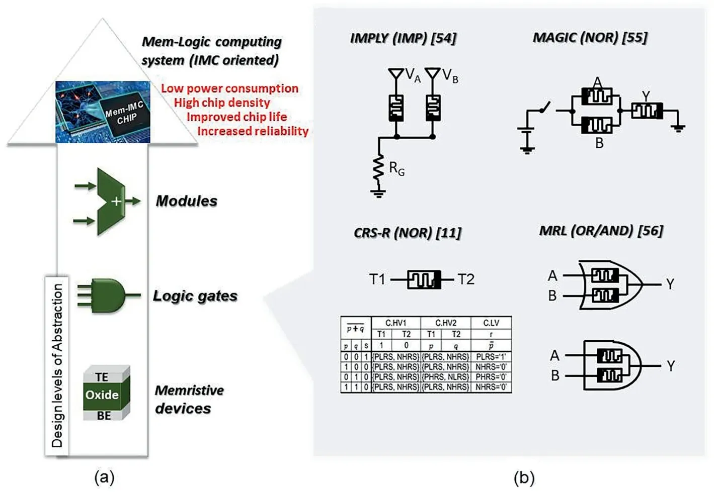
Fig.5.Mem-Logic computing application.(a)Demonstration of design levels of abstraction for Mem-logic computing application.(b)Realization of representative Boolean logic building blocks by utilizing memristive IMPLY[54],MAGIC[55],CRS-R[11],MRL[56]logic families.The diagrams are adapted from the corresponding references.

Fig.6.Mem-AI computing application.(a)Demonstration of biological neural network with biological STDP.The biological diagram is adapted from Ref.[64].(b)Schematic demonstration of artificial neural network.(c)Demonstration of memristive artificial neural network,where the matrix-vector multiplication are computed by memristive crossbar array(MCA).(d)Illustration of STDP diagrams recorded from memristive artificial synapses based on HafOx[65],TaOy[66],and BFO[42]memristive devices.The copy right permission is available for Fig.6d.
·Reconfigurability of MCAs:A memristive cell is capable of realizing functions that need several transistors in a CMOS circuit[71]due to its intrinsic reconfigurability.Further due to its memory function with nonvolatility,no refresh of memristive state is needed even if the chip is powered off completely[72].Especially MCAs with analog memristive cells provide the possibility to process the analog sensory data directly in analog MCAs in analog domain without analog to digital conversion,which enables the reduction of circuitry complexity and depresses power consumption.
·Artificial synaptic behavior of MCAs:By drawing inspiration from the biology of the human brain(Fig.6a),the artificial neural network(Fig.6b)is constructed by exploiting the artificial neurons and artificial synapses,and the memristors have been employed as biorealisitc synaptic connection elements or neuron elements as demonstrated in Fig.6c.It has been observed that one single memristive cell with its nonvolatile dynamical behavior can intrinsically behave as an artificial synapse and mimic the learning rule of biological synapse[73,74](as shown in Fig.2d).In comparison,it would take several transistors in the traditional CMOS technology to emulate the same artificial synapse[75].Thus by using MCAs for AI data processing the scalability of circuit design can be greatly improved(Fig.6c).
·Parallel processing capability of MCAs:Matrix-vector multiplication is the key operation for artificial neural network algorithms,which dominates the computation time and energy consumption for many workloads.As illustrated in Fig.6c,in MCA,by applying a vector of voltage signals to the rows of a MCA,multiplication by each memristive cell's conductance is carried out by the Kirchhoff's current law and the current is summed across each column.Hence,an MCA can physically carry out vector-matrix multiplication in a single constanttime step[76].Such“analog”method of vector-matrix multiplication with high parallelism can be orders of magnitude more efficient than a digital circuit[77],particularly as the crossbar array size is highly scalable.The emerging MCAs can thus provide a promising hardware realization of artificial neural networks,which can,in the security context,be further utilized for both:machine-learning-based attacks and defenses.Fig.6d demonstrates different types of memristive devices can mimic the spike timing dependent plasticity(STDP)behavior of biological synapse.
Machine learning is one subset of AI computing that realized with algorithms and statistical models whose performance is improved at tasks with experience data.In this review paper,we focus on the machine learning implementations,because ML related hardware security issues has become one of the research emphases for the near future.
1.4.Hardware security
Today's electronic products are complex cyber-physical systems which integrate computing,their environment,sensors and actuators,networks(including the Internet),and their human users[78].Hardware is an essential part of these systems,and it can be both:a“root of trust”,which provides the fundament for their security,and their“Achilles'heel”that gives rise to new security loopholes.Hardware security is an emerging scientific discipline which studies both:hardware-related threats to security of electronic systems,and hardware-based approaches to protecting such systems against attacks.Security analysis usually assumes an intelligent,strategically-thinking attacker who can identify a system's“weakest link”and mounts an attack through it,and therefore strong security primitives and a secure realization and integration of hardware modules are needed.In the past,security research mostly concentrated on possible vulnerabilities related to a system's software and/or connectivity,while its hardware was traditionally assumed to be secure;this assumption is collapsing now.One reason for growing security concerns with respect to hardware is the better availability of equipment for measuring hardware or meddling with it(through probing,side-channel analysis,fault injection,circuit editing,etc.)to potential attackers.A second reason is the complex and distributed process of hardware design and manufacturing,where some of the involved parties might not be trustworthy.
Security aspects of hardware are strongly affected by the technological progress,both on technology and on architecture level.For example,larger integration densities of conventional CMOS technologies have led to proliferation of multi-core and many-core architectures,which in turn had a lasting impact on many areas of Computer Science and our daily lives[79].More importantly in the context of this survey,radically new devices,such as memristors,give rise to novel neuro-inspired[80],memory-centric[81]or approximate[82]computer architectures that can revolutionize computationally challenging tasks of today and tomorrow.Security implications of such novel architectures are only partially explored so far(an overview can be found in Ref.[83]).
In the following of this article,we focus on the role of memristive technologies in this context.Security aspects of the memristive devices,circuits and systems on their basis will be explored.Memristive technologies with their low energy and area consumption can lead to conceptually novel and strong security primitives,which can be leveraged to address hardware security problems and open the door for new applications.As mentioned in the introduction,we will consider three specific areas:entropy primitives;ciphers;and machine-learning functionality.
2.From intrinsic memristive properties towards entropy primitives
Emerging memristive devices with the inherent variability of their electrical parameters(e.g.,due to unpredictable manufacturing-induced changes in their sizes and dopant concentrations)are a natural entropy source for true random number generators(TRNGs),physical unclonable functions(PUFs)and other primitives from this section,for the purpose of secret generation for fundamental security functions including keybased encryption,authentication and identification.
“Entropy”is an information-theoretical concept that can be understood as measure of information provided by an observation,or amount of uncertainty before that observation.The main role of entropy in the security context is the generation of secrets,in particular secret keys for encrypting data.For instance,consider a blockBfor generating a 128-bit secret key;assume thatBis securely stored within an integrated circuit and an attacker,who is interested in learning(or obtaining)the key cannot directly read outB's outputs.If we assume thatBimplements(by some physical principle)a perfect coin toss,i.e.,each of the generated 128 bits is‘0’or‘1’with 50%probability and its value is independent of the other bits,then the resulting secret key is completely random and can assume any of 2128combinations.An attacker who wishes to guess this key would have to try all 2128possibilities,which is infeasible;this realization ofBhas a maximal entropy of 1 per bit,or 128 for the entire key.In contrast,blockB′that always produces a‘0’for each bit will result in a key that is not secure at all:It will always be a sequence of 128 bits‘0’,and the attacker will guess it immediately.The entropy of the key produced by blockB′is minimal,or‘0’.We can imagine further variants,e.g.,blockB’’that obtains the veryfirst bit by a coin toss,but all subsequent bits are just copies of thefirst bit.Here,there are two possible keys(all-‘0’and all-‘1’),and the entropy will be higher than‘0’but lower than 128.
2.1.Classical entropy primitives
The hardware primitive that implements the above-mentioned functionality and produces bits with as high entropy as possible is called a(true)random number generatoror TRNG[84].A modern TRNGconsists of anentropy source(a“sufficiently random”stochastic process)and post-processing circuitry.The entropy source can be off-chip,e.g.,a chamber with a radioactive substance and a detector producing detection events after unpredictable amounts of time,connected to an input of the actual TRNG.Of more relevance are TRNGs where the entropy sources are integrated into the primitive itself.A simple realization of an on-chip entropy source in conventional CMOS is aring oscillator,i.e.,a chain of an odd number of inverters where the output of an inverter is connected to the input of the next inverter and the output of the last inverter is connected to the input of thefirst inverter.This structure will oscillate between the digital values‘0’and‘1’with a high frequency;waiting for a sufficiently long time and reading out the output of the last inverter will result in a(somewhat)unpredictable outcome,because the delay of each inverter is slightly different due to process variability,voltage noise,temperature,crosstalk with neighboring logic,and other factors.An overview of advanced ring-oscillator-based TRNGs can be found in Ref.[85].
In general,the entropy source may not deliver perfect entropy due tobiases(more produced‘1's than‘0's or vice versa)orcorrelationsbetween bits.To obtain better entropy,post-processing is applied.Moreover,a TRNG for use in secure systems should fulfill certain further requirements,e.g.,the post-processing must not allow an attacker who managed to learn(compromise)one generated key to deduct the next or the previous key produced by the same TRNG(forward/backward secrecy).Modern TRNG security standards[86]also demand for a number ofself-testsintegrated into the TRNG.
Physical unclonable functions,or PUFs[87],are a second large class of entropy primitives considered today.A PUF is a“digitalfingerprint”of a circuit(or a different physical object)based on its inherentphysical disorder.Circuit-based PUFs typically use unpredictable variability in values such as delays,currents or voltage levels as the source of entropy.For example,an SRAM PUF is simply an array of static random-access memory cells;the value produced by this PUF is the vector of logical values(‘0’or‘1’)to which these cells initialize after being switched on.Due to slight fabrication-induced asymmetries within the memory elements,this vector will be different for different manufactured instances of the same circuit and can therefore serve as itsfingerprint.Thisfingerprint can serve as the unique identifier of the circuit's specific manufactured instance.In contrast to generating the unique identifier off-chip and storing it in an on-chip non-volatile memory,a PUF is an intrinsic feature of an individual circuit.
Similar to TRNGs,PUFs can be used for secret key generation(and have further applications in so-called challenge-response authentication protocols).However,there is an important difference:A TRNG aims at extracting a bit sequence with a maximum entropy per bit from thesameobject,whereas a PUF extracts maximum entropy from apopulationof manufactured objects.In other words,running the same TRNG multiple times will result in different responses,whereas running the same PUF multiple times should result in the same response,but this response will be different for different copies of the same circuit(this property of a PUF is calleduniqueness).In fact,reliability(the probability to generate a stable response even under varying temperature and voltage noise)is a central requirement for a good PUF,especially if it will be used for generating cryptographic keys where even one flipped bit leads to completely distorted ciphertexts.Many PUFs do not guarantee perfect reliability(for example,an SRAM PUF may include unstable cells that are sometimes initialized to‘1’and sometimes to‘0’),and error-correction or fuzzyextraction postprocessing is applied to them[88,89].
2.2.Memristive entropy primitives
We will focus on two entropy primitives from the domain of hardware-oriented security(TRNG and PUF).Below,we summarize representative memristive realizations and their requirements.
A TRNG should have good statistical properties(e.g.,lack of bias or autocorrelations)and also good security properties(forward and backward secrecy,i.e.,difficulty to guess the TRNG's next or previous outputs from its current output)[90]as demonstrated in Fig.7a.Thefirst memristive TRNG(M-TRNG)was suggested in 2010[91].Several M-TRNGs exploited random telegraph noise(RTN)as the entropy source,e.g.,using a W/TiN/TiON/SiO2/Si memristor[92].The demonstrated RTN based M-TRNGs circuitry consists of only a simple bias circuit with a comparator.With carefully biasing design,the RTN based M-TRNG has been for thefirst time realized with the area consumption as low as 45μm2,and can generate the random numbers with kilohertz data rate at very low power.However,it is difficult to operate due to the heavy dependence of the applied voltages on the probabilities of‘0’and‘1’.Moreover,it was recently proved that RTN is randomly activated or deactivated without predictability[93],which makes the memristive TRNG based on RTN even more difficult to control.The representative approach for constructing scalable,low power M-TRNG implementations is demonstrated in Fig.7.The M-TRNGs using Cu/AlOx[94](Fig.7b)and Ti/HfOx[95](Fig.7c)based memristive devices utilize cycle-to-cycle(C2C)statistical fluctuation of set bias Vsetand reset bias Vreset,where Vsetdenotes the abrupt increasing of current from high to low resistance state in the positive bias range,and Vresetdescribes thefirst decrease of current from low to high resistance state in the negative bias range.The M-TRNGs based on switching variability in memristive deivces have resolved the unreliable amplitude and average frequency issues caused by RTNentropy sources.A key problem in the design schemes of Cu/AlOxbased M-TRNG is to track the median value of set or reset voltages,which can ensure perfect ratio between random bits‘0's and‘1's after comparing with the C2C stochastically distributed voltage parameter of memristive devices.Ti/HfOxbased M-TRNG has solved this problem by further adopting two coupled memristive devices in self-compensation schemes(with increased area cost).Nevertheless,none of the aforementioned M-TRNGs passes all 15 standard statistical tests from the NIST 800–22 test suite[96]even with post-processing of data(One design that does pass these tests[97]is based on a volatile diffusive device that is not comparable with non-volatile memristors considered here.).Recently,Wei et al.demonstrated a TRNG using randomness from small read current fluctuation at certain resistance states in TaOxbased devices[98].With the help of post-processing algorithms,such highly reliable M-TRNG is able to pass NIST 800–22 test suite across all combinations of voltage(VDD±0.1 V)and temperature(-40 to 125°C)with high operation throughput of 32 Mbps and low power consumption of 0.04 nJ/bit.

Fig.7.(a)Schematic illustration of TRNG functionality.(b)Experimental IV characteristics under six repeated switching cycles and circuit design of block interface for TRNG by using Cu/AlOx based 1T1R structure[94].(c)Experimental IV characteristics and circuit design of block interface for TRNG by using Ti/HfOx based memristive device[95].The insets of Fig.1b and c are the schematics of memristive devices.The diagrams are adapted from the corresponding references.
As explained in Section 3.1,PUFs are used as unique identifiers,device-specific secret keys,or in challenge-response protocols.A PUF produces a response that is unique for a specific fabricated device and should exhibit good uniqueness and reliability(Fig.8a).Thefirst memristive PUFs(M-PUFs)were suggested in 2013[99,100].RTN is also proposed as entropy source for low cost M-PUF applications with low noise and high thermal stability(>190°C)[101],but the sensitivity on large RTNmagnitude can strongly degrade M-PUF reliability because it is hard to hold the response of PUF from the same chip with larger read instability.
The M-PUF designs were majorly based on the device-to-device(D2D)variations of memristive devices.Fig.8b and c are demonstrating the representative implementations of 1-bit memristive PUF based on the write time in probabilistic switching of Pt/TiO2–x/TiO2/Pt memristive device[102]and the stochastic nature offilament formation in Al/Cux-O/Cu memristive devices[103],respectively.Due to the intrinsic D2D oxide layer thickness variation during the fabrication processing,the entropy source for M-PUF in Fig.8b is the D2D write time variation[102].The constructed M-PUF represents strong statistical performance in terms of uniqueness,uniformity and bit-aliasing with remarkable low area cost.Note that,the reference write time has to be carefully chosen in order to make sure that the likelihood that the actual set time is larger(output‘1’)or smaller(output‘0’)than the reference write time should be in ideal case 50%,which is suitable for PUF applications.The Al/CuxO/Cu based M-PUF[103]is relying on the inherent D2D variability offilamental formation in both memristive devices.Due to the anti-serial connection of both memristive devices,by applying formation voltage,both memristors can be switched to LRS,but only one of them can be randomly switched back to HRS,and kept switchable between HRS and LRS if the RESET and SET biases are continuously applied.Such M-PUF does not need the complex tracing of physical reference parameters for getting one unclonable PUF bit.Moreover,recently,the sneak paths of cross-point memristive array are proposed as the entropy source for constructing the M-PUF[104].By exploiting 12×12 memristive cross-point array based on Pt/HfOx/TiN memristive cells a lightweight and reliable strong PUF is experimentally implemented and can maintain the generated response bits with average HDinterof around 46.2%and 0%HDintrafor more than 26,000 s(~7.2 h)at 100°C or equivalently ten years at 40°C.Furthermore,due to the large challenge-response-pair(CRP) space,the cross-point memristive PUF is immune to man-in-the-middle attack,which is suitable for IoT applications[104].
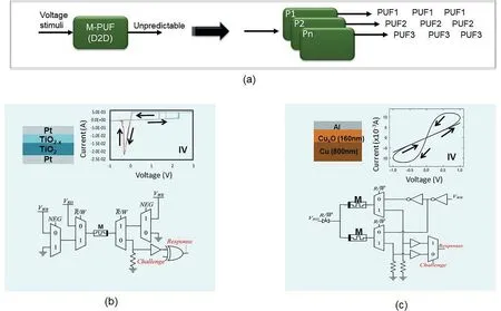
Fig.8.(a)Schematic demonstration of PUF functionality.(b)Experimental IV characteristics of Pt/TiO2–x/TiO2/Pt and circuit design of 1-bit M-PUF cell that utilizing the variations in memristor write times[102].(c)Experimental IV characteristics of Al/CuxO/Cu memristors and circuit design of 1-bit M-PUF cell that utilizing the stochasticfilament formation[103].The diagrams are adapted from the corresponding references.
2.3.Impact of memristive technology and further open questions/recommendations
M-PUF and M-TRNG security primitives for secret generation in hardware security applications benefit from the inherent property of memristive devices:their variability.It includes D2D,C2C and T2T variations.The D2D variation is due to the process variability,i.e.uncontrollable fabrication process fluctuations(for example thickness of structures or dopant concentrations),which manifest themselves in the physical nanoscale geometry.The C2C variation is due to the random distribution offilaments or charged ions/oxygen vacancies in the functional thinfilm,which are formed/ruptured or redistributed during memristive SET/RESET processes.The T2T variation refers to the current degradation during the continues read-out of the memristive states,i.e.the LRS/HRS reading current kept decreasing/increasing while applying continues reading voltage stimuli to the cell.In order to build reliable secure system for IoT,we need to consider the time-to-time(T2T)variation of memristive devices,which might compromise the statistical properties of constructed M-PUF or M-TRNG after a certain period of usage.
Further,the nonvolatility of emerging Mem-NV memory may change the established assumptions on their security and privacy properties.It can be problematic for security,as secrets are not destroyed automatically during power reset.It could also help the adversary to insert,hide and trigger Trojans.For example,a Trojan which transfers malicious code into a microprocessor's cache must do so only once if this cache is nonvolatile.Thus it is essential to consider possible resilience techniques for such security issues in the conceptualization and design phase of MPUF or M-TRNG.
It is also currently under-evaluated how memristive entropy sources for TRNGs and PUFs function under changing environmental conditions(e.g.,temperature gradients),stress(e.g.,excessive voltage)or aging.Security analysis,including the evaluation of secrecy and statistical properties for TRNGs,and uniqueness and reliability for PUFs,must take the mentioned parameter-dependency into account.Security properties must be guaranteed for devices working under different conditions,and at the same time,technology aspects such as yield and manufacturability must be considered.Developing effective security solutions at reasonable costs will require joint efforts from scientists from memristive technology,circuit design and manufacturing,and security.
A number of extensions to the basic PUF definition are known,and memristive devices can be helpful in their implementation.For example,the concept ofstrong PUFsorerasable PUFsmay be realized with emerging memristive devices.A recent suggestion for an attack-resistant strong PUF incorporates memristors and relies on their specific properties[105].Furthermore,a number of other emerging entropy primitives have recently been discussed in the literature.One example is theVirtual Proof of Realityconcept[106],where physical properties of a system,such as its temperature,geometry or proximity to a well-defined object,are verified remotely(over a communication link)based on PUF-inspired concepts.This is one novel class of entropy primitive involve advanced physical layer techniques that are able to provide entirely new security functions that have not been possible using traditional cryptographic techniques.In Ref.[107],the memristor-PUF is demonstrated to satisfy the requirement of VP of destruction,which is thefirst construction of VP of destruction based on electrical circuit.
3.From M-logic computing towards ciphers
Many security techniques are based on cryptography.In particular,it is not sufficient to generate and store a good secret key as explained above;it should also be processed in a manner that is resistant to attacks.Therefore,hardware circuits must be able to provide cryptographic functionality.
Ciphers are one major class of cryptographic primitives designed to provide confidentiality,i.e.,restrict access to information to authorized parties only.One can distinguish betweensymmetric ciphers,where parties share a common secret(secret key or encryption key)andasymmetric ciphers,where each party has a pair of a public and a private key.Asymmetric schemes avoid the need to securely distribute the secret key among parties,but they require longer keys and involve more complex(and therefore more power-consuming)mathematical operations than symmetric schemes.The security of all ciphers is based on the difficulty of solving certain mathematical problems,and therefore all known and new constructions undergo a scrutiny known ascryptanalysis,i.e.,attempting to circumvent the cryptographic protections;that a cipher is considered“secure”merely means that cryptanalytic efforts so far were unsuccessful.It is worth mentioning that the security of two most popular asymmetric schemes is based on the difficulty of problems that will be efficiently solvable by a sufficiently large-scale quantum computer once it will exist.Therefore,there is interest in alternative“postquantum”asymmetric schemes that have no known vulnerability against cryptanalysis performed on a quantum computer,but unfortunately are much more complex and expensive than the traditional schemes.
The focus of this section is on symmetric ciphers,but many ideas are applicable to asymmetric ciphers and to further cryptographic primitives,such as digital signatures,message authentication codes or cryptographic hash functions[108].Symmetric ciphers can be subdivided into two classes:streamandblock ciphers.Both types take as inputs a plaintextPand the keyk,and produce a ciphertextC=enc(P,k),whereencis the encryption function.The inverse function is calleddecfor decryption;if Alice has encryptedPand sent the resultingC=enc(P,k)to Bob who knows the keyk,Bob can obtain the original plaintext byP=dec(C,k),whereas an eavesdropper who interceptsCbut does not knowkcannot decrypt it.Stream ciphers processPbit by bit;once a bit ofPis supplied,the next bit ofCis produced(this can be realized by continuously generating a stream of key bits and XORing the plaintext bits with this stream;decryption works by XORing with the same generated key stream).Block ciphers take a plaintext message(called“block”)that consist of afixed number of bits and encrypt them at once;for example,the popular Advanced Encryption Standard(AES)supports blocks of size 128,192 and 256 bits.
3.1.CMOS implementations of ciphers
Ciphers are mathematically well-defined mappings that work either on bits or on larger(but still discrete)objects,typically elements of afinite Galoisfield.Most ciphers consist of several basic operations applied one after another;these operations can be written as Boolean functions and mapped to digital hardware submodules.The outputs of a submodule can either feed the next submodule directly,or a register(array of storage elements)can hold this value before handing it over to the next submodule.All known techniques to optimize digital hardware can be applied to ciphers:the basic operations can be synthesized enforcing area,delay or power constraints;they can be parallelized or pipelined to increase throughput;they can be decomposed into simpler operations to reduce their area footprint.
Fig.9 shows as an example the organization of a possible typical circuit implementation the above-mentioned AES block cipher's 128-bit version.It takes a 128-bit plaintextPas input and applies 10 largely identical rounds to obtain ciphertextC.The cipher maintains a 128-bit state organized as a 4×4 matrix of bytes(8-bit pieces of information or,equivalently,elements of GF(28)).The state is set toPin the beginning of the computation,andCis simply the state after all the operations have been applied.The following specific operations are included:
·Key addition:A bitwise XOR with theround key ki,wherek0is the secret key and the subsequentki's are derived from it by a process called“key expansion”.Key expansion does not ensure independence betweenki's;an attacker who manages to learn one round key can easily reconstruct all other round keys includingk0and thus break the cipher.
·SubByte:A mapping(often called S-Box)is applied to each of the cipher state's 16 bytes.An S-Box maps(substitutes)a byte to a different byte,so 16 S-Boxes must work in parallel.This is the only operation in AES that is not linear in GF(28);a cipher which consists only of linear operations would be easily breakable by solving a system of linear equations.
·ShiftRows:Here,some of the bytes in the cipher state exchange their position within the same row with no modification(the content of the byte is unaltered).This operation,together with MixColumns,forms the“diffusion layer”which makes sure that any individual bit of the plaintext is spread over many bits of the ciphertext,preventing certain types of cryptanalysis.
·MixColumn:Here,the four bytes of each column of the cipher state are“mixed”by multiplying them with a predefined 4×4 matrix over GF(28).This operation is omitted in the last round.
All mentioned operations are combinational(memory-free),and it is possible to implement all 10 rounds of AES as a combinational circuit(as indicated in Fig.9).A more popular realization option is to implement the combinational logic of one round,a round counter and a 128-bit register.Then,the cipher state after a round is written into the register and the next round takes this state as input,thus reusing the same logic;this is iterated ten times.
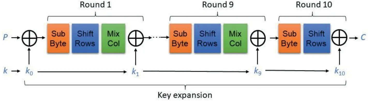
Fig.9.Organization of AES-128 block cipher.
While AES can be seen as a de-facto standard block cipher,a number of other block and stream ciphers are known,some of which are developed with an efficient hardware implementation as the prime objective(“lightweight cryptography”).The general principle described above for AES-128 can be transferred to other ciphers(and other cryptographic primitives).The operations are mapped to combinational(sometimes sequential)logic;the state is stored in registers;the plaintext is applied on the circuit's input and the ciphertext produced on its output.The secret key(which the combinational logic treats as a further input)is securely stored on the chip,either in protected non-volatile memory or generated by a TRNG or PUF.
3.2.Memristive implementations of cipher building blocks
Ciphers are digital circuits that consist of combinational logic and storage elements(registers).Combinational logic is composed of hierarchical submodules,which arefinally composed of logic gates.For instance,the AES block cipher includes S-Boxes and Galoisfield matrix multiplication as combinational sub-modules that can be mapped to logic gates,and registers to store intermediate results of the encryption.Hierarchy need not be purely combinational;for example,the Trivium stream cipher(not further discussed here)includes several sequential linear feedback shift registers(LFSRs)[109,110].In the following,we will discuss memristive logic,starting with implementing individual logic gates or small primitives,with multiplexer serving as an example,and continuing with memristive adders as examples of more complex combinational(sub-)modules.
3.2.1.M-XOR logic gate implementations
Fig.10 demonstrates the realization of Boolean logic function XOR by utilizing MRL,CRS-R and IMPLY logic families,which are introduced in Subsection 2.1.
By seamlessly integrating with the existing CMOS technology,a latency efficient hybrid gate is implemented by using MRL logic family based on TiOxmemristor with dual XOR/AND functionality[111].The presented hybrid gate structure is demonstrated in Fig.10(Column“M-XOR/MRL”),and consists of four memristors(M1,M2,M3,and M4),one transistor and one resistor.TE and BE represent top and bottom electrode of memristiors,respectively.Memristors M1 and M3 are TE-to-TE connected for logic OR or MAX operation,whereas M2 and M4 are BE-to-BE connected for logical AND or MINoperation.The XOR logic function can be realized by comparing the voltage levels between logic outputs OR and AND.The dual XOR/AND functionality is operated in a single clock cycle.In comparison to power consumption of XOR gate implementation based on CMOS technology with 10 transistors(61.11μW)[112],the MRL based XOR gate consumes much less power(14.38μW),and maintains reliable performance at high frequencies(up to 8 GHz).
CRS-R and IMPLY logic families are belonging to sequential logic concept,which has been introduced to realize the logic functions in a sequential operation with a set of clock cycles.M-XOR gate that implemented by CRS-R logic family requires a single memristor with complementary resistive switching behavior[11].The table in Fig.10(Column“M-XOR/CRS-R”)shows the realization of XOR with three clock cycles,including initialization(Ini.),writing(C.W)and reading(C.R)cycles.In CRS-R logic solution,the writing bias is determined by the potential of TE and BE,which depends on the logical variable A and B.In the initialization(ini.)/reading cycles(C.R),the logical input variables‘1’and‘0’identify the positive and negative writing/reading bias to the corresponding terminals,while the other terminal is grounded(GND).In writing cycles(C.W),the logical input variables‘1’or‘0’determine the positive or 0 V writing bias to the terminals.Note that,the reading bias in reading cycle C.R depends on the logic variable A,which leads to the correct logic output state of XOR gate.To accommodate stateful logics,a write-back step can be used to store such logic output state as corresponding resistance state in the same memristive device.M-XOR realized by IMPLY logic family requires four memristors and one resistor,where the logic input and output states are stored as resistance states in the operational memristors.The operational cycles are demonstrated in Fig.10(Column“M-XOR/IMPLY”)which are optimized based on the computational steps in Ref.[113].Thefinal output is saved as resistance state in memristor Y.
Many cryptographic functions are reversible(invertible;e.g.,every encryption function must be complemented by a decryption function to recover the plaintext by an authorized party who possesses the correct secret key).XOR gates are very often used in cryptographic blocks;for instance,the key addition in AES(Section 4.1)is simply an array of 128 XOR gates with inputs driven by the bits of the cipher state and the secret key coming from the key schedule.
3.2.2.Multiplexer exploiting memristive devices
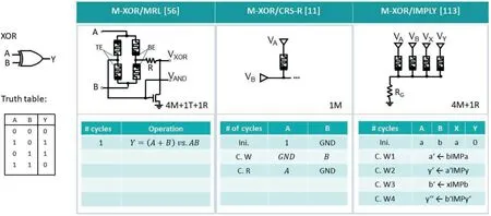
Fig.10.Implementation of memristive XOR logic gates by exploiting MRL[56],CRS-R[11],and IMPLY[113]logic families.The diagrams are adapted from the corresponding references.
Multiplexer(MUX)is one of the necessary logic units for implementing AES.Fig.11 compares and summarizes the circuit structures,operational device numbers and operational voltage cycles of the representative memristive 2-to-1 multiplexers based on MRL and IMPLY logic families[114].

Fig.11.Exemplary control sequences for 2-to-1 memristive multiplexers(M-MUX)by exploiting MRL and IMPLY[114]logic families.M-MUX based on MRL logic family is transformed based on the CMOS implementation,where further CMOS components for cascading gates might be needed.The diagrams are adapted from the corresponding references.

Fig.12.Comparison of representative N-bit memristive adder implementations based on IMPLY[[102,116,117]],MAGIC[118,119]and CRS[120]logic families.The circuit demonstrations for memristive adders are adapted from the corresponding references.The diagrams are all adapted from the corresponding references.
MRL-based M-MUX implementation(Fig.11,column“M-MUX/MRL”)is transformed from CMOS-based realization,which includes two memristive AND gates and one OR gate based on MRL logic families.Based on MRL logic family,no memristive NOT gate can be realized,and two transistors are applied to implement NOT gate.Not that,the cascading gates in MRL may require some signal amplification,e.g.,through insertion of CMOS buffers or inverters(not drawn here).By applying logic input variable to ports A and B,the 2-1 M-MUX function can be realized within 1 clock cycle.In comparison to MRL implementation,the 2-1 MUX function can be executed starting with one initialization logic cycle and further withfive sequential IMP logic steps with the help of IMPLY logic solution(Fig.11,column“M-MUX/IMPLY”).The logical input variables for MUX are stored in memristive devices S,A and B,and by exploitingfive memristive devices the logical output of MUX is computed and stored as memristance state in the memristive devices Y[114].
Multiplexers are essential building blocks of all circuits,including cryptographic functions.For example,the popular iterative(sequential)implementation of the AES-128 cipher from Fig.8 consists of four combinational blocks Key Addition,SubByte,ShiftRows and MixColumns that are used ten times(rounds).However,the last round of AES-128 differs from thefirst nine:MixColumn is skipped.To implement this,a 128-bit MUX can be inserted before key addition.This MUX receives the outputs of ShiftRows and MixColumns as inputs and is controlled by the round counter being compared with number 10:If the current round is 10,the multiplexer forwards the outcome of ShiftRows(thus skipping MixColumns),otherwise it forwards the regular MixColumn result.
3.2.3.N-bit memristive adder schemes
The representative N-bit memristive adder schemes based on IMPLY,MAGIC and CRS logic families are summarized in the table in Fig.12,where the structures of designed circuitry are compared in terms of operational device numbers and cycle numbers.
Based on IMPLY logic family,Lehtonen et al.[115]demonstrated logic circuit design ofN-bit full adder with 3N+5 memristors that connected in parallel.One additional resistor is needed with 88N+48 sequential operation cycles.Kvatinsky et al.[116]and Karimi et al.[117]proposed three improved logic architectures for IMPLY-basedN-bit full adder,i.e.serial structure [116],parallel structure [116] and parallel-series structure[117].With the optimized structure designs,the efficiency of implementation area or latency can be improved.
TheN-bit memristive adder schemes based on stateful MAGIC logic family are listed in Fig.12 with various design considerations by exploiting NOR and FALSE gates based on MAGIC concepts.In comparison to MAGIC based RCA memristive adder scheme[118],the area-and latency-optimized MAGIC-based adder schemes[119]needs further less area and latency.In general,the stateful MAGIC-based adder schemes demonstrate particular strong computation ability in dealing with more complex parallelism functions, which outperform the stateful IMPLY-based implementations both in area,speed and energy consumption.
Siemen et al.[120]presents two N-bit memristive adder schemes using CRS(complementary resistive switching)based sequential logic concept.For the CRS-based adder implementation,both carry and sum bits need to be computed sequentially(with the help of intermediate sum bit)with few operational cycles.In order to accelerate operation process,both the precalculation(PC)adder scheme and the toggle cell(TC)adder scheme are programmed to compute both the carry bit and intermediate sum bit simultaneously.The difference between two schemes is that:The PC adder scheme requires 2(N+1)+2 operational cycles with 2(N+1)devices in two word lines,thus the read-out of carry bit and the computation of sum bit can be programmed within one step in two word lines,whereas the TC adder scheme is operated in single one word line and more operational cycles would be needed(in total(4N+5)cycles and(N+2)devices).Thus the increased operational cycles are mainly due to the sequential read-out of carry bit and the computation of sum bit.Moreover,by using CRS memristive device with destructive reading,the read-out step must be written back to same cell in TC adder scheme,which consumes more operational cycles.Nevertheless,in general,the CRS-based non-stateful memristive adder schemes are showing potential of efficient implementation in terms of both area and latency than IMPLY and MAGIC-based approaches.
For example,the listed memristive implementations of 8-bit full adder in the table in Fig.12 based on IMPLY,MAGIC and CRS logic families require component numbers as less as 27 M+1R[115],5 M[119]and 10 M[120],which present great area saving potential in comparison to a single CMOS based 8-bit full with two eight-bit inputs and one eight-bit output which comprises of around 400T(400 transistors).Furthermore,the stateful memristive addition exploiting novel IMC architecture spares the energy to access the data from DRAMand to write the results back to cache,and costs energy for 32-bit in-memory addition within the range of 0.1–1 nJ(The exact energy cost is depending on the exploited specific version of MAGIC or IMPLY logic families)[119].While the estimated energy cost of conventional 32-bit addition by using von-Neumann architecture includes DRAM access energy of 3.2 nJ(50 pJ/bit[121]),32-bit adder operation energy of 0.1 pJ[122],and cache write-back energy of 30 pJ[123],which is much higher than the memristive IMC approaches.Thus the memristive IMC implementations are more suitable for IoT applications concerning the area and power consumption of addition operation in comparison to CMOS conventional approaches.
The additional criteria referring to the compatibility with the MCAs is also considered in the table in Fig.12.Only Kvatinsky's parallel approach and Karimi's parallel series approach require more complicated memristive crossbar architecture.In contrast,the introduced adder schemes based on MAGIC and CRS logic families are all compatible with common passive MCAs(as shown in Fig.6c)with less devices and a smaller number of cycles.The corresponding circuit design architectures for each adder scheme are illustrated at the bottom of Fig.12.
Inspired by the memristive adder implementations,the arithmetic in Galoisfield can be further realized for constructing memristive AES block cipher.Moreover,addition(and also multiplication,inversion and further arithmetic operations)in a Galoisfield can be realized by memristive logic as well,since memristive logic families are universal and can implement arbitrary functions.
3.3.Impact of memristive technology and further open questions/recommendations
Any implementation of security-relevant functionality must fulfill both general(security-unrelated)and security-related requirements.The implementation must obviously becorrect(e.g.,an AES-128 encryption circuit must indeed realize the AES-128 encryption)andefficientwith respect to some objectives,e.g.,area,power consumption or performance.This set of requirements generally applies to all circuits and not only security-relevant ones.Moreover,the implementation must besecure,i.e.,withstand certain types of attacks,such as side-channel analysis,fault-injections,or probing.The required extent of countermeasures against attacks depends on the considered types of attacks and assumed attacker capabilities.For instance,consider fault injection:one can assume a powerful attacker who can set any register within the circuit to a desired value,or an attacker who can decrease the power supply voltage of a circuit,resulting in poorly controlled and random failing patterns.Defending a circuit against these two types of attackers will demand different countermeasures with different costs[124].
This discussion applies to cryptographic circuits(e.g.,the AES block cipher)constructed from emerging memristive devices.As has been indicated above,a basic decision for all memristive circuits is the choice of the memristive logic family.Recall Fig.10,where an M-XOR needs more chip area but less sequential cycles when the MRL logic family is used compared to the IMPLY logic family,whereas the CRS-R-based MXOR can be seen as a compromise between the two.It can be an important factor that some of the logic families in question(with proper circuit topology)can be realized by standard MCAs.
Another parameter that does not occur in conventional CMOS design is the ease of integration of the memristive logic with CMOS.Most logic families require CMOS peripheral circuits for synthesizing and auxiliary control signals,and the MRL logic family is inherently hybrid because its set of memristive primitives is not universal:it lacks inversion.
Furthermore,the AES block ciphers can offer a high security level,but for the IoT applications which require further small area and low-power dissipation,lightweight encryption algorithms with reduced complexity,such as KATAN[125],can be a more attractive option.For emerging cryptographic solutions with a higher complexity(e.g.,postquantum asymmetric algorithms),the memristive devices combine the integration density and access times of today's SRAMs with the non-volatility of flash memories;they enable novel cache hierarchies well-suitable for power-sensitive applications[126].An attractive inherent feature of memristors is the ease of implementation of stateful algorithms[54],which can be employed for a straightforward implementation of“nonces”(number used once)often needed by advanced cryptographic schemes.An interesting property of memristive devices to support storage and manipulation of multi-level data(thus allowing multi-valued computations in a natural way)is largely unexplored in the context of modern cryptographic schemes.
4.From Mem-AI computing towards security feasibility:attacks and protections
Machine learning(ML)is changing the world in security.ML-based defenses can be used to improve system security,whereas ML-based attacks may also cause major security issues in hardware systems.As Mem-AI computing paradigm provides great potential to be the leading solution for ML implementations in IMC for IoT,it is essential to explore the security implications of Mem-AI computing on ML-supported defenses and attacks on hardware system,which is insufficiently investigated yet.
4.1.Machine-learning oriented security assessment
Machine learning(ML)can play a major role in both:attacks and countermeasures on secure hardware.In the attack context,ML can improve the efficiency of side-channel analysis[127]or compromise the security of PUFs via“model-building”attacks[128].When speaking about defenses,ML can help identify anomalous system behavior that may point to an(attempted or successful)attack.ML is a computationally intensive task,and it can be advantageous to provide dedicated hardware that supports ML operations.On the adversarial side,such dedicated ML hardware is useful but not strictly required,because attacks are usually mounted by adversaries with powerful compute servers.On the defense side,in contrast,ML-based anomaly-detection solutions must be implemented directly on-chip and monitor the system behavior in real time.
4.2.Implementations of memristive artifi cial synapses
Inspired by the biological understanding of synaptic and neuronal behaviors(Fig.13a),the models for artificial synapses and neurons are proposed as the building blocks for implementing ML applications in both training and testing processes.As introduced in Section 2,the emerging MCAs can provide a promising hardware realization of artificial neuron networks,and both artificial synapses and artificial neurons(Fig.13b)can be implemented by emerging memristive and hybrid CMOS-memristive devices,respectively.

Fig.13.Memristive implementations of ML building blocks.(a)Schematic demonstration of biological and memristive arti f icial neurons and synapses.(b)Illustration of functional connection for arti f icial neurons and synapses by using MCA.(c)Con f igurations of memristive arti f icial synapses,including 1M-synapse[129,130],1T1M-synapse[130],and 2M-synapse[132,133](d)Realizations of arti f icial neurons,including I&F neuron circuit[138]and summing/thresholding neuron models for 1M-synapse[140–142]and 2M-synapse[143].The variable i represents the number of corresponding word line,while j represents the number of corresponding bit line.The copy right permission is available for I&F neuron in Ref.[138],and the other diagrams are adapted from the corresponding references.
Fig.13c demonstrates different configurations of memristive artificial synapses.The artificial synapse can be realized by using one single memristor(1M-synapse)[129,130],which is efficient in terms of on-chip area and power consumption.But such configuration suffers from common sneak path problems of MCAs.One possible solution would be to add one transistor in series of memristor(1T1M-synapse)[131],which solves sneak path issues but requires more energy than 1M-synapse.Another popular configuration for artificial synapse is based on 2 memristors(2M-synapse)[132,133],which doubles the implementation area size but allows implementing negative synaptic weights that needed in the neural networks.The voltage stimuli generated from artificial neurons in different word lines are applied over the MCA based memristive synaptic network,and the generated current Iijcan be sensed from each bit line.The energy consumption per synaptic event is critical for the performance evaluation of AI system.For memristive artificial synapses,it is easy to reach several pJ per synaptic event[134,135],or even several hundresds of fJ[27,136],which is close to the biological brain,whereas the most reported CMOS based artificial synapses usually operate at~nJ per event level[137].Considering the Mem-AI system with 105synapses[138],the energy cost of synaptic operations can already significantly be reduced by orders of magnitudes in comparison to conventional CMOS technology.
Furthermore,the neuron cell sums up the input signal stimuli from all artificial neurons in different word lines and generates voltage spikes transmitted to other neurons(not shown)through memristive artificial synapses(Fig.13b).According to such equivalent representation of biological neuron,thefirst proposed neuron model is Integrate and Fire(I&F)neuron model[139],which contains the major functions as current integration and spike generation(Fig.13d).However,for the energy constrained IoT applications,such artificial neuron models are not practical and applicable due to the large on-chip area and high power consumption.The threshold-logic-based linear neuron model,which is based on summing amplifiers and comparators,is usually utilized for ML implementations.The conventional summing and thresholding neuron configuration[140,141]is demonstrated on the right side of Fig.13d,where the summing amplifier accumulates the input current and sources the corresponding voltage signal to the comparator.The comparator generates the voltage spike to the next layer of neurons if the amplifier output voltage is above the threshold.An alternative approach for artificial neuron is based on hybrid CMOS-Memristor design[142].Thefirst amplifier with memristor Mfis both to scale the output voltage and implement the sigmoid activation function,where the reconfigurable resistance of memristor Mfis utilized to control the feedback gain,and the second amplifier is for inverting the output.For the 2M-synapse,the artificial neuron is combining the voltage outputs from both positive and negative artificial synapses by using two sets of summing amplifier and comparator circuit[143].The proposed artificial synapses and neurons are utilized for different ML architectures,for examples the traditional artificial neural network(ANN)[131,144]and the convolutional neural network(CNN)[145].
For further IoT application,efforts have also been made to utilize single power constrained memristive device for highly efficient edge computing,i.e.to associate memristive device with sensors for data processing purposes.As an example,in an artificial haptic perception system,a single Nafion-based organic memristive device is integrated with a piezoresistive pressure sensor in order to mimic the functionality of an artificial synapse for application in human perception[146].The basic synapse functions including paired pulse facilitation/depression and spike timing dependent plasticity behaviors are mimicked in one Nafion-based memristor.Furthermore,the memristive devices can also be used as memory device for edge computing.Most recently,an artificial spiking afferent nerve[147]is reported based on a single Mott memristive device,which is applied as an interface for converting the analog sensory signal into spikes for further data processing.
4.3.Impact of memristive technology and further open questions/recommendations
The impact of Mem-AI computing on security assessment can be explored from two aspects:one aspect is to conduct the most effective use of advantages in Mem-AI implementations for conventional CMOS oriented ML-supported attacks and defenses,i.e.side channel analysis or strong PUF modelling,anomaly detection during system operation.The other aspect is to understand the security feasibility on Mem-AI computing design itself.
The energy consumption of Mem-AI computing system is highly depending on the various memristive networks further in association with different learning strategies,which can be estimated both in element device level and network learning level[148].In general,the MCA-based Mem-AI computing with highly parallel architectures provides attractive features to implement different types of ML algorithms,which can significantly reduce the power and area consumption by orders of magnitudes in comparison to conventional CMOS technology.Therefore,it is also predictable that the ML-supported attacks and defenses can be more efficiently implemented by memristive technology instead of standard CMOS technology.Thus Mem-AI computing system offers promising improved options for hardware-oriented ML oriented security application in big data and data-intensive applications in IoT.
Furthermore,the impact of memristive technology on ML realizations can also be explored by studying the vulnerability and resilience in Mem-AI computing system itself.For example,it has been demonstrated that Mem-AI computing system can prevent an attacker with physical access from the replication attack of proprietary learning model[149].The learning model is the key for the ML implementation system.If the attacker has physical access to the device,the learning models which are exploited in Mem-AI computing system are exposed to the risk of being attacked by the attacker in the way of observing the inputs and outputs variables of the system.As has been shown in Ref.[149],time-to-time(T2T)variability(as the third intrinsic variation of memristive devices beyond D2D and C2C variations)can be used for preventing replication attacks against secure Mem-AI computing systems.
Mem-AI computing systems might cause further security issues.For example,as one major technical issues for the Mem-AI computing implementations,i.e.the nonlinear G-response of memristive cells[150]can decisively affect the performance of artificial neural network(e.g.strong degradation of neural network accuracy during online learning).Thus the researchers are struggled to realize the preferable linear conductance response(G-response)of artificial synaptic cell recorded under application of identical excitation pulses for training process during ML implementation.There are several solutions proposed to fulfill this purpose,for instance to apply non-identical voltage pulses with varying pulse widths for achieving the linear G-response.However,one needs to take care to not compromise security by creating information leakage via non-identical voltage stimuli.
Furthermore,Mem-AI computing system enables edge computing[151]for IoT.Edge computing,where large volumes of data are processed on edge devices,is considered as a natural complement to conventional cloud-centered computing.Mem-AI computing system with its scalability,small on-chip area,low energy dissipation and adaptability is suitable to be integrated directly into the edge devices,for example thefirst programmable memristor computer as demonstrated in Ref.[152],which can process the data by using Mem-AI computing system on edge devices,such as smartphones and sensors.It significantly reduces the long-distance communication between sensor array(edge)and cloud data center,and enable better security and privacy by avoiding transmission through unprotected media.
5.Security threats to memristive primitives
The material above focuses on expected advantages of memristive technologies for security applications.It is,however,a legitimate question whether memristive primitives themselves can give rise to new kinds of security attacks.After all,their physical properties are different from the conventional CMOS electronics,and at least in theory,new attack vectors might exist,or known countermeasures that work well for CMOS might be less effective.
Physical attacks are known in principle for all functions discussed above:entropy primitives;ciphers;and ML components.One can distinguish between passiveside-channel analysis,where an attacker observes,e.g.,the power consumed during encryption to deduct secret information[153]and activefault-injection attackswhere an adversary induces physical disturbances during encryption[124].A number of countermeasures are known against physical attacks,and a secure system should incorporate some of them.
Physical attacks against memristive implementations,and consequently protections against such attacks,are not yet sufficiently understood.One should pay special attention to potential attack mechanisms that are unique for memristors and do not exist in conventional CMOS.A memristor can recall the last resistance state stored in the device even after the power has been turned off.An attacker might try to utilize such memory effects during side-channel analysis to leak information from previous logical operations.When discussing information leakage through the power side-channel,it is important that the input voltages in both MRL and CRS-R logic families depend on their logic values,which can create new sources of information leakage.Moreover,sequential voltage operation required by some memristive logic families plays a crucial role in designing functional security circuits,assessing their vulnerability to physical attacks,and developing suitable countermeasures.They give rise to trade-offs between different design parameters:area,latency,power consumption,and vulnerability to(or difficulty of protection against)physical attacks.Moreover,peripheral CMOS logic added to support memristive operation must be considered when evaluating the side-channel information leakage.
A further dimension is spanned by(active)physical attacks,e.g.,an adversary advertently applying laser or electromagnetic pulses to the entropy primitive with the intent to either disrupt its operation or to make the generated secret predictable.
An emerging target of physical attacks is the AI hardware,and there the intellectual property associated with the implemented neural network itself.In contrast to a cryptographic circuit such as the AES block cipher,where the functionality is known and only the secret key is confidential,an AI circuit implements a function that has been obtained by a laborious and expensive process:constructing or selecting an architecture,putting together the training set,and obtain the individual weights by processing-intensive training.Physical attacks can be mounted by adversary to deduce the architecture(number and shape of layers)and the weights associated with the individual synapses from measurements of,for example,electromagnetic emanations of the circuit[154].A number of protective approaches are under development,e.g.,watermarking[155]where a signature of the legitimate owner is embedded into the NN(and therefore its circuit implementation)orfingerprinting[156]where the signature includes a unique identifier orfingerprint to distinguish between different users of the NN.When memristive logic is used for AI circuits,their vulnerability to this type of reverse engineering threats must be assessed.
The resistance of memristive systems to physical attacks is still rather unexplored.Among the few results published so far are works on counteracting power analysis[157]and active fault-injection attacks against resistive memories[158].In Ref.[159],a special memristor-based neural-network implementation of the AES S-Box is investigated for power analysis resistance.A deep understanding of attack vulnerabilities of broader classes of secure hardware discussed in this article is still lacking,even though it is a necessary prerequisite to design effective countermeasures against physical attacks.
6.Concluding remarks
IoT demands dedicated low-cost smart chips,including low-cost on both power and area consumption.The emerging low-power memristive technology with their intrinsic nonvolatile and reconfigurable properties and potential numerous advantages,i.e.high chip density,high power efficiency,high uniformity,fast switching speed etc.,enables Mem-Logic computing and Mem-AI computing and reduces the data transfer by incorporating processing capabilities into the Mem-NV memory itself,laying promising foundation for enabling IMC paradigms with highly parallel processing capability.The memristive IMC paradigms,including Mem-Logic computing and Mem-AI computing,enable novel non-von Neumann architecture,which significantly reduce the energy consumption and miniaturize the chip size by orders of magnitudes in comparison to conventional CMOS technology.This review article surveys the power and area efficient secure implementations based on emerging memristive designs for IoT.One main focus of this review article is the emerging nanoelectronic memristive technology,and its impact on security.We take the three major application approaches of memristive technology as the starting point,i.e.Mem-NV memory,Mem-Logic computing and Mem-AI computing,and further explore the higher-level applicationoriented impact of memristive technology on three corresponding cryptography areas,i.e.secret key generation,crypto functions and MLrelated attacks/defenses.It has been demonstrated that the security implication of memristive secure hardware systems is easier accessible if we study the security vulnerability and resilience of their corresponding memristive application.This review article brings together the views of researchers from material science and hardware-oriented security,and bridges the gap between memristive applications-level features and their further usage in hardware security systems.This invited review article can serve as a guide for the future implementation of memristor-oriented reliable and secure systems with constrained energy and area cost in IoT applications.
Declaration of competing interest
The authors have no con flict of interest to declare.
Acknowledgements
This invited review article is supported by the DFG(German Research Foundation)Priority Program Nano Security,Project MemCrypto(Projektnummer 439827659/funding id DU 1896/2–1,PO 1220/15–1).N.D.and H.S.acknowledges the funding by the Fraunhofer Internal Programs under Grant No.Attract 600768.We are thankful to two anonymous reviewers for their constructive feedback.
杂志排行
Namo Materials Science的其它文章
- GUIDE FOR AUTHORS
- Editorial for a special issue“Nano energy materials and devices for miniaturized electronics and smart systems”
- Aim & Scope
- A comprehensive review of miniatured wind energy harvesters
- Recent developments of stamped planar micro-supercapacitors:Materials,fabrication and perspectives
- Advanced architecture designs towards high-performance 3D microbatteries