Recent developments of stamped planar micro-supercapacitors:Materials,fabrication and perspectives
2021-07-28FeiLiYangLiJiangQuJinhuiWangVineethKumarBandariFengZhuOliverSchmidt
Fei Li ,Yang Li ,Jiang Qu ,Jinhui Wang ,Vineeth Kumar Bandari ,*,Feng Zhu ,Oliver G.Schmidt ,e
a Material Systems for Nanoelectronics,Chemnitz University of Technology,09107,Chemnitz,Germany
b State Key Laboratory of Polymer Physics and Chemistry,Changchun Institute of Applied Chemistry,Chinese Academy of Sciences,130022,Changchun,China
c Center for Materials,Architectures and Integration of Nanomembranes(MAIN),Chemnitz University of Technology,09126,Chemnitz,Germany
d Institute for Integrative Nanosciences,Leibniz IFW Dresden,01069,Dresden,Germany
e School of Science,Dresden University of Technology,01062,Dresden,Germany
Keywords:Microsupercapacitors Stamping Microfabrication Miniaturized electronics Energy storage devices
ABSTRACT The rapid development of wearable and portable electronics has dramatically increased the application for miniaturized energy storage components.Stamping micro-supercapacitors(MSCs)with planar interdigital configurations are considered as a promising candidate to meet the requirements.In this review,recent progress of the different stamping materials and various stamping technologies arefirst discussed.The merits of each material,manufacturing process of each stamping method and the properties of stamping MSCs are scrutinized,respectively.Further insights on technical difficulties and scientific challenges arefinally demonstrated,including the limited thickness of printed electrodes,poor overlay accuracy and printing resolution.
1.Introduction
Miniaturized flexible,wearable and portable electronics are imminently demanding thin and lightweight energy storage devices(ESDs)with long cycling stability,low manufacturing costs and good areal/volume energy[1–6].Unfortunately,as the primary choice of ESDs,conventional microbatteries(MBs)with sandwich structures often sustain heavy weight,bulky volume,short lifetime as well as low power density[7–13].These factors continually plague their application in wearable and implantable microdevices.Therefore,it is essential to fabricate a new generation of on-chip miniaturized energy storage devices(MESDs)avoiding these shortcomings to replace or supplement MBs[14–16].
Compared to traditional batteries and capacitors,electrochemical capacitors,also called supercapacitors(SCs),were extensively investigated in recent years because of their outstanding performance of quick charge-discharge,ultra-long cycling life and low maintenance cost[17–25].Through different energy storage and conversion mechanisms,SCs are classified into electrical double-layer capacitors(EDLCs)and pseudocapacitors.EDLC capacitance comes from the absorption and adsorption process of cations and anions near the electrolyte/electrode interface;therefore it highly relies on the specific surface area of the EDLC-type materials.During the charging process,anions move towards the positive electrode and cations move to the negative electrode,with electrons transferring from negative to positive electrode through the external loop.In the discharging process,the moving direction of ions and electrons would be reversed.Different from EDLCs,pseudocapacitors store energy through a faradaic process that contains fast and reversible redox reactions occurring at or near the electrode surface.When a potential is applied,the electrode materials undergo reversible redox reactions,generating charges and resulting in faradaic current passing through the SC cell[26–31].Since the two types of electrode materials have different physical and chemical properties,their differences will also be re flected in the different performance of electrochemical tests.The EDLC material has better rate performance and cycle stability because of its better conductivity and larger specific surface area.However,the charge redistribution caused by the movement or loss of charged ions adsorbed on the electrode due to concentration gradient will lead to self-discharge.Pseudocapacitance materials have a large capacitance due to the Faraday reaction;but the poor electrical conductivity limits their wide application.From the perspective of structural configuration,the typical conventional SCs are vertical sandwich structures consisting of a separator,two electrodes,and afilled electrolyte.The characteristics of the sandwich structure increase the difficult of device miniaturization,which cannot fulfill the requirements of continuous miniaturization of micro electro-mechanical systems(MEMS)[32–40].Accordingly,much research is conducted on microsupercapacitors(MSCs)in recent decades.Different from traditional sandwich-type SCs,MSCs often rely on in-plane configuration with interdigital micro-electrodefingers.Electrolyte ions transport rapidly and expediently between the narrow interspaces of the interdigitalfingers,providing fast charge-discharge rates and high power densities.These planar interdigital configurations possess obviously merits over the sandwich-structured MSCs[41–45].(MSCs with stack structures andfiber-shaped structures are not mentioned in this review,because these two structures have been well-reviewed in some recent literature[46–52].)For example,the narrow space between electronically isolated micro-electrodes in MSCs with in-plane interdigital configuration can efficiently avoids the need of a separator because,which is important integrant in traditional sandwich-type MSCs.Micro/nano-technology can precisely control the distance between the interdigitalfingers,thereby further reducing the ion transport resistance,which contribute to increase power density and improve the frequency response features[53–55].
Meanwhile,the adjustable design of the interdigital electrodes of the MSCs makes their performance indicators customizable.For instance,the energy density and area-specific capacitance within a given footprint area can be efficiently developed by increase the thickness of electrode materialfilms.At the meantime,the power density and ion diffusion length are only slightly compromised due to the primary ionic transport in the lateral direction of the MSC[56–58].Finally,the planar interdigital configuration can accelerate the integration with various portable on-chip electronic components on different substrates,which contributes to the miniaturization of the entire device[59–61].However,even with these merits,challenges such as complex patterning technologies still limit the commercial use of MSCs in portable electronics and on-chip microsystems withinfixed and small footprint area.
To date,traditional techniques employed in the interdigitated MSCs commonly divided into two categories.Thefirst strategy often contains complicated photo-lithography procedures(For example,spin-coating,soft/hard baking,ultraviolet exposure and development),O2plasma etching,and metal collectors evaporation.Moreover,the connection lines between the current collectors can result in a reduction of specific gravimetric and volumetric capacitances and sacrifice the flexibility of MSC device.Therefore,integrating lithography and related processes into process flows specifically for wearable and flexible electronics is difficult and high cost[62–64].
In order to avoid and solve these problems,the second strategy of developing interdigital electronic devices was formed and developed.In the past decades,printed electronics has received extensive attention thanks to the gradual development of the nano-materials and increasing maturity of micro/nano-technology [65–68].Compared to the micro-fabrication base on lithography and related techniques discussed previously,the printing electronic fabrication strategy is more environmentally friendly because it generates little material waste and pollution and requires lower energy consumption[69,70].Besides,a variety of stretchable and flexible substrates can be employed in printed electronics,instead of depending solely on traditional rigid substrates[71,72].With these two outstanding features,printing techniques provide the possibility for green and high-throughput fabrication of integrated,low-cost,portable and wearable electronics.
Generally,printing technologies comprise two categories,printing not utilizing templates,and printing requiring templates.For the former,the primary printing techniques without templates are 3D printing and inkjet printing[73,74].Regarding the latter,printing procedures requiring templates include screen printing,spray printing and stamping[70,75,76].Among them,stamping technique is straightforward,scalable and low-cost for flexible MSC devices.Therefore,the recent advances of stamping MSCs on flexible substrates were discussed in detail,including ink materials,stamping methods and properties of stamped MSC devices,as shown in Fig.1.

Fig.1.Schematic illustrations of the stamping ink materials,stamping method and properties of stamping planar MSCs.Reproduced with permission.Reproduced with permission[76,101,109,128,130].
2.Materials for stamped MSC
The preparation of printing ink is the essential part of stamping.Highperformance stamping inks of the printable MSCs require:i)high electrical conductivity for rapid electron charge transfer;ii)outstanding electro-performance for satisfactory areal capacitance,high energy,and long-life cycle;iii)excellent mechanical compliance and strength to adapt to deformation;iv)appropriate physical performance(e.g.,rheology,viscosity,drying rate,and surface tension)for high printing reliability and resolution;and v)high adhesion with the appointed substrate[77–85].To satisfy the demands mentioned above simultaneously,printable electrode ink systems typically contains three components:active materials,inert organic additives/binder,and suitable solvents.The performance of stamping MSCs is directly related to the conductivity and electro-properties of the electrode materials,the dispersibility of active micro/nano-particles in the solvent,and the uniformity of printing products.Here,the commonly used stamping materials for flexible MSCs are discussed.
2.1.Graphene-based stamping ink
Graphene has been under numerous investigations for its remarkable performance including ultra-high specific surface area of 2630 m2g-1,excellent electrochemical properties,and high flexibility[86–89].Because of these outstanding properties,graphene fulfill the requirement of various purposes in ESD applications.Similar to the various carbon-based materials such as active carbon(AC)[90],carbon nanotubes(CNTs)[91],onionlike carbon(OLC)[92],and carbide-derived carbon[93],high-performance graphene-based MSC stores energy by quick ion adsorption and desorption,and forms electrical double layer(EDL)of electrons and electrolyte ions at the interface of electrode and electrolyte(EDLC mechanism)[94–96].Additionally,the ultra-thin thickness,large surface area,and mechanical robustness and flexibility of two-dimensional(2D)materials bring satisfactory advantages in interdigital-structure MSCs,in which high rate performance,superior cycling stability and ultrahigh power density can be easily achieved by utilizing the lateral ions transport between the adjacent 2D layers[97–100].In addition,their flexibility and nontoxic and nonhazardous features could fulfill stringent requirements of wearable and portable electronic devices.Accordingly,some works in literature demonstrate the stamping manufacturing process with high conductivity graphene ink.
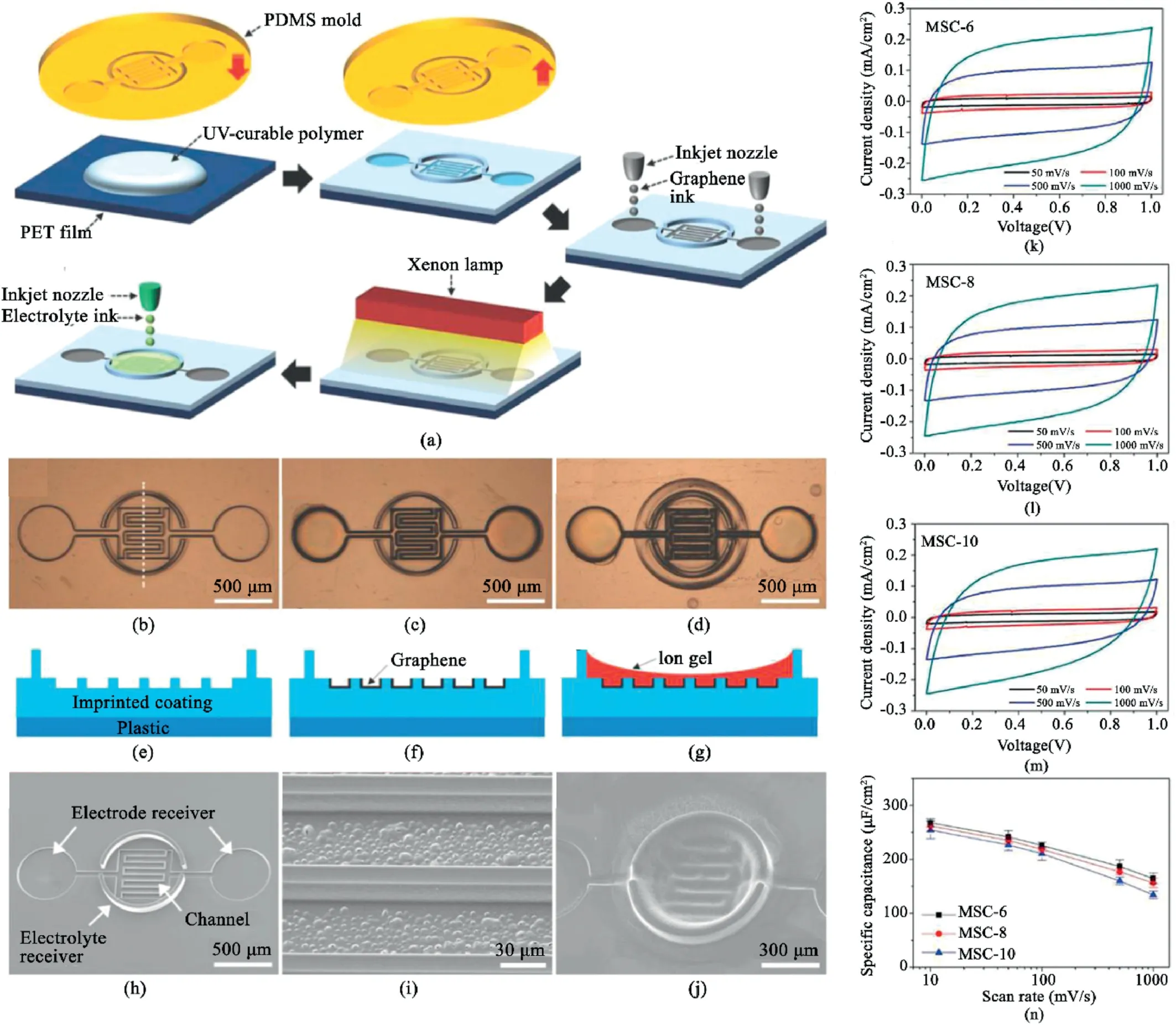
Fig.2.(a)Printing illustration for MSC devices utilizing the self-aligned capillarity-assisted lithography process.Optical photographs and the corresponding crosssectional illustrations of the MSCs after(b,e)stamping the UV-curable polymer,(c,f)inkjet printing the electronic ink in the capillary channels,and(d,g)patterning the ion gel ink.SEMimages of(h)the stamped receivers and channels,(i)graphene ink in channels,and(j)complete MSC device.(k–m)Cyclic voltammetry profiles of different MSC devices at various scan rates from 50 to 1000 mV s-1.(n)The specific capacitance of the devices as a function of the scan rate for the CV characterization.Reproduced with permission[101].
For example,Hyun et al.report a self-aligned scalable and efficient printing manufacturing of graphene-based planar MSCs on polyethylene terephthalate(PET)film using the capillarity of graphene inks in the asprepared micro-channels[101].Fig.2a depicts the schematic diagram of the stamping and printing process of the interdigital MSCs.Firstly,polydimethylsiloxane(PDMS)stamps and ultraviolet(UV)-curable polymer were employed to imprint receivers and capillary channels on PETfilms.Regarding the fabrication of PDMS stamps,photolithography technique was utilized to pattern the required capillary channels on a Si-based master mold.Then,the channels were formed by pressing the photopolymer on a plasma-treated PETfilm by the as-prepared PDMS stamps.Subsequently,the PDMS stamps were separated after UV curing of the polymer,thus the electrode channels and receivers can be obtained on the photopolymer coating.After microstructures are stamped on flexible PET substrate,electronic inks are inkjet printed in the micro-receivers and transported to the coterminous channels by capillarity,ensuring the ingenious patterning of graphene inks in complex channels.The optical microscope photographs and the corresponding cross section view of the in-plane flexible MSCs on PET plasticfilms are shown in Fig.2b–j.This facile printing process provides precise operation metrics and outstanding electrochemical performance with small footprint(<1 mm2of the interdigital area),high lateral spatial resolution(minimum size of 20 μm),remarkable area-specific capacitance(268μF cm-2),and excellent reliability(44 samples with 100%yield)(Fig.2k–n).
2.2.MXene-based printable ink
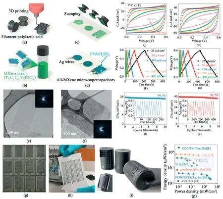
Fig.3.(a–d)Illustration of stamping process of MXene-based MSCs.(e–f)TEM images of d-Ti3C2T x and Ti3CNT x layers.Inset shows the selected area electron diffraction(SAED)pattern.(g)As-stamped devices with 12 interdigitated structures.(h)The as-prepared I–Ti3C2T x by rolling stamping.(i)The 3D-printed cylindrical stamps.(j)CV curves,(k)GCD profiles,and(f)Cycling stability of Y–Ti3C2T x.Inset displays several the GCD cycles.(m)CV curves,(n)GCD profiles,and(o)long-cycle property of I–Ti3C2T x.(p)Ragone plot comparison.Reproduced with permission[109].
In the last decade,new categories of novel 2D transition metal nitrides or carbides draw worldwide attention[102–104].Among them,MXene has shown remarkable potential in the application for high-performance ESDs electrode material.MXene material is came from layered hexagonal nitrides and carbides,also called MAX phases,in which A represent an A-group element(e.g.Ga and Al).Typical MXene material can be synthesized by facile etching the A-group elements from layered hexagonal nitrides and carbides.Additionally,MXene is generally marked as Mn+1XnTx,where Mis a transition metal(Ti,Nb,Mo),Xis nitrogen or carbon(n=1,2,or 3),and Txrepresent a functional group(=O,–F,and/or–OH).To date,more than 20 types of MXenes have been synthesized.Among them,Ti3C2Txdisplays significant promise because of its remarkable conductivity(~6500 S cm-1),surface hydrophilicity,and ability of facilitating ion intercalation.Regarding the metallic conductivity,Ti3C2Txdisplays higher value than solution-synthesized graphene-based materials,permitting the Ti3C2Txelectrodes to act as both current collectors and MSC active materials.Secondly,viscous and stable colloidal suspension can be obtained due to the hydrophilic groups delaminated from the MXene surfaces;the Ti3C2Txink can be straightly utilized without the polymer or surfactant additives.Lastly,its ability to conduct intercalation with electrolyte ions in adjacent MXene layers facilitates the cation adsorption,allowing charges to be stored into swollen MXene channels,accompanied by fast expansion and contraction of the MXene layers.Therefore,Ti3C2Txelectrode can offer both high capacitance and energy at targeted rates.These advantages of MXene and the facile,scalable,and environmentally friendly preparation process make stamping MXene-based MSCs the most potential candidate for flexible electronic devices[105–108].
Zhang et al.reported a facile and rapid stamping fabrication for Ti3C2Tx-based MSCs with high areal capacitance and good flexibility[109].The illustration of the stamping procedure of MXene-based devices is described in Fig.3a–d.Firstly,3D-printed method was employed to fabricate well-designed stamp shapes(Fig.3a).Various stamp design(e.g.interdigital/Yin and Yang/spiral)and thefinger structure parameter(e.g.width/numbers/gaps)can be designed quickly and efficiently through computer-aided control.Subsequently,the Ti3C2Txor Ti3CNTxinks(Fig.3b)brushed on the hydrophilic and rough stamps surface were pressed tightly on a desired substrate(e.g.office paper or PETfilm)(Fig.3c).After coating the PVA/H2SO4electrolyte,attaching Ag wires,and vacuum-drying overnight(Fig.3d),the all-solid-state MXene MSC devices can be achieved(Fig.3g–i).The stamped flexible Ti3C2Tx-based MSCs demonstrate good electrical properties with high area-specific capacitance(61 mF cm-2at 25μA cm-2),long cycling life(93.7%after 10000 cycles),and high energy density(0.76μWh cm-2).However,the Ti3C2TxMSCs display a low operating potential of 0.6 V as MXene is tend to be oxidized at high anodic potentials(Fig.3j–p).
The same group demonstrated one-step manufacturing of Ti3C2MXene-in-water inks without additive for MSC devices[110].The aqueous Ti3C2MXene inks are suitable for printing,writing,and stamping on various substrates.Different from typical particle inks which need subsequent annealing test to improve the conductivity,the aqueous Ti3C2MXene inks can achieve remarkable conductivity directly drying in air at room temperature(RT).Notably,high-performance MSCs without metal current collector can be rapidly prepared utilized with the conductive Ti3C2inks on flat or curved substrates.
2.3.Pseudocapacitive material-based printable ink
Pseudocapacitive materials for MSCs can be divided in two categories:transition metal oxides(e.g.,RuO2[111],Co3O4[112],NiO[113],MnO2[114],and V2O5[115])and conductive polymers(e.g.,PANI[116],polypyrrole(PPy)[117],and polythiophene[118]).Pseudocapacitive materials often possess higher capacitance and energy than those carbon-based EDLC electrode materials owe to their invertible electrochemical redox reactions during the charge-discharge process[119,120].However,pseudocapacitive materials generally suffer from poor electrical conductivity and have low specific surface area,result in low rate capability,solubility,and limited cycle lifetime.These negative characteristics limit the specific capacitance of pseudocapacitive materials to a level far from the theoretical value,especially at high rates,thus hindering their wide application[121,122].Accordingly,improving specific surface area,raising the electrical conductivity by introducing conductive polymer become an effective strategy for pseudocapacitive material used in stamping ink systems.
In Jia's work,3D PANI nanotube gel was synthesized by utilizing tetraphenyl porphyrin tetrasulfonic acid interlayer(TPPS)as crosslinking agent and dopant.Subsequently,MnO2nanosheets uniformly growth on the PANI nanotube surface,forming coaxial MnO2/polyaniline binary composite[123].Stamping of MnO2/PANI MSCs is described in Fig.4a–d.The interdigitated stamp shape was 3D-printed by computer control atfirst(Fig.4a).The MnO2/PANI ink was subsequent coated on the rough surface of the 3D-printed stamp.The flexible MSCs can be assembled byfirmly pressing the ink onto desired substrates(Fig.4c).The assembled asymmetric MSC displays high areal capacitance 22.5 mF cm-2at a scan rate of 10 mVs-1(Fig.4j–i).

Fig.4.(a–d)Stamping steps of interdigital MSCs.(e)SEM image of T-PANI.(f)TEM image of MnO2/T-PANI.(g)CV profiles of PC and MnO2/T-PANI.(h,i)CV and GCD profiles of MnO2/T-PANI//PC at various potential voltages.(j,k)CV and GCD profiles of MnO2/T-PANI//PC under 1.8 V.(l)Cycling performance of MnO2/TPANI//PC.Reproduced with permission[123].
3.Stamping fabrication techniques
As a template-based printing process,the reported stamping is mainly classified into four overarching categories:gravure printing,letterpress printing,flash foam–assisted stamp printing and stamp-assisted printing.The printing specifications including stamping resolution and accuracy,pattern shapes and size,fabrication yield and throughput of each stamping technologies are different with each other.These stamping manufacturing methods coordinating with the above mentioned printable inks are employed to obtain planar MSCs with improved electrochemical performance,good mechanical property as well as small footprint area.Therefore,several critical stamp printing techniques for the production of planar MSCs are summarized in this part.
3.1.Gravure stamp printing
In the fabrication process of gravure stamping,excess inks were removed from the engraved stamps by a constant moving of a doctor blade against the printing plate.The electronic inks embedded in the channel between the stamping plates are then delivered to a flexible substrate surface(e.g.office paper,PET substrate)to mirror the designed patterns.
Wang et al.demonstrated the detail gravure stamping process of the MSCs in Fig.5a[124].The 3D-printing resin stamp was designed by computer,and subsequent transferred to the foundry for processing(Fig.5b).A thin layer of release agent was then sprayed on the stamp surface to enhance the integrity of gravure transferring.After dipping the stamp into the CNT-PDMS ink and removing the excess ink on the surface of the stamp by a doctor blade(Fig.5c),the ink-filled stamp is strictly printed on a paper substrate.The CNT-PDMS inkfilled in the recessed groove is then transferred on the surface of the paper substrate by removing the stamp.Eventually,PVA/H3PO4gel is spray-coated on the interdigitalfingers area as the electrolyte of the MSC device(Fig.5c).During the stamping process,entirely removing the excess ink from the stamp surface is a challenge because of the persistence of the thin lubrication layer of ink.In addition,coordinating the ratio of the CNT and PDMS agent can usefully improve the interaction between the substrate and ink,thus efficiently increasing the gravure stamping resolution.
The intrinsic flexibility of PDMS and the remarkable electrochemical performance of CNT electrodes ensure the excellent areal capacitance of up to 10.491μF cm-2for the paper-based MSC.Additionally,after two thousand charge-discharge cycles,the areal capacitance maintains over 90%,showing good cycling stability(Fig.5h–k).

Fig.5.(a)Schematic illustration of gravure stamping.(b)Curving view of the flexible MSCs.(c)The whole fabrication process of flexible interdigital MSCs utilizing a 3D-printed stamp.(d)Digital photo of the structure.SEM images of the(e)edge of one electrode,(f)CNTs and(g)the cross section of the MSCs.(h–k)Electrochemical properties of the paper-based stamping MSC.Reproduced with permission[124].
3.2.Letterpress stamp printing
Different to gravure stamp printing process,letterpress stamp printing consists in the printing of suitable fluid ink onto various substrates,during which the ink is distributed onto the raised surfaces of the stamps by a series of ink transfer.Letterpress printing usually requires a rough surface of the stamp for better ink coating and hydrophilic printing paper substrate for better gel electrolyte and ink absorption,which improve the accessibility of electrolyte ions to electrode material.
Li et al.developed a low-cost,scalable and efficient stamping fabrication of paper-based graphene MSCs[76].As shown in Fig.6a,SU-8 photoresist was utilized for the fabrication for desired stamps by lithography technique(Fig.6a).The shapes of the stamps(e.g.,interdigital/TUC)and the electrode parameter configuration(e.g.,finger gaps/widths/numbers etc.)can be reproducibly and precisely engineered by various designs of shadow masks(Fig.6b).Then,the surfaces of the stamps were etched by O2plasma to improve their hydrophilic,thus enhance the adhesion of graphene ink and the stamp surfaces.The stamps coated by graphene ink were subsequent imprinted on the desired substrates(e.g.,cellulose paper,PET substrate and leaf).Finally,the flexible MSCs can be achieved by cast-coating the gel electrolyte and drying in RT.
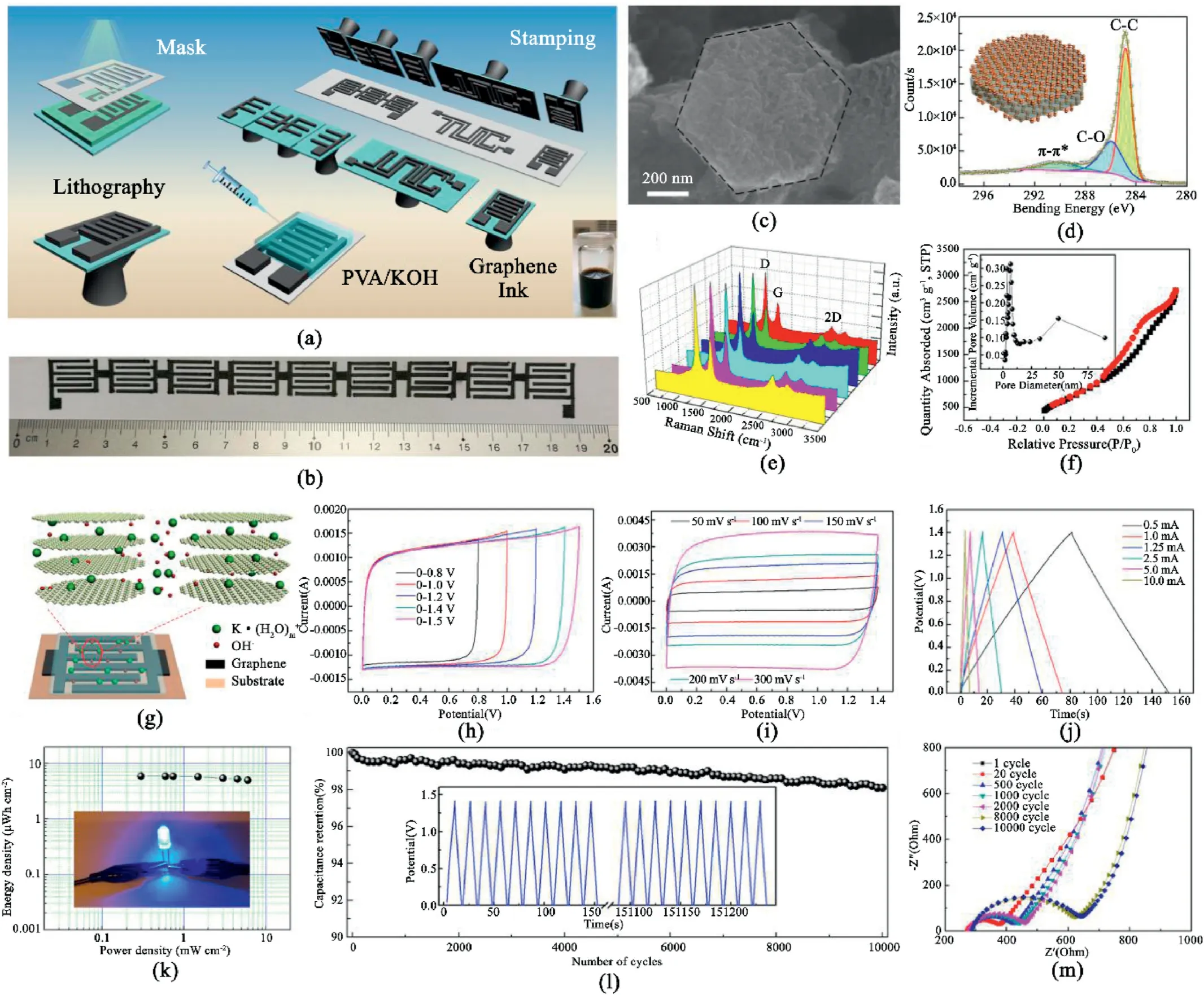
Fig.6.(a)Illustration of the manufacturing process of the stamped MSC devices.(b)Optical image of nine MSCs connected in serial.(c)SEM image,(d)C1s XPS spectrum,(e)Raman spectra,(f)Nitrogen adsorption–desorption isotherms and pore size distribution of the hexagonal graphene.(g)Schematic of charge-storage mechanism.(h–i)CV profiles of different voltages and scan rates.(j)GCD profiles at different currents.(k)Ragone plot and the image of a LED drived by seriallyconnected MSCs.(l)Cycling stability and thefirst andfinal 10 GCD cycles.(m)Electrochemical impedance spectra(EIS)of the devices.Reproduced with permission[76].
The highly porous and conductive graphene used for the stamping ink was synthesized by a template-assisted chemical vapor deposition(CVD)strategy.Hexagonal-shaped porous graphene with high specific surface and outstanding structural stability can be preparedviaCVD grown with porous hexagonal MgOtemplate.Fig.6c–f illustrate the morphology and structure by scanning electron microscope(SEM),X-ray photoelectron spectroscopy(XPS),Raman and Brunauer-Emmett-Teller(BET)test.
The electrical performance of the paper-based symmetric MSCs was tested in PVA/KOH gel electrolyte(Fig.6g–m).Fig.6h displays the cyclic voltammogram(CV)profiles at various voltage windows of the graphene MSC device.A voltage of 0–1.4~V was employed as optimal operating window as shown in Fig.6i.The rectangular CVshapes indicate the doublelayer capacitive behavior of the flexible graphene electrodes.The interdigital MSC devices display remarkable capacitances(22.5 mF cm-2at 300 mVs-1)and outstanding rate capability,which is attributed to the good electrical contacts between active materials and paper substrate,high specific surface area(2326 m2g-1)and excellent conductivity(170 S cm-1)of the graphene.Additionally,the MSC devices demonstrate high energy density of 5.9μWh cm-2at a power of 0.3 mWcm-2and excellent longterm cycling stability(98.8%after 10000 cycles)within 0–1.4 V.
3.3.Flash foam–assisted stamp printing
A facile and straightforward laser-engraved flash foam-inspired stamping technology was employed to prepare flexible planar MSCs[125,126].Flash foam material is mainly formed by polyethylene,which possesses a lot of microbubbles with diameter of tens of microns.Flash foam swiftly absorbs the photon energy when irradiated by high power laser or bright light.In consequence,the surface temperature rises simultaneously,reaching the melting point of flash foam.After laser irradiation or exposure,the temperature of the foam surface reduces rapidly,thus forming a sealed micro-porous surface.The sealed surface of the laser irradiation area isolates the penetration of the oily material.Ground on the property,the as-designed patterns can be efficient transferred to fabricate flash foam-assisted stamps using laser irradiation or exposure.Oily materials absorbed in the unsealed microporous surface were then stamped onto the desired substrates to obtain the pre-designed patterns.
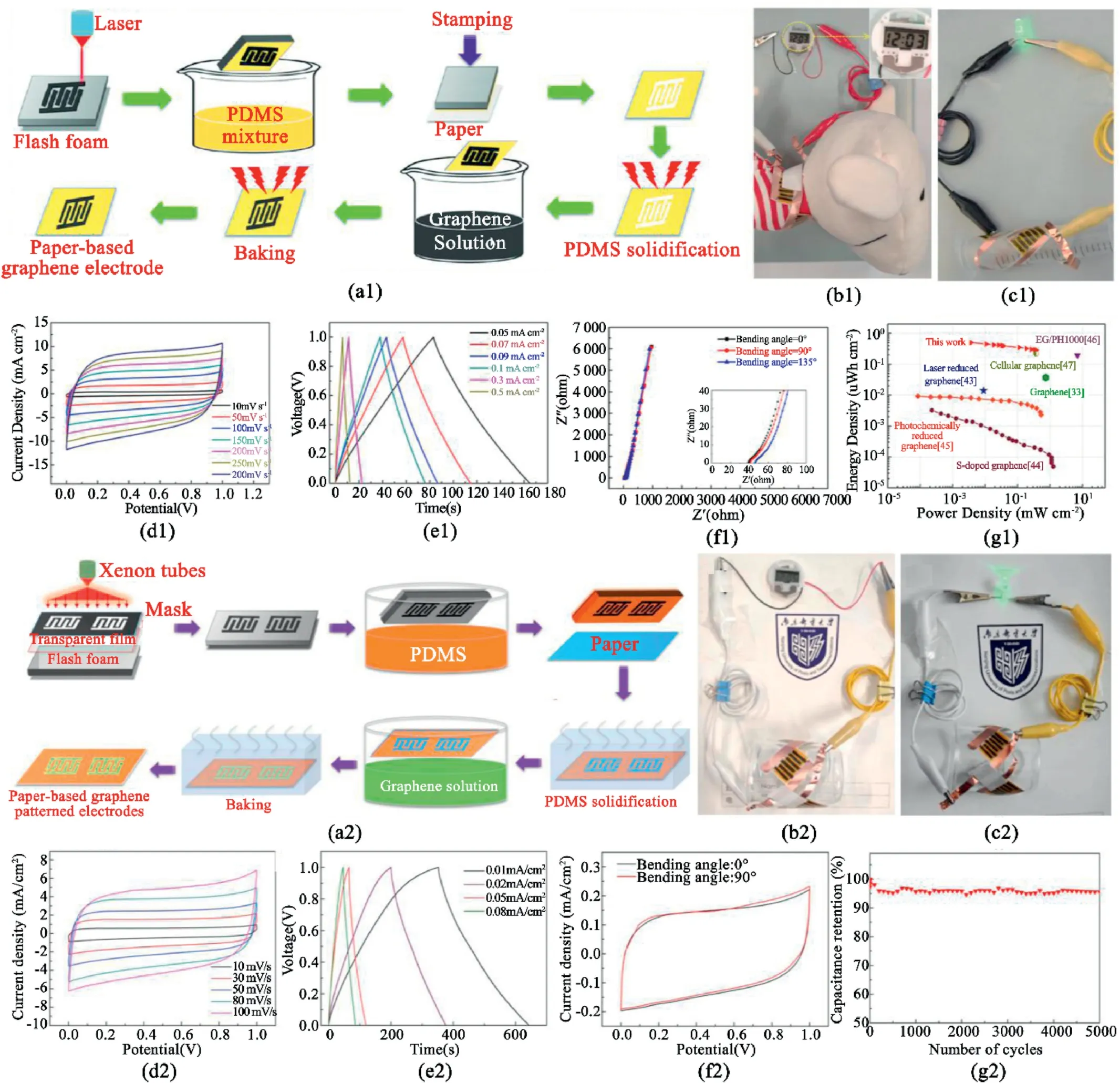
Fig.7.(a1)Schematic diagram of the laser-engraved flash foam-assisted method.Flexible applications of(b1)a commercial watch and(c1)a green LED drived by series-connected MSCs.(d1)CV curves between 0 and 1 V.(e1)GCD curves at various current densities.(f1)EIS tests of the device.The inset is the low-frequency region.(g1)Ragone plot of the MSCs.Reproduced with permission[127].(a2)Diagram of flash foam stamp-assisted manufacturing process.A commercial watch(b2)and a green LED(c2)drived by series-connected MSCs.(d2)CV profiles and(e2)GCD profiles under different condition.(f2)CV profiles before and after bending.(g2)Cycling stability with 0.08 mA cm-2.Reproduced with permission[128].
Zhao et al.prepared flexible paper-based interdigital MSCs with electrochemically exfoliated graphene (EEG) using the flash foam–assisted stamp technique[127].The manufacturing process is shown in Fig.7a1.Firstly,the pre-designed micro-electrode patterns were transferred to a customized laser engraving machine.The subsequent laser engraving make the microporous foam surface closed caused by the thermal fusion.Accordingly,the oily materials cannot penetrate inside the foam of the locked area.Then as-prepared stamp was immersed in the polydimethylsiloxane(PDMS)mixed solution(10 g PDMS of and 1 g of curing agent)for 10 min.Then,the interdigital-patterned stamp was pressed on a paper substrate;therefore,the mixture absorbed in the uncarved foam area was transferred onto the flexible paper.After drying and immersing in EEG and dimethylformamide(DMF)dispersion mixture,the EEGsolution was adhered to the area without PMDS.At last,the EEG-based MSC on flexible paper was obtained after the ink was dried.The as-synthesized graphene MSCs show good electrical properties with high areal capacitance of 3.1 mF cm-2,and good cycling performance of 95.8%retention after 10 000 cycles(Fig.7d1-g1).In addition,the energy densities were 0.5μWh cm-2and 0.3μWh cm-2at current densities of 0.01 mA cm-2and 1 mA cm-2,respectively.
The same group further prepared all-solid-state graphene-based planar MSCs on paper substrate with PVA/H2SO4gel electrolyte[128].They used a similar flash foam–assisted stamping method with predesigned patterned masks.As shown in Fig.7a2,the graphene electrode with desired patterned was obtained after exposure,coating PMDS,stamping on paper,immersing in EEG inks and drying.These newly graphene-based planar MSCs demonstrate outstanding electrical performance with remarkable areal capacitance of~4.02 mF cm-2and long cycle-life(95.6%retention after 5000 cycles)(Fig.7d2-g2).
The main advantages of the laser-engraved flash foam-inspired stamping technology are that it can rapidly transfer desired patterns for large-scale fabrication without complex photolithography patterning orfixed shaped stencils/masks,which is helpful to simplify the fabrication process,decrease costs,and enhance efficiency.
3.4.Stamp-assisted printing
Different from the stamping methods described above,stamp-assisted printing is a method that combines the stamping process with some existing photolithography,deposition,and printing technologies,thereby reducing manufacturing costs and simplifying the manufacturing process.
Khosravi and co-workers fabricated flexible graphene-based MSCs by stamping conductive sublayer and electrodes and brushing active materials[129].As illustrated in Fig.8a–c,three layers of parafilm were prepared on a cleaned PET flexible substrate by stretching process,which is helpful to achieve the interdigitalfingers with suitable depth.Subsequently,silicone-based stamps with desired pattern were coated by Ag or graphite materials and imprinted on the parafilm to create the conductive sublayer as well as the external MSC electrodes.After brushing active material,drying at RT,and cast-coating PVA/H2SO4gel electrolyte,the planar MSC can be achieved.Fig.8d–i show three geometries of MSC devices based on interdigital electrodes.The graphene-based MSC device displays high areal capacitance and large energy density of 8.7 mF cm-2and 6 mWh cm-3.Moreover,the MSC shows good cycling property of 85%retention of capacitance after 25 000 cycles.The stamp-assisted preparation is a facile and low-cost method for high-performance flexible planar MSC devices(Fig.8j–p).
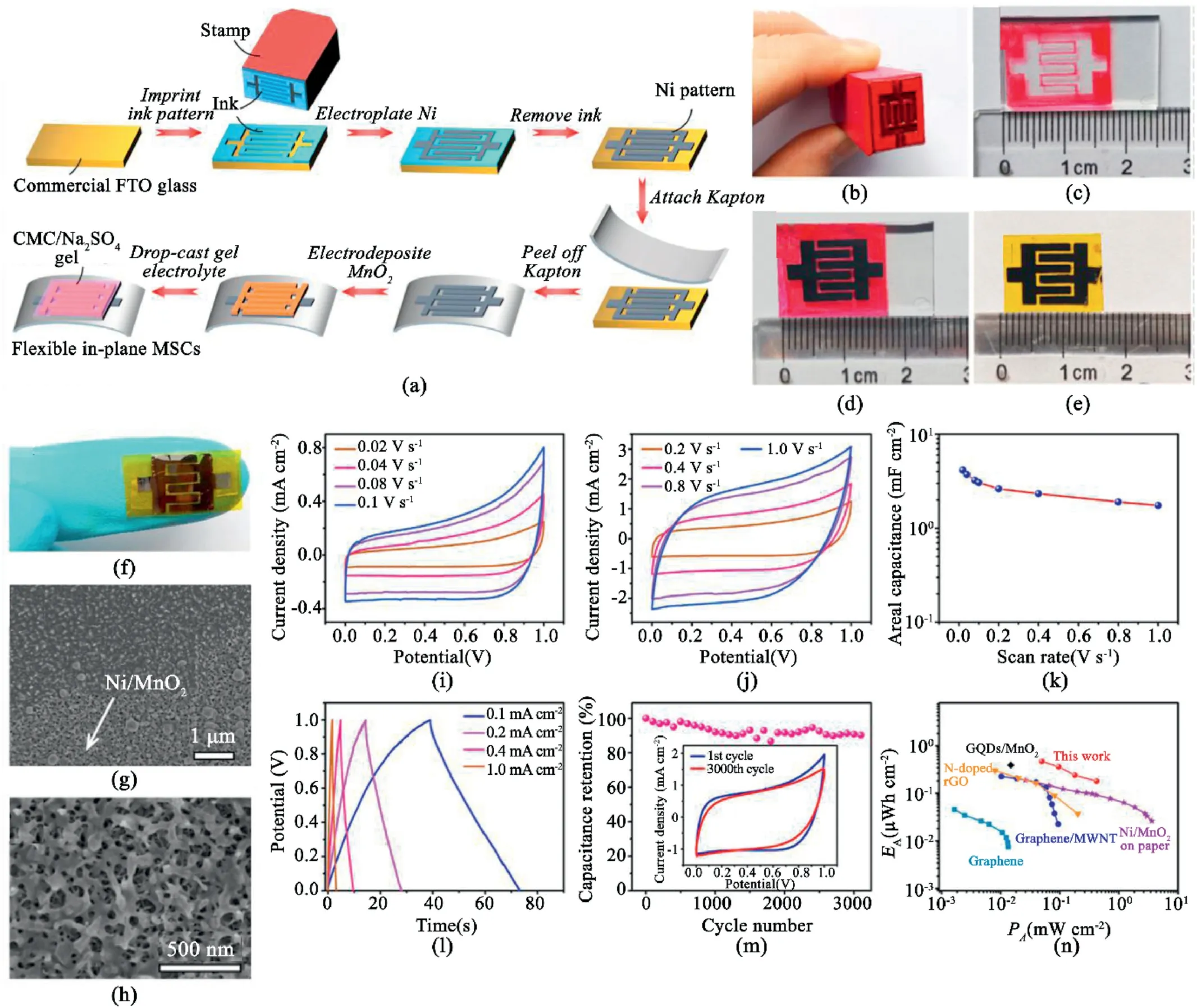
Fig.9.(a)Illustration of the stamp-assisted printing steps of MSC devices.Optical images of(b)stamp,(c)ink pattern,(d)Nifingers on FTO glass,and(e)Nifingers on Kapton.(f)A MSC device on afinger.(g–h)SEM images of Ni/MnO2 electrode materials.(i,j)CV profiles at various scan rates.(k)rate capability.(l)GCD profiles under various current densities.(m)Cycling property.The inset displays CV tests of thefirst and 3000th cycles.(n)Ragone plot.Reproduced with permission[130].
Chen et al.demonstrated a simple and efficient stamp-assisted print fabrication for interdigital in-plane MSCs[130].As shown in Fig.9a,a stamp was hand-pressed on a fluorine-doped tin oxide(FTO)glass substrate to create an interdigital ink pattern.The insulating ink was used as a mold for the subsequent Ni electroplating,preventing the Ni growth on the ink-covered area.Hence,the interdigital pattern of the stamp can be easily mirrored on the FTO substrate,forming Ni interdigital electrodes.After removing the ink mold and transferring the Nifingers form FTO to a flexible Kapton substrate,flexible interdigital Ni electrodes on the Kapton substrate can be successfully achieved.Notably,after these steps the FTO glass remains clean and can be utilized repeatedly.Fig.9b–e show the optical images of the patterned stamp,the imprinted ink mold,Nifingers patterned on FTO glass and on flexible Kapton substrate.Afterwards,flexible in-plane MSC devices werefinally fabricated by electrochemical depositing of MnO2and drop-coating the sodium carboxymethylcellulose(CMC)/Na2SO4gel electrolyte.The as-prepared MSCs show high areal capacitance(4.15 mF cm-2at 0.02 V s-1),outstanding rate capability,good cycling stability(90.3%capacitance retention after 3000 cycles)and high areal energy density(0.18–0.47μWh cm-2)(Fig.9i–n).
It is worth noting that the ink is cheap and the stamp is the stamp is reusable.In addition,the stamp-assisted manufacturing of ink mold is simple and efficient without complex and expensive steps,such as laser scribing and photolithography.Therefore,the stamp-assisted printing technology produces flexible devices with low-cost and accessible operations,which offers a new way for the manufacture of flexible in-plane MSC devices.
4.Properties of stamped MSCs
Similar to ordinary printing methods,the substrate for stamping is usually flexible paper,PET substrate,leaves,carbon cloth,woven fabric,etc.Accordingly,the imprinted MSC devices generally possess excellent mechanical properties,such as flexibility and bending stability.In addition,the stamp printing method is simple and highly repeatable.Therefore it is easy to realize large-scale preparation of MSCs and the series and parallel connection of multiple capacitors through various stamp design,such as pad or cylindrical stamps.The merits of the stamping method open new stimulating opportunities for wide applications in portable and wearable electronics.In this section,we introduce the superiority of the stamped MSC devices.

Fig.10.(a1)Optical image of graphene-based MSCs with 4×11 array on PET substrate.(b1)Relative capacitance of 1000 charge/discharge cycles,and(c1)1000 bending cycles.(d1,e1)Diagram of the two bending states.Reproduced with permission[101].(a2)Diagram for inside and outside bending.(b2-c2)Optical images of MSC devices bent inside and outside the substrates.(d2)CV profiles under different bending deformations.Reproduced with permission[130].(a3)I–Ti3C2Tx MSCs on the PETfilm.(b3)Resistance change as a function of the bending angles.Insets show optical images of the bending devices.(c3)CV curves of I–Ti3C2T x under various bent states.Reproduced with permission[109].(a4)Schematic diagram of the bending state.(b4,c4)Optical images of bending supporters with various diameters.(d4-f4)Optical images of bending MSCs with bending radii from 1.5 to 5 mm.(g4-h4)CV profiles under different bending radii(g4)and angles(h4);(i4)Capacitance retention after different bending cycles.Reproduced with permission[76].
4.1.Flexibility
With the speed development of portable,wearable,and foldable electronic devices,the requirement for flexible ESDs has also been further amplified.Accordingly,printed MSCs are increasingly used in integratable devices due to their inherent flexibility,and researchers are paying more and more attention to the mechanical performance testing of flexible devices[131–133].
For example,in Hyun's work,the flexible graphene MSCs exhibit outstanding flexibility[101].In Fig.10a1–e1,two types of bending modes were studied:bending the MSCs inside and outside the PET substrate with a bending radius of 1 cm.After 1000 bending cycles,the areal capacitance remains almost unchanged with both the inside bending and outside bending.The remarkable bending cycling stability is mainly caused by the deformable property of the ion gel electrolyte and good mechanical flexibility of the graphene electrodes.
Chen et al.also performed the bending test with two different directions to test the mechanical tolerance against bending:outside bending and inside bending,in which the devices suffer from tensile strain and compressive strain,respectively,as illustrated in Fig.10a2-d2[130].The devices can endure strong inside and outside bending deformation(Fig.10b2-c2),indicating remarkable flexibility attached on a curvy humanfinger,similar with an electronic skin.The CV curves display a negligible change when the device undergo inside bending and outside bending at various bending radiuses(Fig.10d2),suggesting the desirable flexibility of the MSC devices.
Gogotsi's group stamped MXene inks onto both surface-treated PET and paper[109].As shown in Fig.10a3,the paper-based I–Ti3C2TxMSC devices show good flexibility under repeated bending/releasing.The CV curves changes slightly(<20%)under different bending angles in Fig.10c3.In addition,the capacitance retains 85%of the initial value after 1600 bending cycles,demonstrating the enormous potential for the applications of wearable and portable electronics(Fig.10c3).
Li et al.performed systematic bending tests to examine the mechanical performance of the flexible graphene MSCs[76].Both bending radius(r)and bending angle are utilized to characterize the flexible property(Fig.10a4–f4).The shapes of the CV curves under different bending radius from 1.5 mm to 5 mm and different bending angles range from 0–180°maintain almost unchanged and display negligible capacitance fluctuations(Fig.10g4-h4),suggesting remarkable electrical stability and mechanical flexibility.Fig.10i4 shows the cycling performance of the device under continuous bending cycles.The capacitance remains~83.5%of the initial value after 300 bending cycles.The outstanding mechanical property is probably due to the flexible nature and porous surface of the graphene electrode,the well-designed device pattern,and the good integrity of the electrodes and interconnects.
4.2.Mass production and tailoring properties
Stamping is an effective strategy to further decrease the preparation period and production costs.For example,the production of Ti3C2TxMSC devices can be efficient scaled up by cold rolling processes with cylindrical or pad stamps.Zhang and co-workers fabricated handle attached cylindrical stamps with interdigitatedfingers to promote the cold rolling.As a result,dozens of I–Ti3C2TxMSCs can be promptly stamped in seconds[109].
To fulfill the requirement of electronics for practical application,fabricating integrated ESDs with tailored capacitance and voltage output is imminently demanded.For example,three devices in parallel and series configuration were developed and studied by GCD curves in Woo Jin Hyun's work[101].Fig.11a1-b1 show diagrams of the circuit and photograph of integrated MSC devices.Compared to a single device,the widened potential window of the series configuration(Fig.11c1)and the improved discharge time of the parallel configuration(Fig.11d1)are increased by a factor of three.
Chen et al.demonstrated the preparation of the series-and parallelconnected MSC devices in Fig.11a2[130].By designing smart stamp shapes,the interconnected ink mold and serial-and parallel-connected Ni metalfingers were readily produced.Three in-plane MSC devices in series and parallel without extra conductive wires were integrated on Kapton(Fig.11b2-c2),demonstrating extended potential window and approximately triple GCD time,respectively.The stamp-assisted printing of MSCs without external conductive wires offers remarkable feasibility for facile and efficient integration of microelectronics.
In Zhao's work,four devices in series and parallel were integrated to demonstrate the scalability of the planar EEG-MSCs[128].As expected,four devices in series and in parallel(Fig.11a3-b3)display extended operating window and output current,respectively,which are approximately four times larger than a single MSC.In addition,the GCDcurves of both connection types maintain the triangular shape with a small IR drop in Fig.11c3-d3.
Similarly,Li et al.develop rapid and scalable stamping fabrication for large-scale production of the integrated MSC devices[76].Notably,the CV profiles and GCD curves of one tofive devices in series(Fig.11 a4-b4)demonstrate stepwise increase of the potential windows from 1.4 V to 7.0 V,suggesting highly uniformity.Moreover,the output current of the CV curves and the discharge time of the GCD profiles of the devices in parallel increase linearly(Fig.11 c4-d4).
Through the introduction above,the stamping ink of the MSC such as the graphene and MXene ink often possess remarkable conductivity,high electrical property,and good rheological natures.It is foreseen that these conductive inks can be utilized simultaneously for electrodes and interconnects for mass manufacturing of MSC devices.The scalable fabrication of these integrated MSCs indicates the great potential for microelectronics industry.
5.Summary and outlook
Stamp printing of MSCs is an emerging flexible device manufacturing technology,which has enormous potential in the next generation of wearable and flexible microelectronics.In this review,we discussed the active materials commonly used for stamp printing and the required characteristics of stamping inks,among which graphene and MXene materials with excellent conductivity,good hydrophilicity and stable electrochemical performance are of immense interest.Then,several different stamping methods are further demonstrated,including gravure printing,letterpress printing,flash foam–assisted stamp printing and stamp-assisted printing.Each printing method has its preparation processes,suitable inks,and their printed devices possess different electrochemical properties.Finally,the advantages of stamping MSCs are emphatically discussed.The current flexible electronics industries all urgently need excellent mechanical properties,large-scale manufacturing,and performance customization.Accordingly,stamping MSC devices are anticipated to play a crucial part in ESDs and are beneficial to accelerate the progress of portable microelectronics.

Fig.11.(a1-b1)Diagram of the circuit and photograph of three devices connected in series and parallel.(c1-d1)GCD curves for three devices in series and parallel configuration.Reproduced with permission[101].(a2)Illustration of the manufacturing of integrated MSC arrays in series and parallel.(b2-c2)Optical images of the integrated MSCs.(d2)CV profiles of three devices in series.(e2)GCD profiles of three devices in parallel.Reproduced with permission[130].(a3-d3)The CV profiles and GCD curves of four devices in parallel and series.Reproduced with permission[128].(a4)CV curves and(b4)GCD curves of MSC devices connected in series.(c4)CV curves and(d4)GCD curves of MSC devices connected in parallel.Reproduced with permission[176].
In spite of these achievements,stamping devices has not become a mature technique.Several challenges need to be tackled for wide applications,including integration with solar cells to build a self-powered configuration to store solar energy,acting as power sources to drive external electronic components.
First,the stamp printing resolution(200μm)and overlay accuracy are much lower compared to conventional micro-fabrication methods(sub-one micron for photolithography and Electron beam lithography)[41,134–136].Hence,well-designed stamps,ink materials,substrates,and processing technology are needed to enhance stamping resolution and accuracy.
Second,gaps still exist in electrical property between stamped materials(~100 mF cm-2)and functional materials in situ grown and synthesized on desired substrates(more than 1 F cm-2)[137–142].Therefore,more imprinting ink materials with high conductivity and hydrophilicity should be synthesized to explore the suitable physical stamping properties and improve the electrical performance.In addition,the stamping devices are intensively expected to integrate versatile materials with different properties for enriching the functionalities,which are responsive to external stimuli,such as temperature,mechanical deformation,voltage and light.
Finally,a variety of methods have been developed to achieve planar high-performance MSCs with submillimetre-scale features(a footprint area of less than 1 cm2)[135,143–148].One effective strategy is to increase stamping electrode thickness within afixed small footprint(less than the 1×1 cm2)without sacrificing other stamping properties like process yield and throughput.
Declaration of competing interest
None.
Acknowledgments
F.L.and Y.L.contributed equally to this work.F.L.,Y.L.,J.Q.and J.W.acknowledge the support and funding from China Scholarship Council(CSC).O.G.S.acknowledges support by the Leibniz Program of the German Research Foundation(SCHM 1298/26-1).
杂志排行
Namo Materials Science的其它文章
- GUIDE FOR AUTHORS
- Editorial for a special issue“Nano energy materials and devices for miniaturized electronics and smart systems”
- Aim & Scope
- Low-power emerging memristive designs towards secure hardware systems for applications in internet of things
- A comprehensive review of miniatured wind energy harvesters
- Advanced architecture designs towards high-performance 3D microbatteries