Advanced architecture designs towards high-performance 3D microbatteries
2021-07-28YangLiJiangQuFeiLiZheQuHongmeiTangLixiangLiuMinshenZhuOliverSchmidt
Yang Li ,Jiang Qu ,Fei Li ,Zhe Qu ,Hongmei Tang ,Lixiang Liu ,Minshen Zhu ,Oliver G.Schmidt ,d
a Material Systems for Nanoelectronics,Chemnitz University of Technology,09107 Chemnitz,Germany
b Institute for Integrative Nanosciences,Leibniz IFW Dresden,01069 Dresden,Germany
c Center for Materials,Architectures and Integration of Nanomembranes(MAIN),Chemnitz University of Technology,09126 Chemnitz,Germany
d School of Science,Dresden University of Technology,Dresden,01062,Germany
Keywords:Microbatteries Origami technologies Rolled-up nanotechnology 3D devices Energy storage performance
ABSTRACT Rechargeable microbatteries are important power supplies for microelectronic devices.Two essential targets for rechargeable microbatteries are high output energy and minimal footprint areas.In addition to the development of new high-performance electrode materials,the device configurations of microbatteries also play an important role in enhancing the output energy and miniaturizing the footprint area.To make a clear vision on the design principle of rechargeable microbatteries,wefirstly summarize the typical configurations of microbatteries.The advantages of different configurations are thoroughly discussed from the aspects of fabrication technologies and material engineering.Towards the high energy output at a minimal footprint area,a revolutionary design for microbatteries is of great importance.In this perspective,we review the progress of fabricating microbatteries based on the rolled-up nanotechnology,a derivative origami technology.Finally,we discussed the challenges and perspectives in the device design and materials optimization.
1.Introduction
Miniaturizing energy storage devices to the microscale is a critical challenge for the development of next-generation electronic devices.Thereinto,rechargeable microbatteries(rMBs)have attracted tremendous attention due to their advantages of high energy density and long cycle life[1–3].Based on different battery chemistries,rMBs can be divided into several categories,among which lithium-ion,sodium-ion,and zinc-ion rMBs dominate[2,4–7].Regardless of the battery chemistry,prototypes of rMBr share a basic thin-film configuration(Fig.1)[8–20].The thickness of batteries should be controlled at the microscale,thus meeting the standard of dimensions for rMBs.However,the limited thickness of the electrode limits the output energy of the rMB.Benefiting from new techniques of engineering materials to 3D porous structures,the output energy of rMBs increases rapidly.In addition to the significant progress in improving the output energy of rMBs,the adaptability to next-generation electronic devices,such as flexible and wearable electronic devices,gradually becomes an essential requirement of rMBs.These new requirements further raise the challenge in device design,materials engineering,and battery chemistry.
When it comes to the design of a rMB,two basic architectures are available:sandwiched(Fig.2a)[21–26]and interdigital(Fig.2d)[27–29]structures.These two architectures are highly compatible with microfabrication technologies,such as photolithography and printing technologies.Besides the design,pursuing high energy density is the core challenge for rMBs.An intuitive way to improve the energy density is to increase the thickness of electrodes because the energy density of a rMB is proportional to the mass loading of electrode materials(Fig.2b and e).Nevertheless,a long charge transfer pathway accompanies with a large electrode thickness,which impairs the performance at a high current density and cycling stability due to cracks upon repeatedly electrochemical reactions.To tackle this issue,dense structures evolve to discrete structures.For the sandwiched structure,it can be split into a microelectrode array(Fig.2c).This strategy increases the surface area that can be used to load electrode materials while it maintains the low thickness of electrode materials.The same strategy can also be applied to the 2D interdigital architecture(Fig.2f).Thick interdigital microelectrodes can be broken down to nanorod arrays,which show the large thickness and short charge transfer pathway due to the high aspect ratio of each nanorod electrode.As a result,the transformation of 2D structures to 3D hierarchical structures have effectively improved the energy density,rate performance,and cycling stability of rMBs[20,30–36].
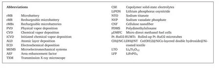

Fig.1.A brief timeline of the development history of representative 3D rMBs.Inset images:i is reprinted with permission from Ref.[8],Copyright(2000)Elsevier.ii is reprinted with permission from Ref.[9],Copyright(2000)IOPscience.iii is reprinted with permission from Ref.[10],Copyright(2007)Institute of Electrical and Electronics Engineers.iv is reprinted with permission from Ref.[11],Copyright(2007)Elsevier.v is reprinted with permission from Ref.[12],Copyright(2013)The Royal Society Of Chemistry.vi is reprinted with permission from Ref.[14]Copyright(2013)Nature Publishing Group.vii is reprinted with permission from Ref.[13]Copyright(2015)National Academy of Sciences.viii is reprinted with permission from Ref.[20]Copyright(2018)WILEY-VCH.ix is reprinted with permission from Ref.[15]Copyright(2018)American Chemical Society.x is reprinted with permission from Ref.[18]Copyright(2019)American Chemical Society.xi is reprinted with permission from Ref.[16]Copyright(2019)WILEY-VCH.xii is reprinted with permission from Ref.[17]Copyright(2019)WILEY-VCH.xiii is reprinted with permission from Ref.[19]Copyright(2019)WILEY-VCH.
In terms of the integration into microelectronics,a minimal footprint area is an essential requirement.However,the above architectures are technically based on 2D designs.If the footprint area is significantly reduced,the output energy will decrease dramatically as the mass loading of electrode materials reduces.Meanwhile,rMBs consist of multilayered structures and highly active materials that can be easily damaged by the environment.As a result,it is extremely difficult to fabricate the rMB at a sub-millimeter area by adopting conventional 2D designs.An effective strategy realizing a rMB that has high energy density and occupies a minimal footprint area could be the transformation of a 2D device into a 3D device,which can take the advantages of the microfabrication for a 2D device and mature engineering technologies for the hierarchical electrode design.Fig.2g–j shows technological routes towards a 3D device by a derivative origami technology.The shape transformation is triggered by the release of the intrinsic strain in layered materials.Based on this mechanism,almost all 2D rMBs can be used for origami rMBs,which substaintially expands choices for the design of rMBs.The discrete electrode design also broadens mateirals choices.Combining these two advantages,the origami rMBs are promising to accomplish the goal of sufficient output energy at a minimal footprint area.
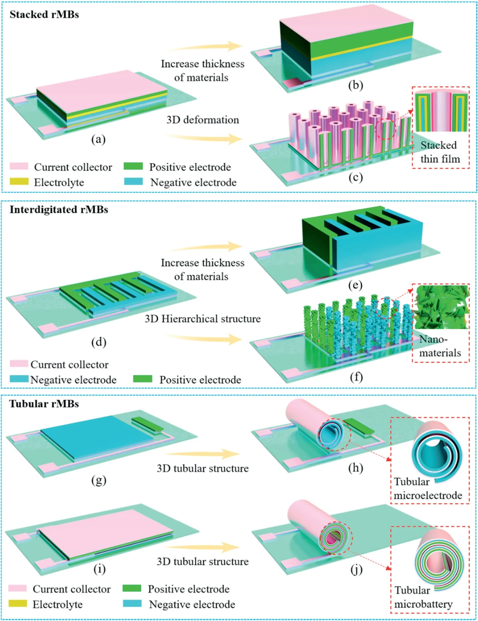
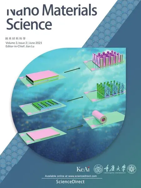
Fig.2.Schematic of different configurations for rMBs.(a–c)Sandwiched rMBs,(d–f)Interdigital rMBs.(g–j)Origami rMBs.
2.3D sandwiched architecture
To develop a 3D sandwiched rMB,the electrode host should be engineered to a 3D structure,such as microchannels[37],micro/nanopillars[38],and vertical microtubes[39].The logic behind this engineering process is to increase the surface area that can load electrode materials.Area enhancement factor(AEF)is derived to guide 3D engineering.For a rMB,the AEF refers to the ratio between electrochemically active surface area and the footprint area of a 3D rMB.Eustache et al.investigated the relationship between AEF and the energy storage ability of the rMB assembled by a microtube array(Fig.3a)[40].The AEF can be precisely controlled by the inner depth of the microtube(Fig.3b).With an AEF value of 100,the areal capacity of a TiO2anatase polymorph based rMB is around 100 orders of that for a rMB with an AEF value of 1(Fig.3c).In addition to the AEF value,the thickness of the electrode determines the output energy at a limited footprint area of a rMB.As shown in Fig.3c,the area capacity increases with the increasing thickness of the electrode.L′etiche et al.fabricated a 3D Li-ion rMB assembled by micropillars(Fig.3d–f)[41],which delivered a high area capacity of 370μA h cm-2,reaching around 100 times higher capacity than that of a planar device(3.5μA h cm-2,Fig.3g).Accordingly,a high area capacity builds on the deliberately optimized AEF and thickness of the electrode of the rMB.The same strategy can be adapted to rMBs with different electrode materials.A vanadium dioxide(VO2)thinfilm(40 nm)was deposited on silicon micropillars(AEF=21),and the resulted rMB showed an area capacity of 130μA h cm-2[42].The specific capacity of the rMB with a 1-μm-thick MoOySzreached up to 2 mA h cm-2[43].In addition to the deposition of electrode materials on a 3D silicon host,the silicon is a high-capacity anode material for lithium ion batteries.As shown in Fig.3h–k,a 3D silicon micropillar array boosts the area capacity to 1.8 mA h cm-2[44].The 3D silicon-based rMB also showed a very good cycling performance(100 cycles at 0.56 mA h cm-2)at a high current density of 0.66 mA cm-2.

Fig.3.(a)Structure overview of a 3D Li-ion rMB.(b)Evolution of AEF as a function of the inner depth in the silicon microtubes.(c)Calculated surface capacity of a TiO2 anatase layer as a function the TiO2 thickness and the AEF of the 3D scaffold.Reprinted with permission from Ref.[40]Copyright(2014)WILEY-VCH.(d)Scanning electron microscopic(SEM)image of the 3D silicon scaffold.(e–f)Transmission X-ray microscope(TXM)images of a silicon micropillar coated with the four functional layers(Al2O3,Pt,TiO2,and Li3PO4 thinfilms)deposited by atomic layer deposition(ALD).(g)The surface capacity of the 3D silicon scaffold regarding the state-of-the-art rMBs.Reprinted with permission from Ref.[41]Copyright(2017)WILEY-VCH.(h)SEM image of silicon array.(i)SEM image of a full 3D battery.(j)Charging schematic of the 3D battery.(k)Cycling performance of a full rMB at a charge/discharge current of 0.22 mA cm-2/0.11 mA cm-2.Reprinted with permission from Ref.[44]Copyright(2018)Elsevier.
From the engineering view,plenty of tehcniques are available for the micromachining of a 2D structure to a 3D structure.For example,the dry etching technique of silicon can successfully transform a silicon wafer into a silicon micropillar array[44].Besides,a 3D copper host with a vertically aligned nanopillar array[45,46]and 3D TiO2nanopillars[40]were developed as the 3D electrodes.The deposition of electrode materials onto the 3D electrode hosts are realized by various deposition techniques,such as ALD[47–55],chemical vapor deposition(CVD)[56–58],and physical vapor deposition(PVD)[59–77].Gregorczyk et al.developed a 3D solid-state battery by ALD(Fig.4a)[15].Functional layers of the rMB were deposited into the microchannel,which established a high quality and dense multi-layered structure and hence enabled the stable operation of the rMB.By changing microchannels to nano/micropores,an all-in-one rMB was realized(Fig.4b),in which V2O5is the electrode material[78].Thanks to the porous feature of the 3D electrode,the electrolyte can be infiltrated into nanopores.The as-developed all-in-one rMB delivered the energy density of 3.8μWh cm-2μm-1and the power density of 1012μW cm-2μm-1.The rate and cycling performance of a full battery was also good,demonstrating a great promise in practical applications.Despite the good compatibility with deposition techniques,the choices of electrolytes are highly limited.Normally,solid-state electrolytes are used due to their high compatibility with variant deposition methods.However,the low ionic conductivity of the solid-state electrolyte largely impedes the pursuit of the high output energy of rMBs.Therefore,it is of great importance to integrate alternative electrolytes with high ionic conductivity into rMBs.Li et al.developed a copolymer solid-state electrolyte(CSE)viainitiated chemical vapor deposition(iCVD)[35].3D TiO2electrodes were used as the template for the deposition of the copolymer thinfilms(Fig.4c).The broad tunability of the ionic conductivity of the copolymer electrolyte was achieved by optimizing the cross-linking density and matrix polarity.The optimized ionic conductivity at the room temperature reached(6.1±2.7)×10-6S cm-1,which is much better than the widely used lithium phosphorus oxynitride(LiPON)(~10-7S cm-1).

Fig.4.(a)Fabrication and characterization of a 3D solid-state rMB.Reprinted with permission from Ref.[15]Copyright(2018)American Chemical Society.(b)i,schematic of parallel nanopore battery array;ii,schematic of the cross-section of a single-pore battery;iii,rate performance the full-cell device.Inset:charge and discharge curves at the second and 1,000th cycles.Reprinted with permission from Ref.[78]Copyright(2014)Nature Publishing Group.(c)i,a schematic illustration of the CSE preparation and the conformal coating of copolymers on 3D substrates;ii,the impedance spectroscopy of the fabricated CSEs.Reprinted with permission from Ref.[35]Copyright(2019)American Chemical Society.
For 3D sandwiched rMBs,several engineering hurdles,such as the complicated design of 3D electrode arrays and complex deposition technologies towards thick and reliable electrodes and electrolytes,plagued the accomplishment of high output energy at a minimal footprint area.In addition,these rMBs are usually fabricated on rigid substrates,which benefits the integration in the on-chip electronic devices but impairs the feasibility of the application in next-generation electronic devices with high flexibility and wearability.
3.3D interdigital architecture
Transforming a dense and bulky sandwiched structure into a 3D microstructure assembly has proven its efficiency in improving the output energy of a sandwich-structured rMB.Nevertheless,such 3D sandwiched architecture still faces the limitation of electrode thickness because the interfacial stress between different layers will result in the failure of the rMB.To tackle this challenge,3D interdigital architectures have been developed.The anode and cathode in a rMB are placed on the same plane and spaced out with a micrometer gap.Early prototypes of 3D interdigital rMBs mimic the structure of 3D sandwiched rMBs:an array of interdigital cylindrical microelectrodes is fabricated[79].Then,the structure evolved into the array of interdigital plates,and becomes a dominant design[80–84].When the cathode and anode are separated in the same plane,we are able to push the thickness of each electrode.Meanwhile,porous structures can be engineered to enable intimate contact between electrodes and electrolyte,thus enhancing the energy storage ability.Periodically mesostructured 3D lattice was designed by 3D holographic lithography and 2D photolithography(Fig.5a)[13].Ni was then grown on the mesostructured template as the current collector for the rMB.Afterwards,Ni-Sn and lithiated MnO2were sequentially deposited onto the Ni coated template.Thanks to the large thickness of microelectrodes and porous structure,a high energy density of 6.5μWh cm-2μm-1and an impressive power density of 3600μW cm-2μm-1were achieved.To further improve the output energy of a rMB,a straightforward way is to increase the porosity.Pikul et al.developed a 3D Li-ion rMB based on porous microelectrodes(Fig.5b)[14].Compared to the rMB in Fig.5a,the porosity of microelectrodes is significantly increased.As a result,the energy density increases to 15μWh cm-2μm-1and the maximum power density increases to 7.4 mW cm-2μm-1.Alternatively,a nanoporous structure is effective to improve the energy density[85].KxV2O5·nH2Oand KxMnO2·nH2O are deposited onto the nanoporous microelectrodes(Fig.5c)and assembled into a rMB,which delivered an ultrahigh energy density of 103 mWh cm-3with a supercapacitor-level power density(600 W cm-3).

Fig.5.(a)i,the configuration of 3D interdigital rMB;ii,cross-section SEMimages of the interdigital electrodes.Inset:the magnified electrodes with the nickel scaffold coated with nickel-tin on the left and lithiated manganese oxide on the right;iii,the performance of the fabricated rMB.Reprinted with permission from Ref.[13]Copyright(2015)National Academy of Sciences.(b)i,schematic of interdigital patterns of a 3D in-plane rMB;ii,cross-section SEM images of the interdigital electrodes of 3D lithiated MnO2 cathode(left inset)and Ni–Sn anode(right inset).(b)iii,simulated(lines)and measured(scattered points)capacity as a function of electrode digit width.Reprinted with permission from Ref.[14]Copyright(2013)Nature Publishing Group.(c)i,the schematic illustration of an aqueous K-ion rMB;ii,SEM images of the Kx V2O5 anode and KxMnO2 cathode supported on the nanoporous Au current collectors.Scale bar 200 nm iii,the capacity retention of flexible aqueous rMB at different bending angles.Inset:photographs of a bent K-ion rMB.Reprinted with permission from Ref.[85]Copyright(2019)Nature Publishing Group.
Upon the change of the fabrication route from stacking functional layers to the in-plane manufacturing of the electrodes and electrolyte,choices for electrode materials have been expanded[86–96].For instance,Zheng et al.used sodium titanate(NTO)anode and sodium vanadate phosphate(NVP)cathode with hierarchical nanostructures to assemble a 3D interdigital rMB(Fig.6a and b)[84].The fabricated rMB exhibited a high energy density of 55.6 mWh cm-3at the rate of 1C.Moreover,it exhibited long-term cycling stability,showing a high volumetric capacity of 10.1 mA h cm-3after 3000 cycles at a high rate of 20 C(Fig.6c).It is noteworthy that 3D interdigital rMBs are not limited to rigid substrates,flexible substrates,such as polymer membranes and fabrics can be used,which enables the development of flexible and wearable rMBs[81,82].

Fig.6.(a)Schematic of the preparation of current collectors,NTO anode,and NVP cathode.(b)SEM images of NTO(i)and NVP(ii);cross-section SEM images of the anode(iii)and cathode(iv).(c)Long-term cycling performance of the fabricated rMB.Reprinted with permission from Ref.[84]Copyright(2020)The Royal Society of Chemistry.
3D printing technologies can also be employed to fabricate 3D interdigital rMBs[20,97–101].The thickness of the microelectrode can be precisely controlled by varying printing cycles.Lewis et al.fabricated a 3D interdigital rMB by printing Li4Ti5O12(LTO)and LiFePO4(LFP)inks on gold current collectors[102].The fabrication process of the rMB was completed by sintering and packaging of the printed microelectrodes(Fig.7a–d).Fig.7e depicts the areal capacity of a 3D interdigital rMB as the function of charge/discharge rate.The rMB delivered a high areal energy density of 2.6 mWh cm-2at a power density of 2.7 mW cm-2.As the ink composition is critical for stable and continuous printing,the electrode materials should be deliberately engineered to be compatible with the ink printing process,which,to some extent,sets a restriction of materials choice.To circumvent this problem,a reliable and modifiable template can befirstly printed.For instance,the cellulose nanofiber(CNF)were printed on the substrate,serving as the microelectrode template(Fig.7f)[16].After the carbonization of cellulosefibers into conductive networks,Li metal was infused into the network,forming the microanode.For the microcathode,LiFePO4electrode was printed using a CNF-based ink.The materials loading was controlled by the printing layers(Fig.7g).Consequently,the as-developed rMB exhibited a high capacity of 80 mA h g-1(at a rate of 10 C)and a good capacity retention of 85%after 3000 cycles(Fig.7h).
In addition to the direct design based on deposition and printing technologies,the interdigital microelectrodes can be created by the laser scribing tehcnologies.Mai et al.fabricated a 3D interdigital rMB by using the laser engraving technology[103].Active materials were synthesized on a textile substrate and patterned by the laser engraving.The fabricated hierarchical Co(OH)2@NiCo-layered double hydroxide@Ni-coated textile was cut into an interdigital microcathode.The microanode was fabricated by the similar process.Finally,the microcathode and microanode were transferred to the polydimethylsiloxane(PDMS)template and assembled into an interdigital rMB.The as-developed alkaline rMB delivered a high areal energy density of 0.17 mWh cm-2and the maximum areal power density of 14.4 mW cm-2.

Fig.7.(a)The fabrication flow of 3D interdigital rMB by a printing technology.(b)Optical and(c)SEMimages of the printed and annealed 16-layer interdigital LTOLFP electrode architectures,respectively.(d)The optical image of a 3D Li rMB consisting of LTO-LFP electrodes after packaging.(e)The discharge curve of a full cell consisting of 8-layer interdigital LTO-LFP electrodes.Reprinted with permission from Ref.[102]Copyright(2013)WILEY-VCH.(f)The digital image of pristine CNF gel,CNF ink,CNF/LFP ink,and LFP dispersion stored in inverted vials to show viscosity(left).CNF/LFP electrode printed layer by layer(right).(g)The digital image of dry CNF/LFP electrode printed with different layers from 9 to 21.(h)Long-term cycling performance at 10 C for the full cell with c-CNF/LFP cathode and c-CNF/Li anode.Reprinted with permission from Ref.[16]Copyright(2019)WILEY-VCH.
3D interdigital architectures allow for a large mass loading of electrode materials,and hence effectively improve the output energy of rMBs.Liberated from stacking multilayers into a sandwiched structure,most of electrode materials can be integrated into the 3D interdigital rMBs,which further facilitates the fabrication of high energy rMBs.Moreover,this architecture can be adapted to flexible substrates,which offers the possibility to be integrated with flexible and wearable electronic devices.In spite of these advantages,one hurdle facing by the application in advanced electronic devices is the mismatch between the footprint area of 3D interdigital rMBs and advanced microelectronics.
4.Rolled-up microtubular architecture
As mentioned before,ideal rMBs for next-generation electronic devices require high output energy at a minimal footprint area.The progress of reducing the footprint area of rMBs at a sub-square millimeter level is too slow to match the miniaturization trend of microelectronics.Inspired by the packaging technology of commercial batteries,an effective strategy is to transform a large membrane into a rolled-up structure,which can accomplish the high output energy at a minimal footprint area.At the microscale,it is extremely difficult to precisely control such mechanical transformation by external stimulis.Therefore,rolled-up nanotechnology that utilizes the intrinsic stress in nanomembranes becomes a promising method to answer the challenge.In addition to the high efficiency in reducing the footprint area,the rolled-up nanotechnology can adopt all microfabrication methods elaborated above,envisioning a fast technological transfer towards tiny microbatterires.The rolled-up nanotechnology transforms 2D devices into 3D objects,which resembles the spirally packaged electrodes in a cylinder battery(Fig.8a)[104–108].Due to large active surface areas,fast ion diffusion through the nano-thick membrane,and strain accommodation ability,the energy storage performance of the rolled-up electrode has been considerably improved[109–116].For example,Huang et al.fabricated a 3D TiO2-δnanomembrane anode by the rolled-up technology(Fig.8b),which delivered an area capacity of 100μA h cm-2and showed an ultralong lifespan over 5000 cycles without capacity decay[117].Likewise,rolled-up Si/rGO bilayer nanomembranes were designed and exhibited a long cycling lifetime of 2000 cycles with the capacity of 571 mA h g-1at 3 A g-1.The rolled-up nanomembranes can be further used as a freestanding electrode for the rMB.Tang et al.fabricated a unique Si–Ge spiral microelectrode(sp-μED)for a high-performance lithium-ion rMB(Fig.8c)[118].The interlayer gap and nanomembrane of each winding enable a fast charge transfer,which perfectly resolves the disadvantage of sluggish charge transport in thick microelectrodes(Fig.8d–f).The capacity of Si–Ge sp-μED increases by 9 times compared to the nanomembrane electrode(Fig.8g and h).The dramatic increase in areal capacity proves the effectiveness of the enhancement of energy density by the spiral structure.

Fig.8.(a)The schematic illustration of the rolled-up process.Reprinted with permission from Ref.[104]Copyright(2001)Nature Publishing Group.(b)Ultra-stable performance of TiO2-δ/Ti nanomembranes at 10 C over 5000 cycles.The inset shows the ultrathin nanomembranes and the channels between the layer windings providing shortened pathways for superfast Li+diffusion. Reprinted with permission from Ref.[117] Copyright(2017) American Chemical Society.(c)Finite element simulation of Si–Ge compound with conductive support(Au:5 nm,Si:60 nm,Ge:20 nm).(d)The schematic illustration of ion diffusion and charge transport path of the spiral electrode.(e)SEM image of the cross-section of the Si–Ge sp-μED.(f)Optical microscope image of Si–Ge sp-μEDs.(g)Comparison of the charge/discharge profile of Si–Ge sp-μEDs and the thin-film electrode.(h)Comparison of the charge/discharge profile of the Si–Ge sp-μED and thick-film microelectrode.Reprinted with permission from Ref.[118]Copyright(2020)WILEY-VCH.
Moreover,the rolled-up technology is feasible for the fabrication of on-chip energy storage devices[119–122].For instance,Miao et al.designed a micro direct methanol fuel cells(μDMFC)based on a rolled-up tube[123].In their design,a reaction channel is fabricated by rolling a RuO2nanomembrane coated with Pt nanoparticles into a microtube(Fig.9a).The rolled-up microtube functioned as a fluid channel and electricity-collecting electrode of theμDMFC.The footprint area of the μDMFC was as small as 1.5×10⁻⁴cm[2],whereas the power density reaches 257 mW cm-2(Fig.9b).Moreover,theμDMFC showed good longer-term stability(Fig.9c).Based on the same strategy,a novel glucose biobattery was developed[124].The rolled-up Ti microtube not only provided high conductivity and excellent biocompatibility but also realized fast ion diffusion and electron transport.As a result,the device delivered a maximum areal power density of 3.7 mWcm-2and a stable power output of about 0.8 mWcm-2.Moreover,this microbiobattery was demonstrated to discharge over 400 h.
Towards a on-chip rMB,a single Ge/Ti microtube platform was fabricated[125].The deposited Ge/Ti nanomembrane was transformed into a 3D microtube and anchored on the substrate(Fig.10a).The rolled-up microtube only involved the electrochemically active material,which allows for precise investigation of the physical and chemical properties of the microelectrode.For instance,the conductivity measurement of the microelectrode during the charge/discharge process was carried out and demonstrated that the Ge/Ti bilayer offered enhanced electronic transport(Fig.10b).By pairing the rolled-up microtube with lithium anode,a full cell is fabricated(Fig.10c)[126].The rolled-up Si microtube shows a diameter of around 30μm(Fig.10d).Thein-situmonitor of the electrochemical property of Si microtube shows that the diffusion coefficient(D)of the microtube is higher than that of the thinfilm(Fig.10e).Meanwhile,the electrical conductivity changed significantly around 0.25 V,which was attributed to the formation and decomposition of lithiated alloys(Fig.10f).This on-chip rMB provides a prototype design for a microbattery that can bein-situmonitored,which is promising to offer in-depth understanding of the change of electrode materials during the operation and guide the design of high-performance materials and devices.
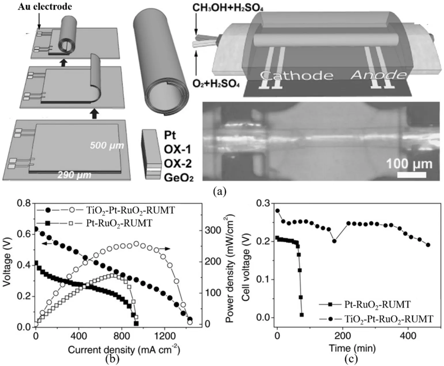
Fig.9.(a)Schematic diagram of the rolledup Pt–RuO2 microtubes(Pt–RuO2-RUMTs).fabricated with the pre-strained bilayers of RuO2 and Pt cat-NPs deposited on the sacrificial layer(GeO2).The tube was linked by two pairs of Au electrodes at the inner-and outer-wall,respectively.(b)Polarization and output power curves of theμDMFCs.(c)Transient discharging voltage-time plots of the passiveμDMFCs at the maximum power efficiency.Reprinted with permission from Ref.[123]Copyright(2017)WILEY-VCH.
Fig. 10.(a) Schematic of the singlemicrotube-device fabrication showing the planar device before rolling(left)and the device after rolling the Ge/Ti nanomembranes(middle).An optical microscopy overview image of a single rolled-up device(right).(b)Transport properties of the single Ge/Ti and Ge microtubes(left),the single Ge/Ti microtube before(red curve)and after discharging at 2 nA for 400 s(black curve)(middle),and after charging for 100 s(red curve),200 s(green curve),and 500 s(violet curve,right).Reprinted with permission from Ref.[125]Copyright(2013)WILEYVCH.(c)The schematic illustration of an encapsulated Li-ion rMB with a single silicon tube as the anode.(d)Optical microscopy image of a single rolled-up silicon microtube contacted with Ti strip lines.(e)Chemical diffusion coefficient of Li+ions in Si tube and planarfilm under various potentials during thefirst discharge.(f)Electrical conductivity at various discharge/charge states during thefirst cycle.Reprinted with permission from Ref.[126]Copyright(2014)WILEY-VCH.
5.Conclusions and perspectives
In this review,we summarized the development of 3D rMBs based on different architectures(Table 1).3D sandwiched rMBs are highly compatible with technologies that are widely used in semiconductor industries.Therefore,they can be easily integrated into on-chip electronic devices.Nevertheless,the sandwiched structure limits the thickness of electrode materials,and so does the output energy of the rMB.As a result,3D sandwiched rMBs suffer low energy density.By changing the sandwiched architecture to the interdigital architecture,the energy density can be improved thanks to the good tolerance of thick microelectrode.Moreover,3D interdigital rMBs can be fabricated on the flexible and even wearable substrates.Therefore,they hold great promise in the integration into flexible and wearable electronic devices.3D sandwiched and interdigital rMBs have governed the research of rMBs.However,they face a fatal problem for the practical applications in nextgeneration electronic devices:the large energy density relies on the large footprint area of the rMB,which opposes the rapid miniaturization of electronic devices,of which the footprint area is reduced to sub-square millimeters.To tackle this challenge,developing an advanced technology that can effectively reduce the footprint area of 3D rMBs and maintain the high energy density is of great importance.As such,the rolled-up nanotechnology that transforms 2D devices into 3D devices becomes a promising solution.Several prototype rMBs based on the rolled-up nanotechnology have been developed and shown encouraging results of high energy density and small footprint area(Table 1).Towards the accomplishment of the ideal rMBs with high output energy and minimal footprint area,the rolled-up nanotechnology should be universal for diverse battery designs and electrode materials because the energy storage ability largely depends on the inherent properties of electrochemically active materials.
Table 1 Performance comparison of rMBs with different configurations.
Besides,electrolytes for rMBs are crucial for thefinal product.Firstly,the electrolytes should provide high ionic conductivity.Based on this criterion,liquid electrolytes are appropriate.However,a liquid electrolyte poses the challenge of packaging because the leakage of the electrolyte during operation should be avoided.Solid-state electrolytes,such as LiPON,has been widely used in microbatteries.They can solve the problem of leakage but show a lowionic conductivity[127–129],which impairs the energy storage ability of rMBs.Alternatively,polymer-based electrolytes are able to reach a balance between high ionic conductivity and good stability during the operation[130].For example,the hydrogel electrolytes are optimized to show long-term water retentions,providing the high ionic conductivity for aqueous batteries over cycling.Likewise,the lithium ion microbatteries using polymer electrolytes usually show better performance than those using LiPON [35].Moreover,functional properties,for instance,self-protection[131,132],can be realized by the polymer-based electrolyte to further enhance the safety and stability of rMBs.
Last but not least,packaging issues need to be addressed to realize high-density integration of rMBs in microelectronic systems.The package of rMBs should be able to protect electrode materials,especially for metal based rMBs,[13,84,85]because the metal anodes are sensitive to moisture and oxygen.A general packaging solution is depositing a polymer shield layer on the metal anodes.Then,a second layer of ceramic or metallic material covers the polymer layer and forms a protective barrier against oxygen and moisture[64,139].For the interpenetrated electrodes embedded in the substrate,a simple way to seal the rMB is layering down a sealing layer over electrodes.
In summary,the development of rMBs for next-generation electronic devices requires the advancement of the micromachining technologies,the innovation of high-performance electrode materials that are compatible with microfabrication,and the utilization of safe and stable electrolytes.
Declaration of competing interest
None.
Acknowledgment
Funding:Y.L.,J.Q.,F.L.,Z.Q.,H.T.,and L.L.acknowledge the support and funding from China Scholarship Council(CSC).O.G.S.acknowledgesfinancial support by the Leibniz Program of the German Research Foundation(SCHM 1298/26-1).
杂志排行
Namo Materials Science的其它文章
- GUIDE FOR AUTHORS
- Editorial for a special issue“Nano energy materials and devices for miniaturized electronics and smart systems”
- Aim & Scope
- Low-power emerging memristive designs towards secure hardware systems for applications in internet of things
- A comprehensive review of miniatured wind energy harvesters
- Recent developments of stamped planar micro-supercapacitors:Materials,fabrication and perspectives