An easily-prepared impedance matched Josephson parametric amplifier∗
2021-06-26YaPengLu卢亚鹏QuanZuo左权JiaZhengPan潘佳政JunLiangJiang江俊良XingYuWei魏兴雨ZiShuoLi李子硕WenQuXu许问渠KaiXuanZhang张凯旋TingTingGuo郭婷婷ShuoWang王硕ChunHaiCao曹春海WeiWeiXu许伟伟GuoZhuSun孙国柱andPeiHengWu吴培亨
Ya-Peng Lu(卢亚鹏) Quan Zuo(左权) Jia-Zheng Pan(潘佳政) Jun-Liang Jiang(江俊良)Xing-Yu Wei(魏兴雨) Zi-Shuo Li(李子硕) Wen-Qu Xu(许问渠) Kai-Xuan Zhang(张凯旋)Ting-Ting Guo(郭婷婷) Shuo Wang(王硕) Chun-Hai Cao(曹春海)Wei-Wei Xu(许伟伟) Guo-Zhu Sun(孙国柱) and Pei-Heng Wu(吴培亨)
1Research Institute of Superconductor Electronics,School of Electronic Science and Engineering,Nanjing University,Nanjing 210093,China
2Purple Mountain Laboratories,Nanjing 211111,China
Keywords: Josephson junction,parametric amplification,impedance matching,gain and bandwidth
1. Introduction
Parametric amplifiers have become essential components in quantum information processing due to their near quantumlimited noise performance.[1–5]A nonlinear resonator including Josephson junctions, whose effective inductance can be modulated, can realize parametric amplification.[6,7]Various Josephson parametric amplification(JPA)schemes have been realized by designing different coupling structures,for example, capacitively coupling a transmission line to a coplanar waveguide cavity grounded through Josephson junctions,[8–11]directly coupling a transmission line to lumped-element circuits including Josephson junctions,[12–15]and a wireless architecture JPA using a dipole antenna.[16]However,impedance matching between the nonlinear resonator and the external transmission line is not taken into account in the above mentioned architectures. The high quality factor of the nonlinear resonator leads to the limitation of the measurement efficiency and amplifier bandwidth, while wider bandwidth and higher gain of the parametric amplifiers are required for non-demolition readout with high fidelity in superconducting qubits, microwave single-photon detection, and mechanicalelectric hybrid systems.[17–19]
To achieve a higher bandwidth, impedance transformation between the external transmission line and the nonlinear resonator is introduced in the parametric amplification architecture, which pushes the resonator to its low quality factor limit. Such design schemes of impedance matching have been studied both theoretically and experimentally.[20–26]There are mainly two kinds of engineering schemes: one is aλ/4 impedance transformer, in which the impedance is matched in a fixed frequency range;the other one is a hybrid structure impedance taper line containing coplanar waveguide (CPW)and strips, which provides impedance matching in a flexible frequency range due to the cosin-like ripple change of the imaginary part of the impedance. However, the latter architecture is relatively more complicated in the fabrication due to the requirement of higher precision in the overlay align and less defects in the fabrication process.
In this work, we present an alternative and easilyprepared impedance matched parametric amplifier(IMPA)architecture containing CPW-strip hybrid structure. Unlike the previous designs, the upper plates of capacitors in the taper transmission line and nonlinear resonator have not be connected to the lateral ground. Such design avoids making vias between the upper plate of capacitors and the reference ground. Thus the requirements for lithography alignment and precision are greatly reduced, which makes the fabrication process more reliable with easy preparation. Furthermore,the quality of the capacitor is improved leading to a broadband Josephson parametric amplifier with excellent performance.The experimental results show that the device fabricated using this design provides higher than 25 dB gain in the bandwidth of 100 MHz while maintaining the dynamic performance and noise level of the device at the same level as other similar IMPA. A bandwidth of about 400 MHz can also be obtained with a gain of about 17 dB with an optimal magnetic flux.
2. Sample and experimental setup
An optical micrograph of our IMPA is shown in Fig.1(a).It consists of an impedance taper transmission line and an LC nonlinear resonator based on a dc-SQUID containing two Josephson junctions in a supercouducting loop. A Klopfstein taper line is designed using CPW-strip hybrid structure without grounding, unit of which is shown in Fig. 1(b). As one can see, the capacitance is not only distributed between the upper plate and the center conductor of CPW, but also between the upper plate and the lateral ground. By increasing the density of the strips in gradient along the coplanar waveguide line,the impedance of the taper line varies from 50 Ω to 15 Ω smoothly. The schematic circuit diagram of the device is shown in Fig.1(c). The coplanar waveguide is formed of a center conductor of widthw=20µm separated from the lateral ground planes by a gap of widths=10 µm. The length of the CPW line is 20 mm,and the characteristic impedance is 50 Ω. The size of the strip is 80µm×5µm, which provides high fault tolerance in the fabrication of capacitors of the taper line.

Fig.1. (a)Micrograph of an IMPA.(b)Micrograph of a CPW-strip hybrid structure. (c)Equivalent circuit diagram of an IMPA.
Here is the detailed fabrication process. Firstly,a 100 nm thick niobium film is deposited on an intrinsic silicon wafer with high resistance. Then the CPW line and bottom plate of the LC capacitor are patterned with optical lithography and reactive ion etching (RIE). Secondly, a 200 nm thick silicon nitride (SiNx) film is deposited on the whole wafer using plasma-enhanced chemical vapor deposition(PECVD)to form the dielectric layer of the capacitors with high quality.Then the upper plates of all lumped capacitors are patterned and a 100 nm thick aluminum film is evaporated and lifted off to form lumped capacitors. Thirdly, all SiNxfilms except those around the upper plate and transmission line are exposed in optical lithography and etched by RIE. Till now the impedance taper line and the capacitor of the LC resonator are obtained.[27]Finally,a Dolan bridge structure is patterned by electron-beam lithography[28]and double-angle evaporation of aluminum is used to define a dc-SQUID consisting of two Josephson junctions. The loop of the dc-SQUID has an area of 20 µm×10 µm, and the size of each junction is 1.2µm×1.6µm.
The measurement system is depicted schematically in Fig.2,all measurements are performed in an Oxford dilution refrigerator system with a base temperature of 30 mK.The input line is heavily attenuated at various temperature plates to avoid thermal noise.The amplified reflected signal is routed to the output line by a cryogenic circulator at the mixing chamber stage of the cryostat. A 10 cm length cable is used to connect the IMPA and circulator. The DC magnetic flux bias line and AC pumping line of the dc-SQUID are combined by a bias-tee. To measure the reflected signal more efficiently, a cryogenic high electron mobility transistor(HEMT)amplifier with a gain of 35 dB and a noise temperature of 4 K around 7 GHz is used.The output signal is further amplified by roomtemperature amplifiers and recorded by a vector network analyzer or a signal analyzer.

Fig.2. Schematics of the measurement setup.
3. Results and discussion
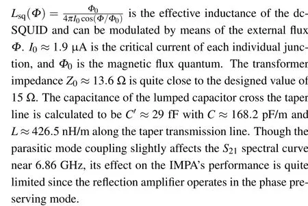
The phase of reflection coefficient of the resonator as a function of DC magnetic flux is measured using a vector network analyzer. As shown in Fig. 3, the resonant frequency can be tuned from a maximum of 7.515 GHz down to 6 GHz.Parameters are obtained by fitting the following equation:

whereCr≈7.46 pF is the capacitance of the plate capacitor.Lstray≈3.5 pH is the stray inductance in the LC circuit.
The gain and bandwidth performance of IMPA is characterized in detail by calculating the ratio of reflected power with and without the presence of pump tone. By applying a pump tone offpump=13.96 GHz through the AC magnetic flux line with DC working point ofΦDC=0.32Φ0,the IMPA works in a three-wave mixing mode.We use a signal generator to create a coherent signal with low enough incident power of−135 dBm,and record the power of the reflected signals with different pump power using a spectrum analyzer. The gain is shown in Fig.4 as a function of the signal frequency and pump power. Data at pump power ofPpump=−49.1 dBm is shown in Fig.5(a),in which we have a gain higher than 25 dB and a bandwidth larger than 100 MHz. Further increasing the pump power,such asPpump=−48.5 dBm,will reduce the gain,but the corresponding bandwidth will slightly increase. By adjusting the working point,i.e.,the DC magnetic flux bias,one may obtain better performance. For example, as shown in Fig. 6(a), whenΦDC= 0.25Φ0, withfpump= 12.761 GHz,Ppump=−42.6 dBm, a gain of higher than 17 dB can be obtained,while the bandwidth is increased to be about 400 MHz.
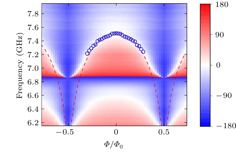
Fig. 3. Phase of reflection coefficient of the resonator as a function of DC magnetic flux. The resonance frequencies measured(blue circles)are fitted by Eq.(1)(red dashed line).

Fig. 4. Measured power gain as a function of the pump powers and the incident signal frequencies at ΦDC = 0.32Φ0. Two dashed lines refer to the profile curves plotted in Fig. 5(a) with Ppump = −49.1 dBm and Ppump=−48.5 dBm,respectively.
Fig. 5. (a) Measured gain with Ppump = −49.1 dBm and Ppump =−48.5 dBm, respectively. (b) 1 dB compression point. (c) Noise performance of the device with fpump =13.96 GHz, Ppump =−49.1 dBm, and ΦDC=0.32Φ0.

Fig. 6. (a) Measured gain and (b) noise performance of the device with fpump=12.761 GHz,Ppump=−42.6 dBm,and ΦDC=0.25Φ0.
The saturation power of an amplifier is defined as a critical value of the signal power at which the corresponding gain is decreased by 1 dB. We record repeatedly the gain with a frequency interval of 5 MHz from 6.825 GHz to 7.125 GHz with different input powers and extract the saturation powers of the IMPA.As shown in Fig.5(b),the IMPA has a saturation power of−118 dBm in a high bandwidth with 25 dB gain.Reducing the gain can effectively improve the power value of 1 dB compression point. As shown in Fig. 7, we investigate the dependence of the gain at a frequency of 6.975 GHz with different pump powers. When the gain is about 27 dB, the saturation power is found to be−120 dBm. However when the gain is about 21 dB, the saturation power increases to be−112 dBm.
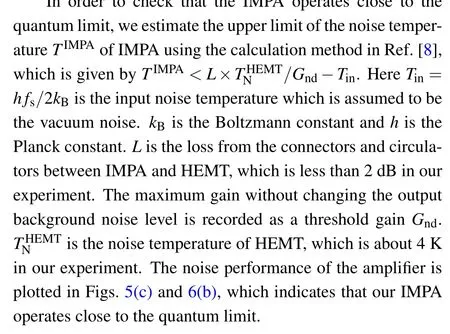
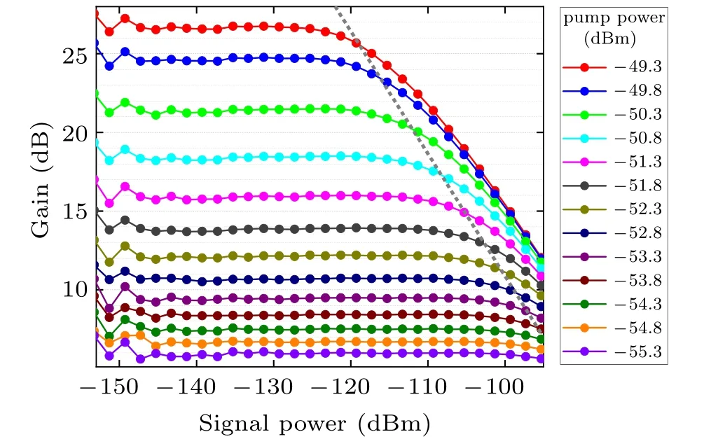
Fig. 7. Measured gain as a function of the incident signal power for fs =6.975 GHz. The dash line indicates the 1 dB compression point slope as a function of gain.
4. Conclusion
In summary,we have designed,fabricated,and characterized an impedance matched Josephson parametric amplifier,in which the impedance matched line is realized using CPWstrip hybrid structure without grounding. This new design makes the fabrication process more reliable and the requirements for lithography alignment and precision are considerably decreased. A gain higher than 25 dB with a bandwidth of about 100 MHz is obtained. By adjusting the working point,a higher bandwidth of about 400 MHz can be obtained with a gain higher than 17 dB. The noise temperature of IMPA is estimated to be close to the quantum limit. All of these results show that the Josephson parametric amplifier with this reliable and convenient design can be used as a first stage of amplification in the multi-qubits readout and/or microwave singlephoton level readout.
猜你喜欢
杂志排行

Chinese Physics B的其它文章
- Coarse-grained simulations on interactions between spectrins and phase-separated lipid bilayers∗
- Constraints on the kinetic energy of type-Ic supernova explosion from young PSR J1906+0746 in a double neutron star candidate∗
- Computational model investigating the effect of magnetic field on neural–astrocyte microcircuit∗
- Gas sensor using gold doped copper oxide nanostructured thin films as modified cladding fiber
- Exact explicit solitary wave and periodic wave solutions and their dynamical behaviors for the Schamel–Korteweg–de Vries equation∗
- Suppression of ferroresonance using passive memristor emulator