Understanding the synergistic effect of mixed solvent annealing on perovskite film formation∗
2021-06-26KunQian钱昆YuLi李渝JingnanSong宋静楠JazibAliMingZhang张明LeiZhu朱磊HongDing丁虹JunzheZhan詹俊哲andWeiFeng冯威
Kun Qian(钱昆) Yu Li(李渝) Jingnan Song(宋静楠) Jazib Ali Ming Zhang(张明) Lei Zhu(朱磊)Hong Ding(丁虹) Junzhe Zhan(詹俊哲) and Wei Feng(冯威)
1School of Physics and Astronomy and Collaborative Innovation Center of IFSA(CICIFSA),Shanghai Jiao Tong University,Shanghai 200240,China
2Department of Polymer Science and Engineering,School of Chemistry and Chemical Engineering,Shanghai Jiao Tong University,Shanghai 200240,China
3State Key Laboratory of Fluorinated Materials,Zibo 256401,China
Keywords: perovskite solar cell,solvent vapor annealing,dissolution,recrystallization
1. Introduction
Organic-inorganic halide perovskite materials refer to oxides of the chemical formulaABX3(A=CH3NH3,(NH2)2CH,Cs,B=Ge,Sn,Pb,andX=I,Br,Cl),which have been given numerous attentions in recent years due to their unique properties such as magnetism,ferroelectricity,etc.[1,2]Being the absorber layers in solar cells,the perovskite materials are particularly remarkable because of their optically high absorption,[3]superior charge transport properties,[4]and low exciton binding energy.[5,6]The power conversion efficiency(PCE)of perovskite solar cells (PSCs) was only 3.8% at the beginning of 2009,[3]whereas a PCE of 25.5% was achieved in the latest research.[7]
Nevertheless, perovskite-based devices are still confronted with critical challenges, such as detrimental grain boundaries and high densities of defect states caused by rapid and disordered crystallization of perovskite films.[8–10]These issues lead to radiationless recombination of carriers in perovskites, degrading the device performance.[11,12]A number of post-treatment methods have been proposed to control the crystallization rate of perovskite films to improve the crystal quality, eliminate the lattice defects, and eventually improve the device efficiency. For example,using solvent engineering to add DMSO into DMF solvent can slow down the crystallization rate by taking advantage of the strong force between Lewis acid-base adducts.[13,14]The antisolvent method,dropping a solvent with strong compatibility to the original one during the spin coating process and quickly removing the excess solvent by centrifugal force, is commonly used for controlling the crystallization rate.[15,16]Solvent vapor annealing(SVA),first proposed by Yanget al.in polymer solar cells,[17]has been proven to effectively improve device performance with excellent controllability in annealing temperature, annealing time,vapor pressure,etc.[18]
As a common post-treatment method, SVA introduces solvent molecules into the atmosphere of traditional thermal annealing. The solvent molecules preferentially reach the areas with higher surface energies,such as grain boundaries. At grain boundaries, solvent molecules enter the cubic octahedral structure of perovskite, seize organic molecules, and reform the intermediate phase in the perovskite crystallization process. At a certain temperature,the entry and volatilization of the solvent molecules reach a thermal equilibrium, where the intermediate phase is formed,leading to fusion of adjacent grains, expansion of the size of grains, and reduction of the density of defect states.[19–21]
The typical solvents used in SVA are the ones commonly used in the perovskite precursor solution.[19]However, in the past,most researches have focused on single-component SVA while solvent annealing adopting different solvents showed huge differences. For instance, DMSO has obvious advantages in expanding the grain size in SVA.However,due to its high boiling point[22]and the strong interaction between solvent molecules and perovskite components,the thermal equilibrium mentioned above can be easily broken,and perovskite films can be dissolved overly.It is also possible to form an irreversible poly-plumbate structure over a long period of time.[23]In contrast, the boiling point of DMF is lower, and the interaction force between DMF and perovskite is smaller. In this case, the thermal equilibrium is established rapidly, and the DMF molecules quickly volatilize, leaving a very short time for their interaction, so the grain fusion becomes very limited.[13]
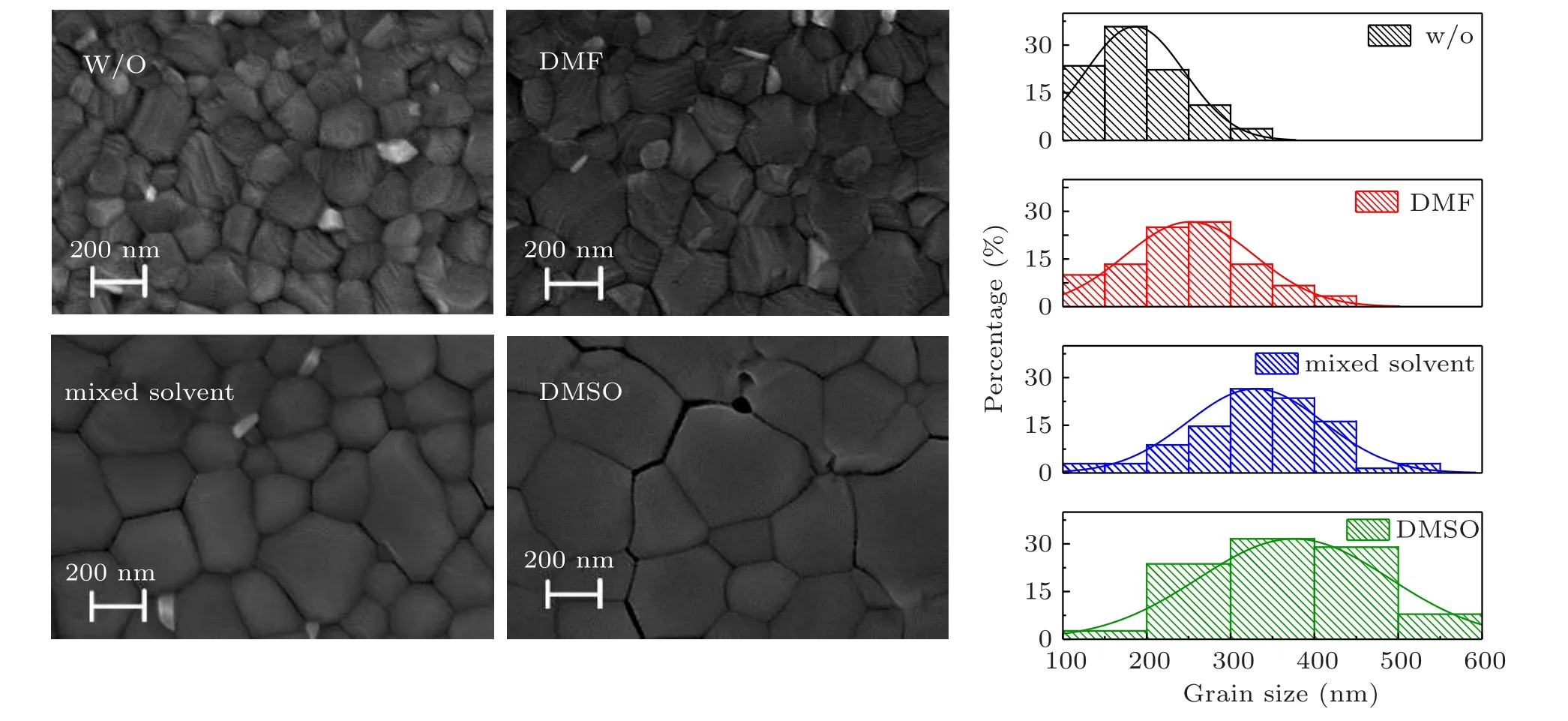
Fig.1. Top-view SEM image and the corresponding grain size distribution of perovskite film processed without and with solvent annealing treatment.
In this manuscript, DMF/DMSO mixed solvent (MS) in SVA was proposed while the effect was compared with singlecomponent SVA.The detailed process and mechanism of SVA were also described to prove the effectiveness. The MS SVA combined the advantages of the two solvents, effectively expanding the grain size and reducing the density of defect states without damaging the film. The detailed crystallization dynamics during SVA,which is of critical importance in understanding the perovskite mesophase and the transformation between mesophase and perovskite crystal,was summarized. A champion power-conversion efficiency (PCE) of 19.76% under air mass global (AM 1.5G) spectrum illumination was achieved without any doping and interface optimization compared with 17.13%of the SVA-free control device.
2. Results and discussion
Figure 1 shows the top-view SEM images of the perovskite films and their corresponding grain size distribution.The images indicate that SVA treatment increased the grain size of perovskite films regardless of the type of solvent vapor.DMSO vapor treated perovskite film exhibited the largest average grain size of∼380 nm along with clear voids and breaks between grains,which are detrimental for device performance.In contrast to DMSO treatment, the MS SVA resulted in a more uniform and compact perovskite film with an average grain size of∼330 nm.
Figure S1 shows the UV-vis absorption spectra of perovskite films based on SVA with different solvents.The nearly identical absorption spectra indicate that SVA treatment had no influence on light absorption. Further, to investigate the effect of SVA treatment on carrier recombination, we conducted the steady-state photoluminescence (PL) spectra and time-resolved PL spectra (TRPL) of bare perovskite films,with results shown in Figs.2(a)and 2(b). The highest PL intensity was observed in MS treated perovskite films,indicating non-radiative recombination was significantly suppressed. By fitting the TRPL spectra with a bi-exponential function, the carrier lifetime was extracted(Table S1)with 14.64 ns for the control device and 23.05 ns for the MS treated device. The prolonged carrier lifetime for the MS treated device indicates SVA treatment effectively passivated the defects by reducing the grain boundaries.[24,25]As for pure DMSO treated film,the carrier lifetime was largely shortened with an averageτof only 3.58 ns, meaning that the structure of perovskite film was damaged under the effect of DMSO vapor. In order to quantify the defect density, we performed space charge limited current(SCLC)measurements based on electron-only devices(ITO/SnO2/MAPbI3/PCBM/Al). As shown in Fig.2(c),there are three regions in the SCLC curves. In the first region,the applied voltage is lower than the kink point voltage,and the current increases linearly with applied voltage. When the applied voltage exceeds the kink point voltage,where the second region is, the current increases nonlinearly, indicating that all trap states are filled by the injected carriers. At higher bias, the current shows a quadratic dependence (the third region), and the dark current is well fitted by the Mott–Gurney law.Hence the intersection of the first and second region is the kink point voltage, which is also called trap-filled limit voltageVTFL,and the trap densityNtrapis calculated by using the following formula:[26,27]
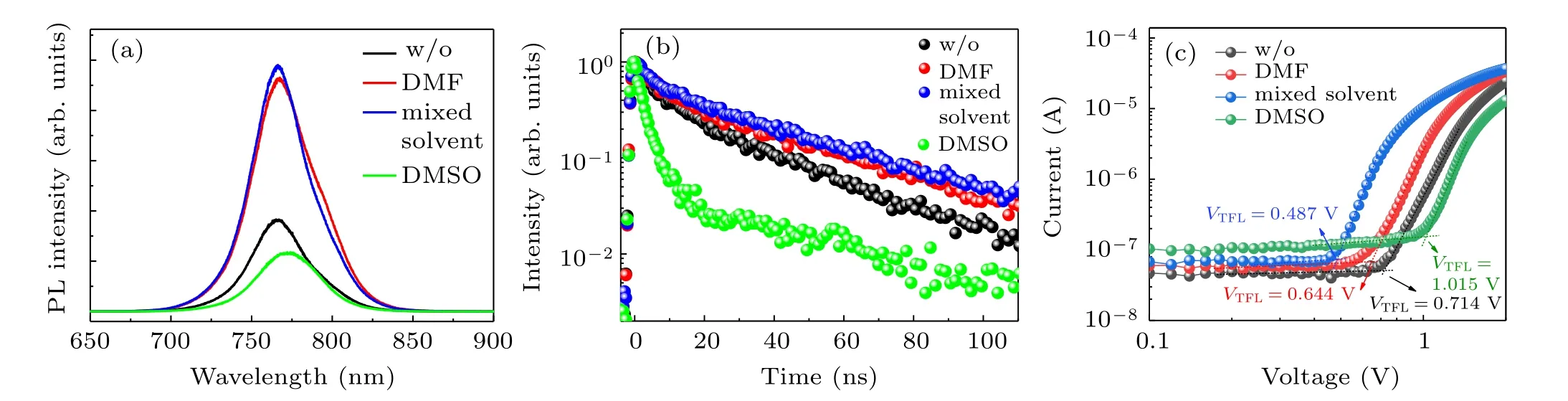
Fig. 2. (a) The PL spectra, and (b) time-resolved PL spectra of bare perovskite films processed with SVA treatment exposed to different solvent vapor.(c) Space charge limited current (SCLC) of electron-only devices with a device structure of ITO/SnO2 (40 nm)/MAPbI3 (∼340 nm)/PCBM (80 nm)/A1(100 nm). The volumes of four solvents were optimized, which is 60µL for DMF solvent, 20µL for DMF/DMSO mixted solvent and 20µL for DMSO solvent,respectively.
whereLis the thickness of the perovskite film which is around 350 nm,ε(∼18) is the relative dielectric constant of perovskite.[28]The devices after SVA with DMF and MS had lowerNtrapof 1.04×1016cm−3and 7.91×1015cm−3respectively, compared to that of 1.16×1016cm−3for the control one and 1.65×1016cm−3for the case of DMSO SVA. The reduction in defect states agrees with suppressed carrier recombination,corresponding to the significant improvement ofVOCand FF shown in Table S2.
To relate the above results with the crystallization process, we conducted the grazing incidence wide-angle x-ray scattering experiments(GIWAXS).The 2D GIWAXS images for the studied films are shown in Fig.S3,and the corresponding 1D GIWAXS profiles are displayed in Fig. 3(a). In comparison with the control device,both DMF and MS SVA processed perovskite films exhibited an improved crystallization,with the latter showing the greatest improvement. While for the DMSO case, the characteristic peak intensity of the perovskite phase was subjected to an obvious decrease. In addition, new peaks occurred atq <1.0 A−1, which could be attributed to the characteristic scattering peak of intermediate phase MAI-PbI2-DMSO.[29,30]The fitting results of the perovskite phase atq= 1.0 A−1, including the peak area and crystal size, are shown in Fig. 3(b). MS treated perovskite film showed enhanced peak area and enlarged crystal size.The results suggest that proper selection of solvent and solvent volume for SVA treatment could simultaneously enhance the crystallinity and crystal size by recrystallizing the perovskite crystals.
In light of the experimental results above,Scheme 1 was constructed to illustrate the crystallization kinetics of perovskite crystals under SVA treatment,which is made up of two processes: perovskite dissolution and recrystallization. Here we take MS SVA as an example.When the perovskite films are exposed to the MS vapor,the solvent molecules will preferentially dissolve the grain boundaries due to its high instability,and then form an intermediate phase of MAI-PbI2-DMF and MAI-PbI2-DMSO,[23]which refers to the process of dissolution. However, with thermal annealing treatment, the solvent molecules are extracted from the intermediate state, leading to recrystallization of the perovskite phase. In the whole process,there is a competition between dissolution and recrystallization, and the equilibrium state is dependent on the donor number[31]of solvent,boiling point,and heating temperature.Because of the small number of donors, the weak coordination between Pb2+and DMF enables easy transformation from the intermediate phase to the perovskite phase. In contrast,Pb2+and DMSO interact more strongly,demanding more energy to break the bond. By exposing the perovskite films to a proper amount of MS vapor, the balance of perovskite dissolution and recrystallization can be readily achieved,obtaining high-quality perovskite film without byproducts, as shown in the 2D GIWAXS patterns in Fig. S3. If the film exposes to excess DMSO solvent vapor, the equilibrium will be broken,and an excess amount of MAI-PbI2-DMSO will be formed,thus increasing the activation energy for phase transition and finally resulting in a poor film with byproducts, evidenced by the appearance of new scattering peaks atq <1.0 A−1(Fig.S4).
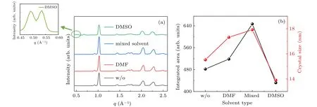
Fig.3. (a)1D GIWAXS profiles of perovskite films processed under different SVA conditions,which were derived from the 2D GIWAXS patterns by circular integration. (b)The evolution of peak area and crystal size of perovksite phase at q=1.0 ˚A−1 as a function of solvent vapor types.
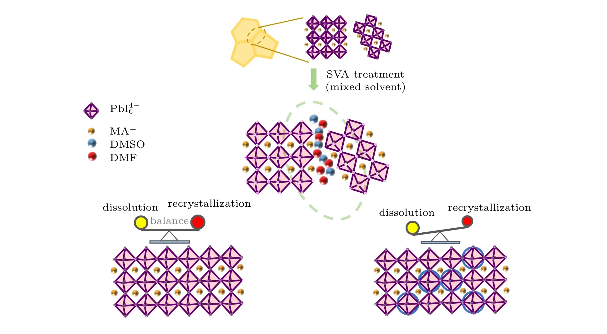
Scheme 1. Schematic diagrams illustrating the dissolution and recrystallization process of perovskite crystals under SVA treatment.
To verify the impact of SVA treatment on the resulting photovoltaic performance, we fabricated inverted-planar perovskite solar cells with the device structure shown in Fig.4(a)(ITO/PTAA/MAPbI3/PCBM/Al). Figure 4(b) shows the best photocurrent density–voltage (J–V) curves of perovskite solar cells under each optimized condition without and with SVA treatment, and the corresponding device parameters are summarized in Table S2. The detailed device optimization process is shown in Fig. S2. After SVA treatment, the device efficiency was improved due to the improved film quality and crystallinity as demonstrated. It can be noted that the MS treated perovskite solar cells achieved a champion efficiency of 19.76%,with improved open-circuit current(VOC)of 1.103 V,short-circuit current density(JSC)of 21.93 mA/cm2,and fill factor (FF) of 81.72%. In addition, SVA treatment eliminated theJ–Vhysteresis(Fig.4(c)).[32,33]External quantum efficiency(EQE)measurements were conducted,with results shown in Fig.4(d). It was confirmed that the integrated current density from EQE was consistent with theJSCderived from theJ–Vcurves with a deviation of 0.36 mA/cm2. Further, we checked the stable-state photocurrent and PCE output, measured at a maximum power point (0.88 V for the control device and 0.91 V for MS SVA treated devices), as shown in Fig. 4(e). The steady-state output PCE increased from 17.03% to 19.88% after SVA treatment. The device reproducibility was assessed by fabricating more than 100 cells for devices without and with MS treatment(Fig.4(f)). The average PCE for the control and MS treated devices were 16.53%and 19.37%,respectively.

Fig. 4. (a) Device structure of perovskite solar cells in this work. (b) The best photocurrent density versus voltage (J–V) curves of perovskite solar cells processed under different solvent vapor environment. (c) J–V curves of champion device scanned from both the reverse and forward directions. (d) External quantum efficiency (EQE) and integrated short current density (JSC) of control and DMF/DMSO mixed solvent treated perovksite solar cells. (e)Stable output of current density and PCE as a function of time,which were held at a maximum power point(0.88 V for the control device,and 0.91 V for mixed DMF/DMSO).(f)The PCE histograms of devices without and with mixed DMF/DMSO treatment.
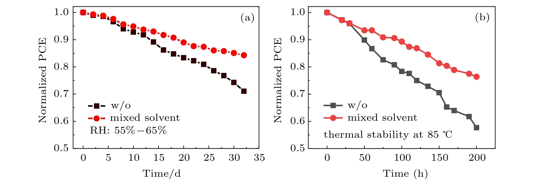
Fig. 5. (a) Normalized PCEs of unencapsulated devices exposed to ambient conditions with humidity of 55%–65%. (b) Normalized PCEs of unencapsulated devices under 85 ◦C heat treatment in a nitrogen atmosphere.
Additionally, we carried out a series of stability testing to evaluate the effect of SVA treatment on the device stability, the results of which are displayed in Fig. 5. First, the humidity stability of devices was tested by leaving the nonencapsulated devices in ambient air with a humidity of 55%–65% for 30 days. As shown in Fig. 5(a), the control device degraded to∼70% of its initial value after 30 days of tracking. In comparison, the MS SVA treated devices retained∼85% efficiency, unambiguously demonstrating improved humidity stability. Then,the thermal stability of unsealed devices was monitored by continuous annealing the devices at 85◦C under a nitrogen atmosphere for 200 h(Fig.5(b)). The MS treated device exhibited superior thermal stability, which maintained∼76% of its initial PCE after continuous annealing for 200 h. Under the same condition, the control device dropped to∼56%of its initial PCE.The above results demonstrate that SVA treatment can not only promote photovoltaic performance but also improve operational stability. Such improvement is attributed to the enlarged grain size and reduced grain boundaries, which are reported to be vulnerable when exposed to a harsh environment.[34]
3. Conclusion and perspectives
In summary,SVA was performed with mixed solvents to study its synergistic effect on the intermediate phase and crystallization of perovskite film formation. The solvent vapor acted uniformly on the surface of the film; however, excess solvent led to the dissolution of perovskite films. We proposed a model based on the GIWAXS, revealing that solvent molecules enter the grain boundaries and induce two competing processes, dissolution and crystallization, which reach an equilibrium depending on solvent type and volume. Consequently, from the overall perspective, MS SVA promoted the growth of grains and enlarged the grain size, suppressing radiationless recombination loss. With MS SVA, theVOCand FF of the completed device were improved due to significantly reduced defect states in perovskite material, and the PCE reached 19.76% compared to 17.13% of the control device. Meanwhile,both thermal stability and humidity stability were improved significantly.
猜你喜欢
杂志排行

Chinese Physics B的其它文章
- Coarse-grained simulations on interactions between spectrins and phase-separated lipid bilayers∗
- Constraints on the kinetic energy of type-Ic supernova explosion from young PSR J1906+0746 in a double neutron star candidate∗
- Computational model investigating the effect of magnetic field on neural–astrocyte microcircuit∗
- Gas sensor using gold doped copper oxide nanostructured thin films as modified cladding fiber
- Exact explicit solitary wave and periodic wave solutions and their dynamical behaviors for the Schamel–Korteweg–de Vries equation∗
- Suppression of ferroresonance using passive memristor emulator