In-plane oriented CH3NH3PbI3 nanowire suppression of the interface electron transfer to PCBM∗
2021-06-26TaoWang王涛ZhaoHuiYu于朝辉HaoHuang黄昊WeiGuangKong孔伟光WeiDang党伟andXiaoHuiZhao赵晓辉
Tao Wang(王涛), Zhao-Hui Yu(于朝辉), Hao Huang(黄昊),Wei-Guang Kong(孔伟光), Wei Dang(党伟), and Xiao-Hui Zhao(赵晓辉)
Hebei Key Laboratory of Optic-Electronic Information Materials,College of Physics Science and Technology,Hebei University,Baoding 071002,China
Keywords: lead-halide perovskite,nanowire,interface electron transfer,transient absorption spectroscopy
1. Introduction
Perovskite solar cells (PSCs) belong to a new generation of solar cells, whose champion power conversion efficiency(PCE)has reached to 25.2%.[1]The perovskite film has also shown excellent performance in the field of photoelectrical detector, light-emitting diode, and x-ray detector.[2–6]In these applications, improving the interface charge separation efficiency is of great importance.[7,8]So far, various strategies such as hot casting, solvent annealing, mixed solvents technique, anti-solvent dripping, and the interface engineering have been developed for optimizing the perovskite film morphology.[9–12]Compared to compact perovskite film (CPVK),nanowire perovskite film(N-PVK)exhibits significant advantages, such as superior anti-reflection, significant light trapping, and enhanced carrier transport, which are all beneficial for applications in opto-electronics.[13,14]N-MAPbI3films were first employed by Forroet al. in the field of lightemitting transistors.[15]The first N-MAPbI3-based solar cell shows a more efficient interface transfer efficiency than that of typical C-PVK film and provides a 14.17%PCE.[16]Later on, N-PVK was more used in photodetector for its better oriented carrier transport.[17–20]Only a few of investigations of N-PVK-based solar cells have been performed. One report by Kilwon Choet al.claimed that the fine control of the morphology of N-MAPbI3(diameter,surface coverage,distribution at surface or bulk)is required for optimum N-MAPbI3-based solar cells.[21]Another research pointed out that the N-MAPbI3film has a lower interface charge transfer efficiency than that of nanocube and nanowire hybrid film.[14]The above two references stressed that more gaps and holes in N-PVK lead to loose contact between N-PVK and the charge transport materials,which results in lower PCE.However,to the best of our knowledge, there are few relevant dynamic experiments for such a judgement. In consideration of widely use of N-PVK in solar cells and photodetectors, its interface charge transfer dynamics deserves a more detailed investigation.
In this paper,interface electron transfer dynamics from CMAPbI3film, as well as in-plane oriented N-MAPbI3film to PCBM were studied by using femtosecond transient absorption spectroscopy. The target carrier recombination dynamics were extracted from probe wavelength where the induced refractive change can hardly affect the transmitted light intensity. An efficient interface charge transfer phenomenon between C-MAPbI3film and PCBM was demonstrated in ours experimental results. While efficient interface electron transfer was absent from N-MAPbI3/PCBM interface, no matter of carrier generation density or observation time scales from some picosecond to tens nanosecond. Hot electron transfer at C-MAPbI3/PCBM interface was detected in excitation density varying experiment. The hot electron transfer accelerates the decay of carrier concentration of C-MAPbI3in first 10 ps–20 ps.
2. Experimental section
2.1. Materials
Methylammonium iodide (MAI, purity>99.99%) and lead (II) iodide (PbI2, purity>99.99%) were bought from Xi’an Polymer Light Technology Corp. Isopropanol(IPA,purity>99.8%),toluene(AR),N,N-Dimethylformamide(DMF,purity>99.8%, Sigma), 1-Methyl-2-pyrrolidone (NMP, purity>99.5%, Sigma) Chlorobenzene (CB, purity>99.99%,Kermel) are all kept in a N2-filled glovebox before use. The indium tin oxide(ITO)glasses were bought from South China Xiang Science&Technology Company Limited.
The ITO glass substrates were first cleaned with detergent,then were successively washed with deionized water,isopropanol,deionized water,acetone,and isopropanol in an ultrasonication bath at 30◦C for 20 min,and finally were dried with nitrogen flow.After treated with oxygen plasma(30 min),the substrates were transferred to a N2-filled glovebox for further use.
2.2. Compact MAPbI333 film
The 1-ml MAPbI3precursor solution was prepared by dissolving 580-mg PbI2and 200-mg MAI in the mixed solvent of 600-µL DMF and 400-µL NMP,and then was stirred overnight at 30◦C.35µL of MAPbI3solution was spin-coated on the substrate at 1000 rpm for 8 s and 4000 rpm for 12 s.At the 4th second before the end 75 µL of toluene solution was dipped to achieve a smooth surface. And the as-prepared MAPbI3film was kept alone for 30 min,then it was annealed at 90◦C for 9 min. The average thickness of C-MAPbI3is about 400 nm.
2.3. Nanowire MAPbI333 film
The 1-ml PbI2solution was prepared by dissolving 462-mg PbI2in 1-mL DMF, and then it was stirred over night at 30◦C for use. The 1-ml MAI solution was prepared by dissolving 10-mg MAI in mixed solution of 1000-µL isopropanol and 50-µL DMF,and also it was stirred overnight at 30◦C for use. The 30 µL of PbI2solution of 70◦C was spin-coated on the prepared substrate at 3000 rpm for 5 s and 6000 rpm for 5 s. After kept alone for 10 min the as-prepared PbI2film was annealed at 70◦C for 3 min, then it was cooled down to room temperature. The 70µL of MAI solution was loaded on the PbI2and kept alone for 4 s,then it was spun at 1500 rpm for 20 s and kept alone 15 min till the color of as-prepared film completely turned to dark-brown from light-brown, then annealed at 100◦C for 5 min. The average thickness of NMAPbI3is about 300 nm.
2.4. PCBM treatment film
PCBM solution was prepared by dissolving 20 mg of PCBM in 1 mL of chlorobenzene. When the perovskite film was cooled down from annealing for 5 min, the as-prepared PCBM solutions were dripped onto the perovskite layer,then the film was spun at a speed of 1500 rpm for 30 s.
2.5. Characterizations
The ultraviolet-visible (UV-vis) absorption spectra were recorded by UV-2600 (Shimazu). Scanning electron microscope (SEM) images were obtained by Zeiss Sigma at a 3.0-kV accelerating voltage. The surface morphology was measured by atomic force microscopy (AFM, Multimode 8,Bruker). The thickness of the film was measured by a step profiler (Dektak-XT Bruker). The x-ray diffraction (XRD)patterns were measured by a D/max 2400 x-ray diffractometer with Cu Kαradiation (λ=1.54050 ˚A). The photoluminescence (PL) measurement uses a CW laser (532 nm) as excitation source and the emission from perovskite film was recorded by a liquid nitrogen cooled CCD detector array attached to an Acton SP 2500 spectrometer. Time-resolved photoluminescence(TRPL)was recorded by a frequency-domain fluorometry with excitation wavelength at 405 nm.
2.6. Transient absorption spectrum measurement
Femtosecond transient absorption spectra measurements were conducted using a femtosecond laser (Spirtfire ACE 100F 800 nm, full width at half maximum (FWHM) pulse width 100 fs, 1-kHz repetition rate) and an ultrafast spectroscopic system(Harpia). The output of fundamental laser was split into pump (95%) and probe (5%) beams. The pump beam was directed through an optical parametric amplification system (TOPAS Prime-F) to generate 550-nm pump beam,while the probe beam was passed through an optical delay rail and focused onto a Ti:sapphire crystal to generate a white light continuum. The angle between polarization directions of pump beam and probe beam was set up as magic angle 54.7◦and the optical delay stage provided a probe time window of 8 ns.
3. Results and discussion
The surface morphologies of both types of MAPbI3film are shown in Fig. 1. As shown in Fig. 1(a), the surface of N-MAPbI3is uniformly covered by nanowires. Its extended view in the inset shows that most of N-MAPbI3nanowires are in-plane-oriented and amount of gaps and holes exists between them.The C-MAPbI3is in poly-crystal form,which looks like MAPbI3riprap(Fig.1(b)). The diameter of grain crystal is in the order of hundreds of nanometers. According to AFM measurement, the roughnessRqof C-MAPbI3is 3.76 nm, much smaller thanRq57.2 nm of N-MAPbI3.
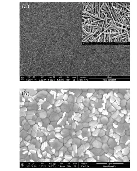
Fig. 1. SEM images of N-MAPbI3 (a) and C-MAPbI3 (b), the inset in panel(a)shows an extend view of N-MAPbI3.
The XRD patterns of C-MAPbI3and N-MAPbI3are shown in Fig. 2. The patterns of both C-MAPbI3and NMAPbI3contain diffraction plane (110) and (220) peaks at 14.2◦and 28.7◦, which indicate preferential tetragonal structure. Other noticeable differences in N-MAPbI3with respect to C-MAPbI3includes a weaker(220)peak and stronger(112),(211), (202), and (310) peaks, indicating different morphologies between them. It is should be noted that the XRD peak at 12.6◦in N-MAPbI3originates from residual PbI2,because the amount of MAI was limited in preparation of N-MAPbI3by two-step method. The residual PbI2mainly locates near the substrate and does not affect interface charge transfer from N-MAPbI3to PCBM.
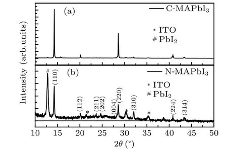
Fig.2. XRD patterns of C-MAPbI3 (a)and N-MAPbI3 (b).
Steady absorption spectra of C-MAPbI3,N-MAPbI3,and their counterparts covered by PCBM are shown in Fig.3.Both exciton absorptions of C-MAPbI3and N-MAPbI3films locate at about 750 nm.[22]A remarkable absorbance from 750 nm to 800 nm in N-MAPbI3film was attributed to surface scattering,not sub-bandgap absorption.[23]This attribution is in consistent with similar PL spectra of C-MAPbI3and N-MAPbI3(Fig. 3). The PCBM coating does not affect steady PL of CMAPbI3film,but leads a little blue shift of PL of N-MAPbI3(Fig. S1). It is consistent with the reported passivation effect of PCBM on trap states in MAPbI3.[24]
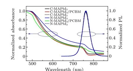
Fig. 3. Steady absorption spectra of C-MAPbI3 (black solid line),C-MAPbI3/PCBM (red solid line), N-MAPbI3 (blue solid line), NMAPbI3/PCBM(green solid line),and steady PL of C-MAPbI3 (black dash line),N-MAPbI3 (blue dash line).
To observe charge recombination in MAPbI3and electron transfer to PCBM at its interface, transient absorption spectroscopy is a powerful tool. Typical transient absorption spectra at some time delays for C-MAPbI3and N-MAPbI3are presented in Figs.4(a)and 4(c). Both transient absorption spectra of C-MAPbI3and N-MAPbI3show similar features, with a ground state bleach (GSB) signal centered at 760 nm and a broad photo-induced absorption(PIA)signal around 600 nm.Within the first 1 ps, isosbestic point of their transient absorption spectra appears blue shifts first, then red shifts successively due to hot carrier cooling.[25]Transient absorption spectra of C-MAPbI3/PCBM and N-MAPbI3/PCBM have also been presented in Fig.S2. They have similar spectral features with their counterparts without PCBM covering in our monitoring wavelength range.
We compared kinetics of absorbance change(∆mOD)for C-MAPbI3film, N-MAPbI3film, and their counterparts with PCBM covering. Monitoring wavelengths were selected at 601 nm (PIA) and 761 nm (GSB). PCBM has a small absorbance at 550 nm(Fig.S3),and its transient absorption signals at 601 nm and 761 nm are much smaller with respect to that of MAPbI3(Fig.S4). Therefore,the absorbance changes(∆mOD) of four types films at 601 nm and 761 nm are only related to the charge carrier concentration in MAPbI3. The kinetic traces of C-MAPbI3and N-MAPbI3were compared in Fig.S5 in the Supplementary materials. N-MAPbI3film displays more faster decay in kinetics traces at the 601 nm(PIA)and 760 nm (GSB), indicating a shorter carrier lifetime than that of C-MAPbI3film. The comparison of kinetic traces of C-MAPbI3and C-MAPbI3/PCBM are presented in Fig.4(b).Obviously,C-MAPbI3/PCBM kinetics traces at 601 nm(PIA)and 760 nm(GSB)show much faster decays. This is the evidence of interface electron transfer from C-MAPbI3to PCBM,which reduces the carrier lifetime of MAPbI3. But the faster decay of absorbance change (∆mOD) of C-MAPbI3/PCBM is only sustained for about 20 ps according to Fig. 4(b) and Fig. S6. It means electron transfer rate decreases with time.The mechanism of this fast electron transfer process would be explained later.
In contrast to C-MAPbI3, the kinetics of absorbance change (∆mOD) of N-MAPbI3/PCBM was nearly overlaid with that of N-MAPbI3film at first 20-ps time scale(Fig.4(d))and nanosecond scale(Fig.S7). It seems that electron transfer at N-MAPbI3/PCBM interface is less efficient than that of CMAPbI3/PCBM.
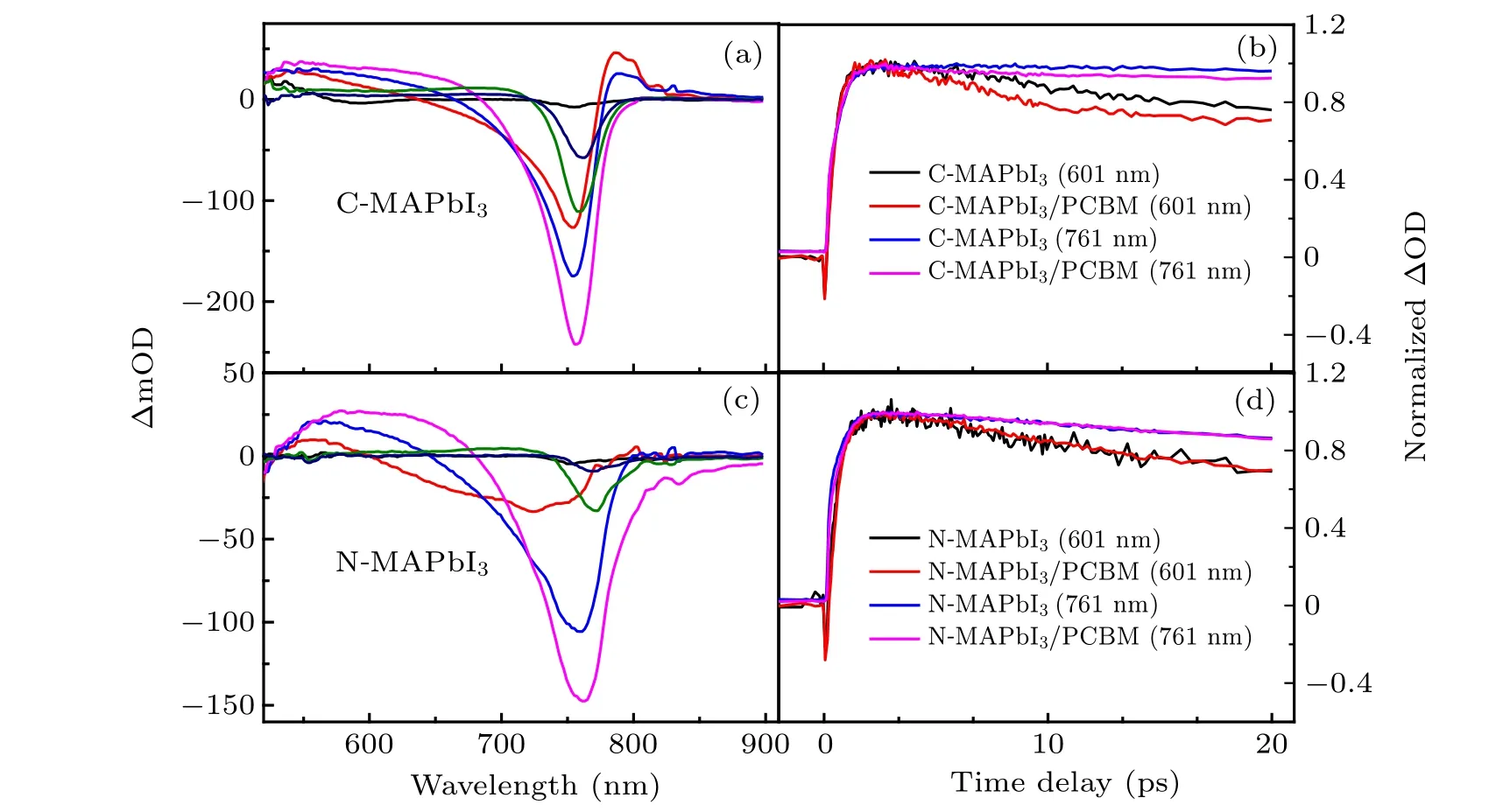
Fig. 4. Panels (a) and (c) are differential transmission spectra (mOD) for C-MAPbI3 and N-MAPbI3 films after excitation at 550 nm (1 kHz, 100 fs,155µJ/cm2): black(0 ps),red(0.3 ps),blue(0.6 ps),magenta(1.24 ps),olive(919.95 ps),and navy(4049.95 ps). Panels(b)and(d)are normalized photo-induced absorption kinetics(601 nm)and negative bleaching kinetics(761 nm)of C-MAPbI3 and N-MAPbI3 films.
We also checked the electron transfer process at CMAPbI3/PCBM interface and N-MAPbI3/PCBM interface at hundreds of nanoseconds time scales by use of TRPL technique, as shown in Fig. 5. All TRPL decay curves were fitted by multiple exponential decay function. Detailed fitting parameters are shown in Table S1. The PL lifetime of the CMAPbI3film is 128.5 ns,and it decreases to 20.68 ns as being covered by PCBM.By contrast,the PL lifetime of N-MAPbI3is 10.62 ns that is very close to the PL lifetime (9.26 ns) for N-MAPbI3/PCBM. TRPL measurements also confirm a less efficient electron transfer at N-MAPbI3/PCBM interface than that of C-MAPbI3/PCBM interface. At MAPbI3/PCBM interface, carrier transfer process is coexisted and competes with carrier recombination in MAPbI3. We attribute more efficient electron transfers at C-MAPbI3/PCBM interface to close contact between C-MAPbI3and PCBM and longer carrier lifetime in C-MAPbI3(Fig. S5 and Fig. 5). While N-MAPbI3shows loose contact with PCBM and shorter carrier lifetime,both of which are disadvantages for the interface electron transfer. In addition,MAPbI3nano-wire inherits a better diffusion coefficient than that of MAPbI3film.[26]Thus carriers in in-planeoriented N-MAPbI3diffuse along radial direction more faster than that of C-MAPbI3, lowering the carrier concentration at the interface. We suppose it as another disadvantage for NMAPbI3nanowire investigated in this research.
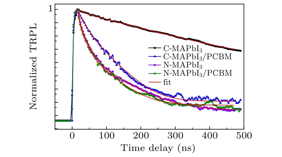
Fig. 5. TRPL decay curves of C-MAPbI3 (black line and square), CMAPbI3/PCBM(blue line and triangle),N-MAPbI3 (purple line and diamond),and N-MAPbI3/PCBM(green line and triangle)and their fitting(red line).
The interface charge transfer between MAPbI3and electron transfer material or hole transfer material undergoes a competition with charge trapping and recombination within MAPbI3. It has been reported that interface charge transfer effciiency is highly dependent on the excitation density.[27,28]In lighting this,here we also checked the effect of carrier concentration on the charge transfer between C-MAPbI3and PCBM.Kinetics at 601 nm(PIA)was chosen for such analyzation for its shorter rising phase in time than that of 761 nm (GSB)(Fig. S5) and less interference with transient reflectivity than that of 761nm(GSB)(Fig.S8).
All kinetics at 601 nm (PIA) of C-MAPbI3and CMAPbI3/PCBM under three different excitation densities were fitted with the convolution of Gaussian function and three exponential decays function, as shown Figs. 6(a)–6(c). Fitting parameters of three time components are shown in Table 1 and their standard errors are supplied in Table S1. Three features can be observed from fitting results in Table 2. Firstly, the addition of PCBM induces a reduction in all time constants when a low excitation density of 70µJ/cm2is used. Secondly,at medium excitation density of 155 µJ/cm2, the addition of PCBM only induces a reduction in the fastest time component (10 ps–20 ps). Thirdly, the addition of PCBM does not change the time constants obviously as the excitation density is as high as 284µJ/cm2. According to reduction of average carrier lifetime of C-MAPbI3in Table 1,higher electron transfer efficiency to PCBM occurs with low and medium excitation density.
In our transient absorption measurement(see Figs.6(a)–6(c)),the photo-generate carrier density is estimated as 1.0×1018cm−3, 2.2×1018cm−3, and 4.0×1018cm−3, respectively(using reflectivityR=0.17,absorbance coefficientα=105cm−1, pump beam focus diameter 300 µm). It has been reported that Auger recombination becomes dominant at very high carrier density (≥2×1018cm−3–5×1018cm−3),[29,30]which is consistent with our experimental results in Fig. S9,The electron transfer from C-MAPbI3to PCBM we measured competes with Auger recombination and bi-molecule recombination. Higher carrier density accelerates carrier high order recombination within the MAPbI3,leading the decrease of electron transfer efficiency.
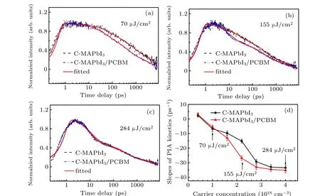
Fig. 6. Comparisons of photo-induced absorption kinetics (601 nm) for C-MAPbI3 and C-MAPbI3/PCBM under three excitation densities and their fittings[(a)–(c)],and dependence of slopes of kinetics(601 nm)for C-MAPbI3 and C-MAPbI3/PCBM in the first 10 ps–20 ps.
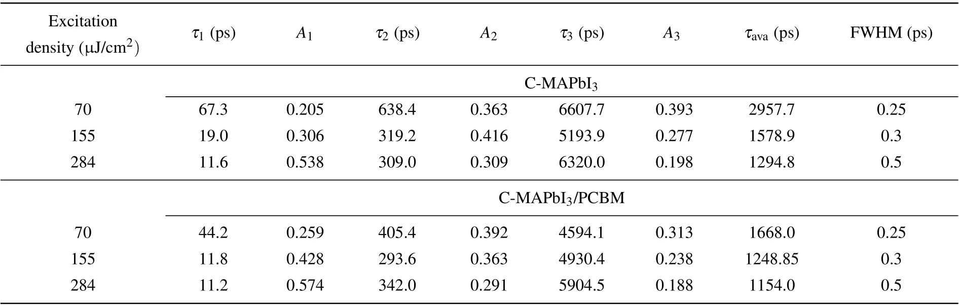
Table 1. Time components for C-MAPbI3 and C-MAPbI3/PCBM following multiple exponential decay fitting. Note that the carrier density affects the rising phase of kinetics of PIA at 601 nm,so different full width and half magnitudes(FWHM)of Gaussian function were used.
The electron transfer time can be estimated as the difference of the reciprocal of carrier density decay lifetime with and without PCBM covering,[31]as shown in the formula
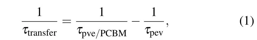
whereτpevis the decay lifetime of the carrier in CMAPbI3,τpve/PCBMis the decay lifetime of the carrier in CMAPbI3/PCBM,τtransferis the electron transfer lifetime. Under the excitation density of 70µJ/cm2, carrier concentration decay in C-MAPbI3was fitted well by use of three components with decay lifetime of 67.3 ps (44.2 ps), 683.4 ps(405.4 ps),and 6607.7 ps (4594.1 ps), respectively. These decay lifetimes indicate decay rates of carrier concentration at different time delays after photo excitation, and were determined by the residual carrier concentration in C-MAPbI3. According to these decay lifetimes and formula(1),the electron transfer lifetimes between C-MAPbI3and PCBM interface were estimated as 128.8 ps, 997.0 ps, and 1.5×10⁴ps, which respectively corresponds to the three stages of carrier recombination process. Obviously, the electron transfer lifetime between CMAPbI3and PCBM increases with carrier concentration decrease. As the carrier concentration decreases to the level that used in our TRPL measurement,the electron transfer time increases to 24.6×10⁴ps.
Finally we focus on the faster electron transfer between C-MAPbI3/PCBM interface under excitation density of 155µJ/cm2(see Figs.4(b)and 6),where carrier concentration decay lifetime of C-MAPbI3reduces from 19.0 ps to 11.8 ps(see Table 1)with covering by PCBM.Correspondingly, carrier concentration decay lifetime of C-MAPbI3under excitation density of 70µJ/cm2reduces from 67.3 ps to 44.2 ps(see Table 1). By use of formula (1), the electron transfer lifetimeτtransferbetween C-MAPbI3and PCBM in the first tens picosecond time scale is 31.8 ps under excitation density of 155µJ/cm2. It is only the one fourth of electron transfer lifetime under excitation density of 70 µJ/cm2, 128.8 ps. The contrast between electron transfer lifetime under two excitation densities demonstrates that much faster electron transfer rate occurs as higher excitation density(155µJ/cm2),though the total electron transfer efficiency is higher in lower excitation density condition(70µJ/cm2).
We have confirmed that higher carrier concentration can enhance interface electron transfer rate between CMAPbI3/PCBM. Yet this mechanism cannot be fully explained the faster electron transfer process under excitation density of 155 µJ/cm2, because no sensible electron transfer process can be observed in hundreds picosecond time scale and hundred nanosecond time scale under this excitation density (see Table 1,τ2,τ3for C-MAPbI3and CMAPbI3/PCBM). If the faster electron transfer process actually induced by higher carrier concentration,the sensible electron transfer process should also occur at C-MAPbI3/PCBM interface in hundreds picosecond time scale and hundred nanosecond time scale. In addition,in the disordered MAPbI3film the carrier mobility increases with excitation density due to trap state filling.[32,33]But carrier densities in C-MAPbI3under 70µJ/cm2and 155µJ/cm2are both larger than trapped state population (∼1014cm−3–1017cm−3),[34,35]and difference between carrier mobilities under both excitation density should not be enough to lead the faster electron transfer process in condition of excitation density 155 µJ/cm2. We calculated slopes of kinetics(PIA)at 601 nm for C-MAPbI3and C-MAPbI3/PCBM in the first 10 ps–20 ps time scale(Fig.S9),as shown in Fig. 6(d). Here we use the slope of kinetics to qualitatively character the decay rate of carrier concentration in C-MAPbI3. We found that difference of slopes of kinetics enlarges with carrier concentration increasing in range of 4×1017cm−3to 2.2×1018cm−3, indicating acceleration of electron transfer with carrier concentration increase. What is more, rising phases of kinetics (PIA) at 601 nm also extend at higher carrier concentration (Fig. S9), which implies increase of carrier cooling time.[36,37]Hot carrier was viewed as beneficial to charge transfer to electron or hole transfer process.[38–40]In our measurement, energy of pump photons is about 0.65 eV above the band gap of MAPbI3. Therefore,we cautiously proposed that faster electron transfer from CMAPbI3to PCBM observed as carrier concentration in a range from 1.6×1018cm−3to 2.8×1018cm−3originates from hot electron transfer between the interfaces.
4. Conclusion
We have studied the electron transfer processes at the interface of C-MAPbI3/PCBM and N-MAPbI3/PCBM by use of femtosecond transient absorption spectroscopy and TRPL technique. An efficient electron transfer was observed at the C-MAPbI3/PCBM interface. While at N-MAPbI3/PCBM interface, no efficient electron transfer process can be detected from some picosecond time scale to hundred ns time scale. We prone to view the shorter carrier lifetime in NMAPbI3, loose contact between N-MAPbI3and PCBM at interface and excellent carrier transport in the plane direction as the leading causes for less efficient electron transfer at N-MAPbI3/PCBM interface. We also investigated the influence of carrier concentration on interface electron transfer between C-MAPbI3/PCBM. The interface electron transfer efficient drops with carrier concentration increase from 1.0×1018cm−3to 4.0×1018cm−3due to acceleration of carrier high order recombination within the C-MAPbI3. Hot electron transfer was revealed by excitation density varying transient absorption spectrum measurement. Application of N-MAPbI3in solar cell or photoelectrical detector deserves a fine interface morphology control, including a close contact between N-MAPbI3and charge transport layer, vertical growth of N-MAPbI3to the interface,decrease defect concentration to extend carrier lifetime,and explore use of hot carrier transfer at the interface.
猜你喜欢
杂志排行
Chinese Physics B的其它文章
- Quantum computation and simulation with vibrational modes of trapped ions
- ℋ∞state estimation for Markov jump neural networks with transition probabilities subject to the persistent dwell-time switching rule∗
- Effect of symmetrical frequency chirp on pair production∗
- Entanglement properties of GHZ and W superposition state and its decayed states∗
- Lie transformation on shortcut to adiabaticity in parametric driving quantum systems∗
- Controlled quantum teleportation of an unknown single-qutrit state in noisy channels with memory∗