Enhanced interface properties of diamond MOSFETs with Al2O3 gate dielectric deposited via ALD at a high temperature*
2021-05-24YuFu付裕RuiMinXu徐锐敏XinXinYu郁鑫鑫JianJunZhou周建军YueChanKong孔月婵TangShengChen陈堂胜BoYan延波YanRongLi李言荣ZhengQiangMa马正强andYueHangXu徐跃杭
Yu Fu(付裕), Rui-Min Xu(徐锐敏), Xin-Xin Yu(郁鑫鑫), Jian-Jun Zhou(周建军),Yue-Chan Kong(孔月婵), Tang-Sheng Chen(陈堂胜), Bo Yan(延波),Yan-Rong Li(李言荣),3, Zheng-Qiang Ma(马正强), and Yue-Hang Xu(徐跃杭),†
1University of Electronic Science and Technology of China,Chengdu 611731,China
2Nanjing Electronic Devices Institute,Nanjing 210016,China
3Sichuan University,Chengdu 610041,China
4University of Wisconsin-Madison,Madison,WI 53705,USA
Keywords: diamond MOSFET,ALD temperature,pulsed I–V,interface trap,conductance method
1. Introduction
The ultra-wide band gap semiconductor diamond,due to its superior material properties, is considered to be a remarkable candidate for high-power and highfrequency applications.[1–3]Hydrogen-terminated (C–H) diamond, which has a negative electron affinity, forms a twodimensional hole gas (2DHG) surface channel regardless of how high the activation energy associated with p-type dopants is.[4]The conduction of the C–H diamond surface can be realized by exposing it to the air adsorbates or overcoating it with different oxides such as Al2O3and transition metal oxides (TMO). For these oxide materials, the empty electron states below diamond’s valence band maximum (VBM) capture the electrons in the diamond surface,which results in the upward band bending of VBM and the formation of the 2DHG layer.[2]Compared with high electron affinity insulators and other high-k oxides,[5]Al2O3forming by atomic layer deposition (ALD) is considered as a promising gate insulator and passivation layer for perusing high-performance C–H diamond MOSFETs.[6–9]Even so, the stability of device operation is still a critical limitation for the Al2O3-based C–H diamond FETs.[10]Theoretically, there are no surface states in a complete C–H diamond surface due to non-existence of dangling bonds. For this reason, there has not been made much effort devoted to the interface trap issues in C–H diamond.As a matter of fact, the gate dielectric Al2O3deposition condition can give rise to the traps at the interface. The trap-induced DCRF dispersion in diamond microwave device can restrict the available current and output power of diamond MOSFETs.[11]Interface traps have been investigated for diamond MOSFETs with ALD Al2O3deposited below 200°C.[12]However, the understanding of the Al2O3/C–H interface behavior for Al2O3deposited at even higher temperatures is still limited.
Since the C–H bonds and adsorbates generating holes are sensitive to factors such as environment and heat, the quality of the Al2O3films deposited at different temperatures[13]and their relevant transistor behaviors have been reported.[14]In fact, the bond enthalpy of C–H is higher than those of C–C and C–O,[15]which means that the C–H bond itself is quite stable. For the surface adsorbates, Al2O3deposited at 80°C proved to be an effective solution to preserve air adsorption.[8]However, it was shown that the adsorbate desorption occurs even at moderate temperatures(<200°C).[16]Notably,it was reported that a high-temperature(450°C)ALD process could also induce surface p-type conduction after the removal of air adsorbates, during which the surface holes were regenerated by the negative fixed charges in Al2O3.[7,9]But the thin 450-°C deposition Al2O3film is difficult to preserve new origins of hole accumulation,[17]it may limit the further development of the corresponding diamond MOSFETs in the high-frequency application, where high aspect-ratio is required.[18]Recently,the band offset of the 300-°C Al2O3depositing on C–H diamond claimed that this condition could also induce the p-type diamond conduction,[19]thus it is expected to achieve high output-current diamond devices using the thin 300-°C ALD grown Al2O3. Up to now, the significant interface properties of the C–H diamond MOSFETs with or without air adsorbates have not been unveiled. In this paper,we find that the fixed charges in Al2O3films are much lower than the 2DHG density. Our DC/pulsed I–V and frequency-dependent conductance measurements show that the interface trap states of the C–H diamond MOSFETs can be effectively suppressed at 300°C for ALD-Al2O3deposition in comparison with those deposited at 80°C, which indicates that the ALD deposition temperature is sufficiently high to achieve a high-quality interface for C–H diamond.
2. Device fabrication and characterization
The C–H diamond MOSFETs were fabricated on (100)-oriented type-IIa commercial diamond substrates. The substrates were prepared by using a strong acid solution(HNO3/H2SO4),and the purpose of this process is to remove the nondiamond phase.[1]The surface hydrogen-termination was realized by exposing the diamond surface to hydrogen plasma at 850°C for 20 min. Then, the samples were exposed to the air for a few hours to induce a high conductive 2DHG channel in the diamond surface. The gold(Au)metals were evaporated to protect the C–H diamond surface, afterwards, the metals covering the non-device areas were etched by using the potassium iodide (KI) solution. After exposing the diamond surface to the oxygen plasma,the device isolation was realized by replacing the C–H surface termination with the high resistive C–O surface termination.Drain and source electrode metals were formed by wet etching using KI solution.A 10-nm-thick (confirmed by the ellipsometry) Al2O3layer was coated on the C–H surface through the ALD method using Al(CH3)3and H2O as precursors. For one sample, the ALD deposition temperature was 80°C and for the other sample,it was 300°C.Aluminum(Al)gate metal was formed by using the thermal evaporation and lift-off process.The schematic diagrams of the fabrication processes are shown in Fig. 1. The gate width (WG) was 200 µm and the gate lengths (LG) were 0.1µm and 50µm,respectively.
Figure 2 shows the top-view SEM pictures of the 0.1-µm-LGdiamond devices. For the 0.1-µm LGdevices, DC and pulsed I–V curves were measured by using a Keithley 4200 semiconductor parameter analyzer. For the 50-µm LGFat-FET devices, besides the DC IGS–VGStest, capacitance and conductance measurements (ranging from 1 kHz to 1 MHz)were performed by using an Agilent B1500A semiconductor device analyzer. All measurements were conducted in a dark environment at room temperature(300 K).
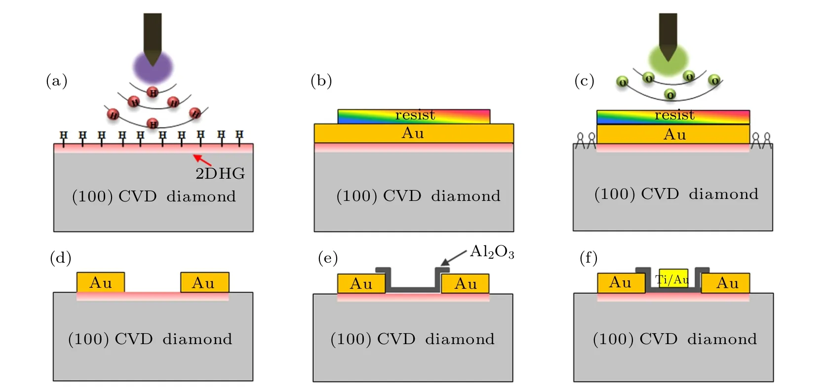
Fig. 1. C–H diamond MOSFET fabrication processes. (a) Hydrogen-termination treatment, (b) deposition of Au to protect H-terminated diamond surface, and preparation of wet etching process of non-device areas, (c) device isolation by using oxygen plasma, (d) formation of source and drain electrodes,(e)ALD deposition of Al2O3 as gate insulator and passivation layer,and(f)gate fabrication and lift-off.
Figure 3(a) shows the measured C–VGcharacteristics of the gate–source capacitance of the Fat-FET devices at 1 MHz.The measured dielectric constants (ε) of Al2O3under 80-°C and 300-°C depositions are 8.75 and 6.78, respectively,which are consistent with the reported values.[20,21]The inset of Fig. 3(a) shows the calculated hole sheet density (np)versus gate voltage by integrating the C–VGcurve. The maximum 2DHG concentrations are 8.7×1012cm−2(300°C)and 1.1×1013cm−2(80°C), respectively. The inset shows that less channel holes exist in the 300°C-deposition diamond device than in the 80-°C case, which is possibly due to the fact that the conduction-related surface adsorbates of C–H diamond decrease with ALD deposition temperature increasing,which was indicated by the reported high-resolution transmission electron microscopy(HRTEM)images.[22]Furthermore,the Mott–Schottky plot is shown in Fig.3(b),from which the flat band voltage(VFB)was determined by linear extrapolation of the 1/C2–VGcurves to the abscissa.The background acceptor concentration (NA) extracted from the linear slope[23]are 1.1×1013cm−3and 2.2×1013cm−3for 80°C and 300°C,separately. The values suggest the high purity of the diamond samples. Taking into account the difference in work function between Al (4.3 eV) and C–H diamond (4.9 eV),[24]the theoretical flat band voltage (VFB0) was calculated to be 0.6 V.As indicated in Fig. 3(b), the measured VFBvalues for 80-°C and 300-°C depositions were 0.42 V and 0.74 V,respectively.According to Qox=Cox×(VFB−VFB0)/q, the fixed charges in the oxide layer(Qox)were estimated to be 8.7×1011cm−2(80°C) and −5.9×1011cm−2(300°C). The negative fixed charges in the Al2O3deposited at 300°C could be due to some unoccupied levels in the bandgap of Al2O3located near the valence band edge of diamond.[25]The positive fixed charges observed in the 80-°C deposition device may be attributed to the oxygen vacancies in the oxide films.[26]

Fig.2. Topview SEM images of 0.1-µm LG:(a)80-°C deposition device and(b)300-°C deposition device.
The DC tests (ID−DC) show that both diamond devices’ maximum drain currents exceed −400 mA/mm (LG=0.1µm), the IDS–VGScurve of the 80-°C and 300-°C deposition devices at VDS=−8 V are shown in Fig.4. Owing to the higher dielectric constant of the 80-°C deposition ALD Al2O3film,the device has exhibited better subthreshold performance.Pulsed I–V test is more effective than DC I–V measurement to characterize the traps-related performances because of its discontinuous signal excitation. Comparatively speaking, there is more severe current degradation in the 80-°C deposition diamond device when it is operated in the pulse I–V mode as shown in Fig. 5. Specifically, pulsed I–V (ID−pulse) measurements are employed to characterize the response of trap charging/discharging for the 0.1-µm-LGdiamond MOSFETs(VGSQ=5 V,VDSQ=−8 V).If the time constant of the charged traps is smaller than the pulse width, reduced holes and thus reduced current will be observed due to insufficient time for discharging from traps.[27]Figure 6 shows the ID−pulse/ID−DCcharacteristics measured at VGS=−2 V and VDS=−6 V.During the measurements, the pulse period used is 1 ms and the pulse width varies from 1µs to 100µs. For the 80-°C deposition device,a much more serious current degradation is observed, which suggests that it has more donor-like traps with a time constant smaller than 100 µs. In addition, it is worth noting that the drain current densities of the 300-°C deposition device in this work is the highest in the reported C–H diamond MOSFETs with 300-°C deposition ALD Al2O3.[14,19]

Fig. 3. (a) C–VG and (b) 1/C2–VG characteristics of the Al2O3/C–H diamond capacitor measured at 1 MHz and room temperature (RT). VFB of 0.42 V and 0.74 V are measured at 80-°C and 300-°C depositions, respectively,and VFB0 of 0.6 V is the theoretical value,it is fitting with the formula 1/C2=(−2/εε0eNA)(V −VFB+kT/e).

Fig.4. DC IDS–VGS curve of 80-°C and 300-°C deposition 0.1-µm-LG devices at VDS=−8 V.
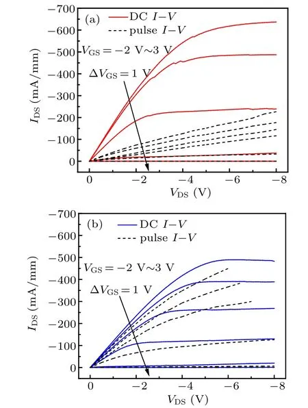
Fig.5. DC and pulsed I–V characteristics of(a)80-°C and(b)300-°C deposition diamond MOSFETs. In pulsed I–V case, quiescent bias point is selected at VGSQ=5 V,VDSQ=−8 V,and pulsed period and width are 1 ms and 1µs,respectively.

Fig.6. Ratio of pulse current to DC current(ID−pulse/ID−DC)characteristics of 80-°C and 300-°C deposition devices at VGS =−2 V and VDS =−6 V,with inset showing applied waveform during pulse I–V measurement.
3. The interface trap mapping by conductance method
In general, emission, rather than capture, is the rate limiting process.[28]Thus characterization of the trap emission time constant(τit)in diamond is crucial to the understanding of the interior trap behaviors. The frequency-dependent conductance method,proposed by Nicollian and Goetzberger,[28]is used to determine the interface traps behavior. The inset of Fig. 7 shows (a) the equivalent circuit of the measured MOS structure,where Cmand Gmdenote the measured capacitance and conductance, respectively; (b) the equivalent circuit of the MOS structure used for the conductance method,where Cit=qDitis the interface trap capacitance when Ditis given in eV−1·cm−2,Ritrepresents the energy loss caused by the capture-emission of carriers by interface trap, τit=RitCitis the interface trap time constant; (c) the simplified circuit with equivalent parallel conductance(Gp). In particular,series resistance (Rs) is introduced into the equivalent circuit considering high contact and access resistance of C–H diamond devices.[29]

Fig.7. Experimental data(circles)and fitting curves(lines)of Gp/ω ~ω.Plotted Gp/ω ~ω results of the 80-°C(left)and 300-°C deposition(right)devices are selected in their subthreshold bias regions. Inset shows(a)measured and[(b),(c)]equivalent circuits of MOS structure,correcting for series resistance(Rs)of contact resistance and access resistance of diamond FETs.
The Gp/ω ~ω characteristics at the selected voltages can be determined from Cmand Gm,[28]which can be expressed as

where Coxof 0.78 µF/cm2and 0.60 µF/cm2were extracted from the C–VGcharacteristics of the 80-°C and 300-°C deposition devices,respectively,

with ω =2π f being the radial frequency, Rsis the series resistance and determined from

Here,Gmaand Cmaare the measured conductance and capacitance in the accumulation mode. By assuming continuous interface trap levels,Gp/ω can be given by

where q is the elemental charge,and Ditdenotes the trap density. Mapping of Ditand τitcan be achieved by fitting the experimental Gp/ω ~ω data through using Eq.(5)as shown in Fig.7. For Eq.(5),the peak point(Gp/ω)maxis located at ωτit=2, and Ditcorrelated with (Gp/ω)maxequals (2.5/q)(Gp/ω)max. It can be seen that the measured conductance peaks of the 80-°C deposition device are broader than those predicted by Eq. (1), which was also observed in the nonannealed MOSFETs.[30]From Fig. 7, it can be seen that the 300-°C ALD process on the C–H diamond surface results in the suppression of the oxide charge non-uniformities and a higher interface quality. According to the Shockley–Read–Hall (SRH) statistic model,[28]the trap energy levels above diamond valence band(Eit–EV)can be deduced from the trap time constant(τit),which is written as

where vthis the thermal velocity,σpis the hole capture cross section, and NVis the effective density of states in diamond valence band. By assigning T =300 K, vth=1×107cm/s,σp=4×10−13cm−2,and NV=2.7×1019cm−3,figure 8(a)shows the mapping results of the trap density distributions and the corresponding energy levels, indicating that shallow traps(Eit−EV≈0.46 eV–0.56 eV)exist in diamond devices.Specifically,Ditin the 80-°C deposition device is in a range of 7.8×10¹³eV−1·cm−2–8.5×10¹³eV−1·cm−2for an energy level span of 0.46 eV–0.52 eV above the valence band of diamond. The higher trap density in the 80-°C deposition device is consistent with the results obtained from the above pulse I–V analysis. The devices with high interface traps may suffer the weak Fermi-level pinning (WFLP) effect, which will make the majority of charges in the MOS capacitor accommodated by interface traps, and cannot be found to operate as a classic MOS capacitor.[31]Notably,besides the depletion and accumulation performances in the C–V curves(Fig.3(a)),the typical current–voltage on/off characteristics (Fig. 4) can be observed for both devices. That is to say, the potential influence of the WFLP effect on our devices is generally acceptable. For the 300-°C deposition device, Ditis in a range of 2.2×10¹³eV−1·cm−2–5.1×10¹³eV−1·cm−2, with the energy level span of 0.53 eV–0.56 eV above the valence band of diamond. In fact, diamond material is expected to have deep energy level interface traps with long τit.[12]According to the SRH model,relation between the detectable trap energy range in the band gap of diamond (5.5 eV) and the correlated τitis shown in Fig.8(b). Notably,by using the conductance method at RT, only a small part of the trap states in diamond can be detected, and the calculated τitis around 1 year for the nearmidgap trap states even at 300°C(the grey line).
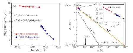
Fig.8. (a)Energy distributions of interface state density of Al2O3/C–H diamond structure,and(b)energy level Eit versus trap emission time constant τit in diamond band gap at RT(orange line)and 300 °C(grey line).
Figure 9 shows the schematic of energy band of the capturing process and emission process of the interface traps with different trap energy levels above the valence band of diamond (at the same gate voltage), and the red line and blue line demonstrate the energy band of the 80-°C and 300-°C deposition devices,respectively. Higher band up-bending of the 80-°C deposition suggests higher carrier concentration in the 2DHG channel, and it contains shallower energy level interface traps(ΔET)while the trap density is higher. As shown in Fig. 9(a), the interface traps capture the carriers when reducing VG. Figure 9(b)indicates that the filled interface traps with lower ΔETfirst emit the holes to the channel when increasing VG,while those interface traps with higher ΔETare more difficult to emit the holes. The gate leakage current characteristics of both Fat-FETs are shown in Fig.10,it can be noted that the IGSof the 80-°C deposition device begins to increase at the forward bias, while the 300-°C deposition device maintains low IGSin the total VGSrange. This can be attributed to the emission of the trapped holes into the gate electrode as suggested by the Frenkel–Poole (FP) emission effect,[14]since the detected interface trap of the 80-°C deposition device is higher than that of the 300-°C deposition device.
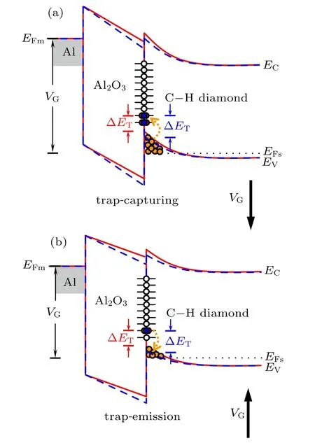
Fig.9. Schematic diagram of band diagrams of the capturing and emission processes of Al2O3/C–H diamond interface traps,where red and blue lines demonstrate the energy band of the 80-°C and 300-°C deposition devices,respectively. (a) Trap capturing with VG decreasing (hole accumulation),and(b)trap emission with VG increasing(hole depletion).
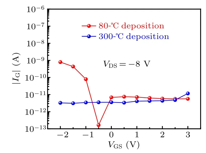
Fig.10. Gate leakage current of 50µm-LG diamond MOSFETs.
4. Conclusions and perspectives
In this paper,the comparative studies by using C–VGand pulse/DC I–V measurements are presented to characterize the traps-induced current degradation in the C–H diamond MOSFETs at different Al2O3deposition temperatures. The results show that while a wide range of ALD deposition temperatures can be used to fabricate diamond FETs with low gate leakage current and high drain current density, different trapped charges can exist in the Al2O3dielectric layer. Experimental results show that 300-°C ALD grown Al2O3can be a suitable gate dielectric and passivation layer solution for the prospective diamond power devices.
猜你喜欢
杂志排行
Chinese Physics B的其它文章
- Corrosion behavior of high-level waste container materials Ti and Ti–Pd alloy under long-term gamma irradiation in Beishan groundwater*
- Degradation of β-Ga2O3 Schottky barrier diode under swift heavy ion irradiation*
- Influence of temperature and alloying elements on the threshold displacement energies in concentrated Ni–Fe–Cr alloys*
- Cathodic shift of onset potential on TiO2 nanorod arrays with significantly enhanced visible light photoactivity via nitrogen/cobalt co-implantation*
- Review on ionization and quenching mechanisms of Trichel pulse*
- Thermally induced band hybridization in bilayer-bilayer MoS2/WS2 heterostructure∗
