Degradation of β-Ga2O3 Schottky barrier diode under swift heavy ion irradiation*
2021-05-24WenSiAi艾文思JieLiu刘杰QianFeng冯倩PengFeiZhai翟鹏飞PeiPeiHu胡培培JianZeng曾健ShengXiaZhang张胜霞ZongZhenLi李宗臻LiLiu刘丽XiaoYuYan闫晓宇andYouMeiSun孙友梅
Wen-Si Ai(艾文思), Jie Liu(刘杰),†, Qian Feng(冯倩), Peng-Fei Zhai(翟鹏飞), Pei-Pei Hu(胡培培),Jian Zeng(曾健), Sheng-Xia Zhang(张胜霞), Zong-Zhen Li(李宗臻), Li Liu(刘丽),Xiao-Yu Yan(闫晓宇), and You-Mei Sun(孙友梅)
1Institute of Modern Physics,Chinese Academy of Sciences(CAS),Lanzhou 730000,China
2School of Nuclear Science and Technology,University of Chinese Academy of Sciences,Beijing 100049,China
3State Key Discipline Laboratory of Wide Band Gap Semiconductor Technology,School of Microelectronics,Xidian University,Xi’an 710071,China
Keywords: β-Ga2O3 Schottky barrier diode,swift heavy ions,reliability degradation,amorphous latent track
1. Introduction
Monoclinic Ga2O3(β-Ga2O3) is a traditional transparent conductive oxide material and β-Ga2O3based photodetectors are attracting interest as truly solar-blind deep ultraviolet photodetectors, since they exhibit cut-off wavelengths below 280 nm.[1,2]This makes β-Ga2O3attractive in the fields of new generation photoconductors, such as deep ultraviolet detectors, light-emitting diodes, and lasers. The research on β-Ga2O3has been extremely hot in the past decade because of its new application in power electronic devices. β-Ga2O3has not only excellent optical properties,but also a large bandgap of 4.7 eV–4.9 eV and a high critical electric field strength of 8 MV/cm.[3]The large bandgap and the high critical electric field strength enable β-Ga2O3based devices to operate at high temperature and high power. Furthermore, β-Ga2O3can be prepared by melting method,which is the same as Si and sapphire substrate. Compared with SiC and GaN,the cost advantage of β-Ga2O3further promotes its application in the field of high-power electronic devices.[4]
The β-Ga2O3devices will face huge challenges used in aerospace systems despite their excellent properties. The radiation environment in outer space comprises high-energy protons,electrons,neutrons,and heavy ions.[5]Then,the different types of damages can be formed in the devices after different particle irradiations. For electrons, protons, and γ-rays irradiations, simple point defects are generally introduced in the wide band gap semiconductors.[6,7]Heavy ions and fast neutrons mainly introduce point defects or cascade displacement damages by elastic collision with target atoms.[8]β-Ga2O3is generally considered to be radiation hardness to displacement damage due to the high bond energy and large band gap.[9]According to the literature, the 4H-SiC single crystal was amorphous at fluence of 0.4 dpa(displacements per atom)for 4 MeV Xe ions irradiation,[10]but the saturate disorder state of β-Ga2O3single crystal can be reached at a higher fluence of 0.6 dpa for 700 keV Sn ions irradiation.[11]Moreover,the irradiation response of carrier concentration in β-Ga2O3Schotty barrier diode(SBD)is similar to that of GaN devices after irradiated by electrons and protons.[12]
Different from the above traditional particles that mainly introduce damages by interaction with the target atoms, the swift heavy ions (SHIs, >1 MeV/u), one of the cosmic rays, mainly transfer energy to the target electrons through huge electronic energy deposition and target electrons further transfer the energy to the atoms through electron–phonon coupling.[13,14]When the electronic energy loss (Se) is large enough, a single swift heavy ion can cause local melting of material and introduce amorphous or recrystallized damage region during quenching. This damage region of nanometer in size is called latent track. In our previous study,it was found that amorphous latent tracks could be introduced in β-Ga2O3single crystal when Seexceeded 17 keV/nm.[15]However,the effect of latent tracks on the electrical characteristics of β-Ga2O3devices is still not studied yet. Therefore, 2096 MeV Ta ions were used to irradiate β-Ga2O3SBD devices in this work and the role of latent tracks on the reliability degradation of devices was analyzed in detail.
2. Experimental details
The vertical β-Ga2O3SBD devices were used in this work. The N−β-Ga2O3(001) drift layer (Sn: ~1.8×1016cm−3) of thickness 8 µm was deposited by hydride vapor phase epitaxy on 1.5 mm bulk N+substrate (Sn: ~3×1018cm−3). The metal stack of Ti/Au was deposited on the whole back of the N+substrate by E-beam evaporation and followed by the rapid thermal annealing at 500°C for 60 s under nitrogen atmosphere to form the Ohmic contact. The front side of the N−drift layer was patterned by lift-off of E-beam deposited Schottky contacts Ni/Au(45 nm/65 nm). The diameter of the Schottky contact was about 100µm. The structure of the schematic across section of β-Ga2O3SBD is shown in Fig.1(a). The β-Ga2O3SBD devices were divided into three groups and named#1,#2,and#3,respectively.

Fig. 1. (a) The schematic across section of the vertical β-Ga2O3 SBD and(b)the distribution diagram of electronic energy loss(Se)and nuclear energy loss(Sn)of 2096 MeV Ta in β-Ga2O3 SBD.
Heavy ion irradiation experiment was performed at the Heavy Ion Research Facility in Lanzhou (HIRFL) in the Institute of Modern Physics (IMP), Chinese Academy of Sciences (CAS). The β-Ga2O3SBD devices without electrical bias were irradiated with 2096 MeV Ta ions in the vacuum chamber. The Seand nuclear energy loss(Sn)were calculated by SRIM 2013 code[16]and the detail distribution of Seand Snin β-Ga2O3SBD was plotted in Fig. 1(b). The range of 2096 MeV Ta ions in the device is about 50µm,reaching deep inside the substrate far away from the metal–semiconductor(M–S) interface. Due to the limited number of samples, cumulative irradiation was adopted in this work. The devices were irradiated for the first time with the fluence of 5×10⁷–5×10⁸ions/cm2,respectively. After irradiation,the irradiated samples were removed from the vacuum chamber for electrical properties measurement. Then they were continued to be irradiated until the fluence up to 1×10⁹–1×10¹⁰ions/cm2,respectively. The specific irradiation parameters are listed in Table 1.
Current density–voltage (J–V) and high frequency(1 MHz)capacitance–voltage(C–V)characteristics were measured by a Keithley 4200 semiconductor parameter analyzer at room temperature.For each fluence,ten Schottky electrodes at least with almost identical electrical characteristics were analyzed.The normal behaviors of J–V and C–V are shown in the next section. The microstructure of β-Ga2O3SBD after irradiation was characterized by bright-field TEM using a Tecnai G2 F20 S-TWIN TEM(FEI,USA)at the accelerating voltage of 200 kV.

Table 1. The irradiation fluence of the three groups of β-Ga2O3 SBD in the first irradiation experiment and the total fluence after the second cumulative irradiation experiment.
3. Results and discussion

Fig. 2. (a) The forward J–V characteristics and the differential onresistance Ron before and after irradiation. (b)The reverse J–V characteristics before and after irradiation. The unit of Ta ions fluence is ions/cm2.
Figure 2(a) shows the forward J–V characteristics and the differential on-resistance Ronas a function of the voltage for β-Ga2O3SBD devices with different ion fluences.The results show that the forward current density decreases gradually with the increasing influence. At the forward bias of 2 V,the maximum current density decreases from 327 A/cm2to 83 A/cm2and the Ronincreases from 3.8 mΩ·cm2to 13.7 mΩ·cm2at the fluence of 1×10⁹ions/cm2. When the ion fluence increases to 5×10⁹and 1×10¹⁰ions/cm2, the β-Ga2O3SBD devices do not exhibit forward guide characteristics and the Ronvalues reach to the order of MΩ·cm2(see Table 2). The reverse J–V characteristic also indicates the increase of the reverse leakage current density as shown in Fig.2(b). It suggests that Ta ions irradiation can significantly affect the J–V characteristics of the β-Ga2O3SBD devices and degrade the performance.
According to the thermionic emission theory,[17,18]the relationship between the voltage and the current density can be described as

where Jsis the saturation current density,n is the ideality factor, k is Boltzmann’s constant, T is the absolute temperature,A*is the effective Richardson constant(41.1 A/(cm2·K2)),and ΦBis the Schottky barrier height. The parameters n and ΦBcan be estimated by fitting the linear region of the J–V curve and the detail electrical parameters of β-Ga2O3SBD devices before and after irradiation are summarized in Table 2. In order to compare the variation of electrical parameters more intuitively, the increment of each parameter (the parameter value after irradiation minus the parameter value before irradiation) is shown in Fig. 3. Since the β-Ga2O3SBD devices do not exhibit forward guide characteristics when the fluence is up to 5×10⁹and 1×10¹⁰ions/cm2, the variations of Von,n, and ΦBin Fig. 3(a) only cover in the fluence range from 5×10⁷ions/cm2to 1×10⁹ions/cm2.
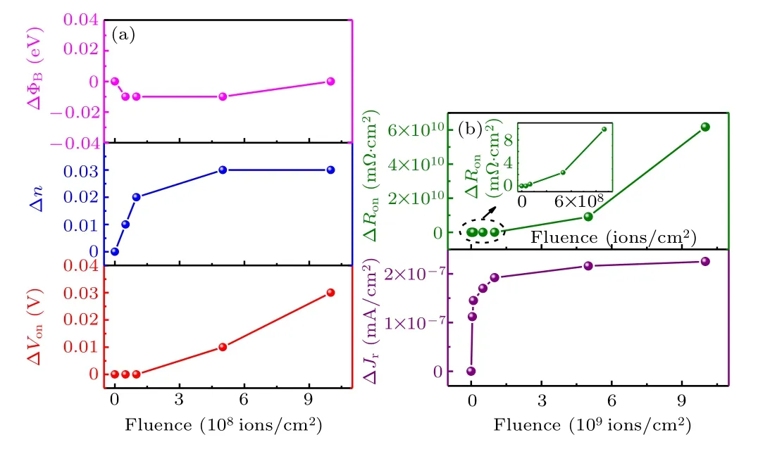
Fig.3. The increments of electrical parameters(turn-on voltage Von,ideality factor n,Schottky barrier height ΦB,reverse leakage current density Jr,and on-resistance Ron)as a function of fluence before and after irradiation.
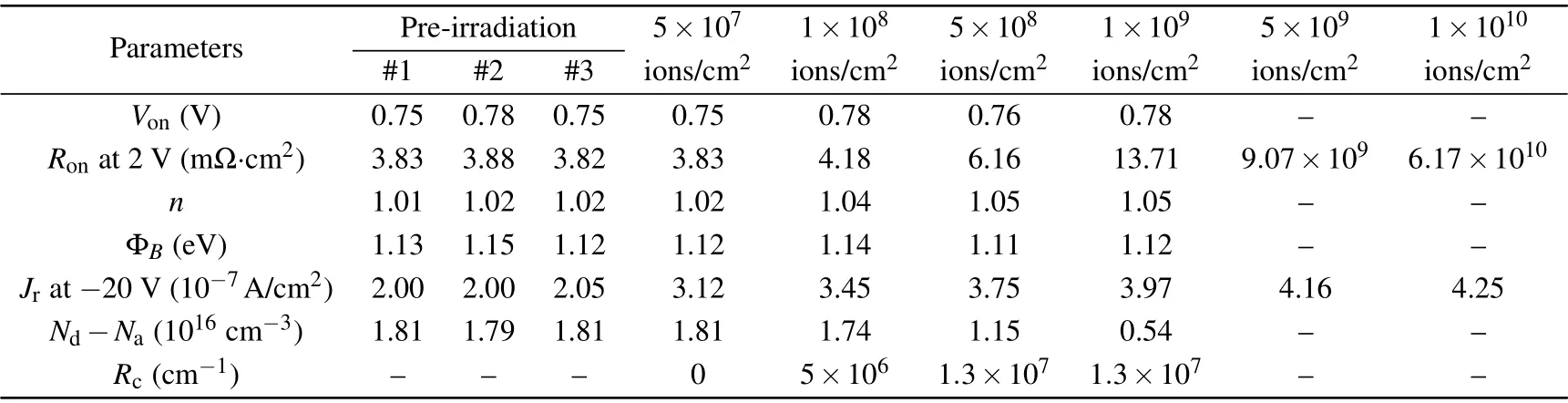
Table 2. Comparison of experimentally calculated values of β-Ga2O3 SBD devices before and after 2096 MeV Ta ions irradiation.
In Fig. 3(a), both of the turn-on voltage Vonand ideality factor n increase with fluence increasing,while the parameter ΦBshows little changes.The increase of ideality factor n indicates that the current transport mechanism gradually deviates from the thermionic emission model. In general, the defects introduced by irradiation can lead to the increase of M–S interface state density and then other current transport mechanisms will participate in the process, such as tunneling.[19,20]The defects can also act as the capture centers of carriers,resulting in the decrease of the carrier concentration and mobility.[21]Hence,the on-resistance Ronvalue increases with the increase in fluence as shown in Fig.3(b). In general,the reverse leakage current density Jrcan reflect the blocking characteristic of SBD. In Fig. 3(b), the increase of Jrafter irradiation indicates the degradation of blocking.This is mainly related to the reduced carrier lifetime due to the increase of deep level recombination centers in the barrier region after irradiation.[22]

Fig.4. The C–V and 1/C2–V characteristics(1 MHz)of the devices after 2096 MeV Ta ions irradiation. The unit of Ta ions fluence is ions/cm2.
Figure 4 shows the C–V and 1/C2–V plots at a frequency of 1 MHz. The C–V relationship for a Schottky barrier is[23]
where q is the electron charge, A is the area of the Schottky diode, ε is the dielectric constant (Ga2O3, ε =10ε0), Vbiis the built-in potential, and Nd−Nastands for the carrier concentration in the drift layer. The carrier concentration can be extracted from the slope of the 1/C2–V curve and the results are listed in Table 2. Only the carrier concentrations in the drift layer are calculated with the fluence range of 5×10⁷–1×10⁹ions/cm2. The corresponding variation of normalized carrier concentration is summarized in Fig.5(a).
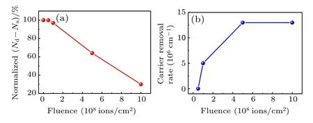
Fig. 5. (a) The normalized carrier concentration and (b) carrier removal rate in the drift β-Ga2O3 layer after 2096 MeV Ta ions irradiation.
According to Fig.5(a),it is clear that the carrier concentration in the drift β-Ga2O3layer shows little changes at the fluence of 5×10⁷ions/cm2. However, the carrier concentration decreases significantly as the fluence increases from 1×10⁸ions/cm2to 1×10⁹ions/cm2. At the fluence of 1×10⁹ions/cm2,the normalized carrier concentration is only 30% that of the unirradiated samples. The acceptor-defects introduced by Ta ions result in the decrease of the carrier concentration, further cause the increase of the depletion width,and finally show that the capacitance in C–V measurement decreases with the increase of fluence. As the fluence increases further to 5×10⁹ions/cm2and 1×10¹⁰ions/cm2,the excessively low carrier concentration is equivalent to the infinite width of the depletion layer and the Schottky barrier capacitance disappears.
According to the carrier concentration, the carrier removal rate Rcis calculated and the results are plotted in Fig. 5(b). The carrier removal rate Rcrelates to the removal of carriers by deep traps which are introduced by the radiation. It is related to the fluence ϕ and the decrease value of carrier concentration Δ(Nd−Na)through the equation[6,24]
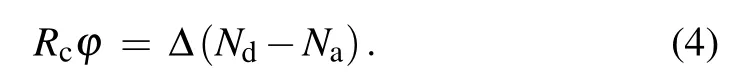
The Rccan provide a practical guide for estimating the degree of the degradation induced in the devices or materials for a given fluence of the common type of radiation. In this work, the calculated Rcis 5×106cm−1for β-Ga2O3SBD irradiated with Ta ions to the fluence of 1×10⁸ions/cm2and it reaches saturation the value of 1.3×107cm−1at the fluence of 5×10⁸ions/cm2. In general, Rcis linear increasing with the fluence at the lower fluence. However,if most of the carriers are removed at a higher fluence,the excess defects will not contribute to the carrier removal effect any more. Thus, the relationship between Rcand the fluence ϕ will not follow the linear relationship.[6]
The carrier removal rates of β-Ga2O3based devices irradiated by different types of ions are summarized in Fig. 6(a)(red symbols).[12,25–27]Note that the carrier removal rate is 406–728 cm−1for α particles irradiation,[27]300 cm−1for 10 MeV protons,[12]4.9 cm−1for 1.5 MeV electrons,[26]and 19–28 cm−1for 1.25 MeV neutrons[25]in β-Ga2O3SBD devices or rectifiers. However,the carrier removal rates for SHIs in this work are much higher. This indicates that the energetic Ta ions exhibit the highest carrier removal rates among these ions irradiation, and it can be explained by the damage type caused by SHIs.

Fig. 6. (a) Carrier removal rate summary diagram in β-Ga2O3 (red symbols)[12,25–27] and other types of GaN or SiC based devices (black symbols)[6,22,28–32] with different species and energies ion-irradiation. The shadow represents the energy regions of swift heavy ions. The data of red star are from our work. (b) The cross-sectional TEM image of β-Ga2O3 SBD irradiated with 2096 MeV Ta ions to a fluence of 1×10¹⁰ ions/cm2.The irradiation direction is indicated by white arrows and the latent tracks parallel to each other are marked by red arrows.
The cross-sectional TEM of the β-Ga2O3SBD irradiated by 2096 MeV Ta ions to a fluence of 1×10¹⁰ions/cm2is shown in Fig.6(b).It can be seen that the interface between Ni and N−β-Ga2O3layer is sharp and there is little inter-mixting at the highest fluence of 1×10¹⁰ions/cm2. However,we find indication of latent tracks parallel to each other in the N−β-Ga2O3layer. In our previous work,[15]TEM results proved that one single 2096 MeV Ta ion introduced the amorphous latent track with a size of ~8 nm in β-Ga2O3single crystal. Considering the range of 2096 MeV Ta ions in β-Ga2O3SBD devices, the latent tracks can be introduced not only in the 8µm N−layer,but also within the range of 40µm in the N+layer. For a single swift heavy ion irradiation, the latent track along the ion trajectory is a nanometer-size amorphous region. For a single proton or α particle irradiation,the introduced damage is isolated atomic-size point defects. Hence Ta ions exhibit the highest carrier removal rate.
Figure 6(a) also summarizes the carrier removal rates of GaN or SiC based devices including SBD devices and high electron mobility transistors(HEMTs).[6,22,28–32]It can be extracted from Fig.6(a)that under the irradiation environment of high-energy electrons,protons,and heavy ions,which mainly introduce displacement damages by elastic collision with the target atoms, the Rcvalues of β-Ga2O3SBD or rectifier are similar to those of GaN or SiC based devices, indicating the excellent radiation hardness of β-Ga2O3devices. This can be attributed to the higher formation energy of vacancy defects in β-Ga2O3.[33–35]However,the degradation of β-Ga2O3SBD is more serious than that of SiC or GaN devices under the SHIs irradiation as the shadow shown in Fig. 6(a).In addition, β-Ga2O3SBD devices in our work are completely damaged under 2096 MeV Ta ions irradiation with fluence of 5×10⁹ions/cm2. However, the GaN HEMTs reported by Hu et al.[36]were still functional after swift heavy Bi ions irradiation with energy of 1500 MeV to the fluence of 1.7×10¹¹ions/cm2.
Based on the thermal spike model,[37]the latent track is formed through the material melting and quenching rapidly along the path of SHIs. Hence, thermodynamic properties and recrystallization ability of the target material are the main factors affecting the latent track formation.[38]The poor thermal conductivity and recrystallization ability of β-Ga2O3make the Sethreshold of latent track formation in β-Ga2O3(17 keV/nm)lower than that of SiC(>34 keV/nm)and GaN(23–28 keV/nm).[15]Therefore, the damage introduced by SHIs in the whole β-Ga2O3matrix has a greater impact on the degradation of β-Ga2O3SBD devices than the damage in M–S interface.
4. Conclusion
We studied the degradation and the structure damages of β-Ga2O3SBD devices after 2096 MeV Ta ions irradiation with the fluence range from 5×10⁷ions/cm2to 1×10¹⁰ions/cm2. Both the conducting and blocking characteristics were sensitive to the ion irradiation. A strong reduction of the carrier was observed and the carrier removal rates were 5×10⁶–1.3×107cm−1. Furthermore, the amorphous latent tracks along the ions trajectories cross the whole area of the drift layer were responsible for the decrease in carrier concentration and mobility, and resulted in the deterioration of the β-Ga2O3SBD devices. In addition,the damage introduced by SHIs in the whole β-Ga2O3matrix had a greater impact on the degradation of β-Ga2O3SBD devices than the damage in M–S interface. The serious degradation of β-Ga2O3SBD indicates the worse radiation hardness of β-Ga2O3based device to SHIs compared with SiC and GaN devices.
猜你喜欢
杂志排行
Chinese Physics B的其它文章
- Process modeling gas atomization of close-coupled ring-hole nozzle for 316L stainless steel powder production*
- A 532 nm molecular iodine optical frequency standard based on modulation transfer spectroscopy*
- High-throughput identification of one-dimensional atomic wires and first principles calculations of their electronic states*
- Effect of tellurium(Te4+)irradiation on microstructure and associated irradiation-induced hardening*
- Effect of helium concentration on irradiation damage of Fe-ion irradiated SIMP steel at 300 °C and 450 °C*
- Optical spectroscopy study of damage evolution in 6H-SiC by H+2 implantation*