High-performing silicon-based germanium Schottky photodetector with ITO transparent electrode∗
2021-03-19ZhiweiHuang黄志伟ShaoyingKe柯少颖JinrongZhou周锦荣YimoZhao赵一默WeiHuang黄巍SongyanChen陈松岩andChengLi李成
Zhiwei Huang(黄志伟), Shaoying Ke(柯少颖), Jinrong Zhou(周锦荣), Yimo Zhao(赵一默),Wei Huang(黄巍), Songyan Chen(陈松岩), and Cheng Li(李成),†
1College of Physics and Information Engineering,Minnan Normal University,Zhangzhou 363000,China
2College of Physics Science and Technology,Xiamen University,Xiamen 361005,China
Keywords: silicon-based Schottky photodetector,germanium epilayer,indium-doped tin oxide
1. Introduction
The tremendous growth in data traffic has now resulted in a great research interest in silicon (Si)-based optical interconnection. In this being, a material with a larger absorption coefficient in near-infrared wavelengths is needed to prepare high-performing photodetectors(PDs).[1-3]Although the high performance compound semiconductors PDs have already been achieved,the stringent packaging requirements of multi-chip implementation lead to a high cost. Germanium(Ge) PDs have many advantages in terms of large optical absorption coefficient at near-infrared wavelengths and fully compatible with the Si-based complementary metal-oxidesemiconductor (CMOS) process. Therefore, Si/Ge PD is regarded as one of the most promising optoelectronic devices for advanced Si photonics.[4-10]
Among the several types of PDs, Schottky PDs have many advantages in terms of speed, long-wavelength detection, and process simplicity.[11-13]Traditional metal/semiconductor Schottky PDs suffer from low quantum efficiency due to the high reflectivity of metal. Fortunately, this problem can be solved by using a highly conductive and transparent indium doped tin oxide (ITO) layer to replace the metal electrode. Recently, high-performing ITO/semiconductor Schottky PDs, such as ITO/GaN,[14]ITO/ZnO,[15]ITO/Si,[16-18]Schottky PDs have been reported.However, to our knowledge, few researches have been done about ITO/Ge Schottky PDs.[19,20]Furthermore, integrating transparent, conductive ITO electrodes into Si-based Ge epilayer to form Schottky PDs has not yet been reported. Some obstacles need to be addressed before the ITO/Ge construction can become a high-performing PD in near-infrared wavebands. On the one hand,a high dark current issue is observed in ITO/Ge PD due to the low Schottky-barrier height (SBH),resulting in poor sensitivity and large power consumption of detector. On the other hand,the absorption coefficient of bulk Ge is still relatively small at 1550 nm when compared to semiconductors such as InGaAs. As a result,Si-based ITO/Ge PDs would suffer from low responsivity when the Ge active region is thin.
In this work,we report a Si(or SOI)-based ITO/Ge Schottky PD with a Si interlayer inserted between ITO and Ge epitaxial layer. A quality rectifying junction is formed for ITO/Si cap/Ge contact. Such PDs show good sensitivity, accredited to effective suppression of dark current. Moreover, benefited from the high transmissivity of ITO electrode and high reflectivity of SOI substrate, the ITO/Si cap/Ge PD shows the excellent photoresponse in NIR regions. The responsivity of the ITO/Si cap/Ge Schottky PDs at 1310 nm and 1550 nm is measured.
2. Experimental details
The Ge epitaxial layers were grown using an ultrahigh vacuum chemical vapor deposition (UHV-CVD) system at base pressures of 5×10⁻⁸Pa. The substrates were highly doped n-type Si (001) wafers with resistivity in the range of 0.002-0.005 Ω·cm, or highly doped n-type SOI wafers with a 1 µm thick top Si and 3 µm thick buried oxide layers. Before epitaxy, the wafers were cleaned by Radio Corporation of America (RCA) method, and the Si surface was baked at 850◦C for 30 min to remove the oxides, followed by about 30 nm Si buffer growing at 750◦C to obtain a clean epiready surface. Then about 90-nm-thick Ge was grown on Si at 330◦C at a growth rate of about 0.50 nm/min. After that,the substrate temperature was raised to 600◦C and 340-nmthick Ge was grown at a growth rate of 1.17 nm/min. The total thickness of the Ge epilayer is about 430 nm, and then about 6-nm-thick Si cap was grown on the Ge epilayer at 390◦C.The sample without Si cap was also prepared under the same conditions for comparison. For further improving the crystal quality of the Ge epilayers,the wafers were treated by furnace thermal annealing at 700◦C or 740◦C for 30 min.
The Si-based Ge epilayer sample,Si-based Si cap/Ge epilayer sample (as-grown), Si-based Si cap/Ge epilayer sample(after furnace thermal annealing at 700◦C),and Si-based Si cap/Ge epilayer sample (after furnace thermal annealing at 740◦C) were used to form contacts with ITO for preliminary evaluating the performance of contact between ITO and Ge epilayer. The schematic diagram of the contacts is shown in Fig.1(a), in which the area of the contacts is about 0.0003 cm2and the thickness of the ITO electrode is about 100 nm.The ITO films were deposited at a DC power of 33 W onto a 60-mm-diameter target (purity: 99.99%, In2O3: SnO2=90:10 wt%)under Ar ambient at 0.3 Pa and room temperature with a deposition rate of 0.08 nm/s.

Fig.1.(a)The schematic diagram of ITO/Si cap/Ge contact.(b)The schematic diagram and(c)metallographic microscope image of SOI-based ITO/Si cap/Ge PD.
The samples of Si- and SOI-based Ge epilayers with Si cap layer after furnace thermal annealing at 740◦C were used to fabricate ITO/Si cap/Ge PDs. The schematic diagram and metallographic microscope image of the device structure are shown in Figs.1(b)and 1(c),respectively. The mesas with the radius from 12µm to 100µm were fabricated by lithographic process.
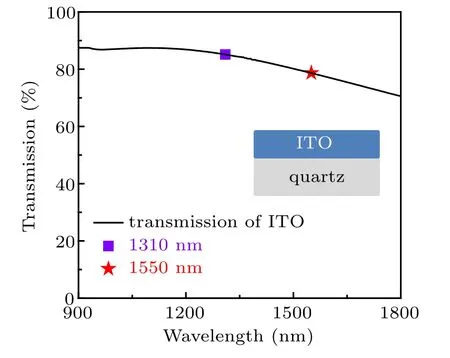
Fig.2. The transmission of ITO film from 900 nm to 1800 nm.
The samples with ITO film on a quartz substrate were used to characterize the transmission property and electrical properties. Figure 2 shows the transmission of the ITO film from 900 nm to 1800 nm acquired by light spectrophotometer. The ITO film exhibits high transmission of 85%and 79%at 1310 nm and 1550 nm, respectively. Table 1 shows the electrical properties of the ITO film analyzed by the Hall effect testing instrument. As shown in Table 1,the resistivity is 9.5×10⁻⁴Ω·cm,the carrier concentration is 4.8×1020cm−3,and the Hall mobility is 14 cm2·V−1·s−1for the ITO film.

Table 1. The electrical properties of ITO.
The surface morphology of the Ge epilayer with Si cap layer samples was analyzed by atom force microscopy(AFM,Seiku Instruments,and SPI4000/SPA-400)in a tapping mode.The strain status and crystal quality of the Ge epilayers were evaluated by double-crystal XRD measurement,using Cu Kα(λKα=0.15406 nm)as the x-ray source. The cross-sectional images of the Ge epilayer with Si cap layer samples were acquired by transmission electron microscopy (JEM2100).The current-voltage (I-V) characteristics were acquired by a Keithley 2611B source/meter.
3. Results and discussion
The atomic force microscopy (AFM) images with a scanned area of 10×10µm2of the Si-and SOI-based Ge epilayers with Si cap layer before and after annealing are shown in Fig.3. The surfaces of the as-grown Si-based Ge epilayer with Si cap layer [Fig.3(a)] and SOI-based Ge epilayer with Si cap layer [Fig.3(b)] are very smooth and the root-meansquare(RMS)surface roughnesses are just 0.9 nm and 1.1 nm,respectively. After furnace thermal annealing at 740◦C for 30 min, the surface morphology of the Si-based Ge epilayer with Si cap layer [Fig.3(c)] and SOI-based Ge epilayer with Si cap layer samples [Fig.3(d)] shows little change and both RMS surface roughnesses are 1.1 nm.
Figures 4(a) and 4(b) show XRD ω-2θ scans and full width at half maximum (FWHM) of Ge (004) XRD patterns for the Si-based Ge epilayer with Si cap layer with different annealing treatments. The diffraction peak of the Si cap layer does not appear in the XRD curve due to its ultrathin thickness and poor crystallization quality when grown at low temperature of 390◦C. The FWHM of the XRD patterns of the annealed Ge epilayers decreases with the increase of the annealing temperature, indicating the improvement of crystallization quality of the Ge epilayer. The strains of the Ge epilayer before and after thermal treatments are obtained using the XRD ω-2θ scans, as shown in Fig.4(c). The biaxial compressive strain in the as-grown Ge epilayer on Si is about 0.1%, while the biaxial tensile strain is increased slightly to 0.11% and 0.12% after furnace thermal annealing at 700◦C and 740◦C,respectively. Figure 4(d)shows XRD ω-2θ pattern for the SOI-based Ge epilayer with Si cap layer sample after thermal annealing at 740◦C for 30 min. The FWHM is measured to be 392 arcsec for the Ge peaks.
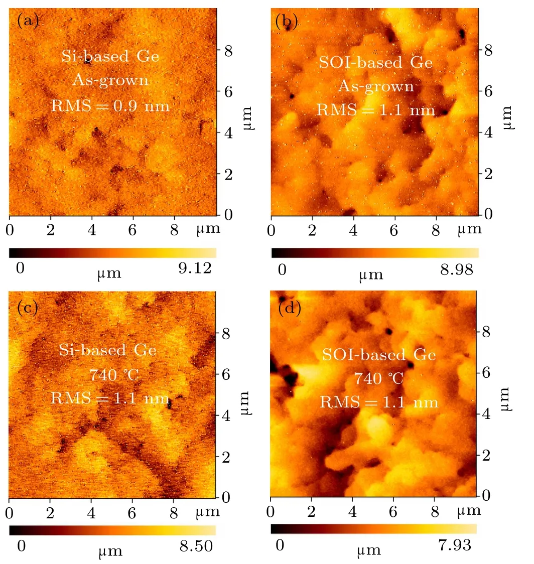
Fig.3. The typical 10×10 µm2 AFM images and corresponding RMS roughness of as-grown (a) Si-based Ge epilayer with Si cap layer and (b)SOI-based Ge epilayer with Si cap layer samples,furnace thermal annealing at 740 ◦C(c)Si-based Ge epilayer with Si cap layer and(d)SOI-based Ge epilayer with Si cap layer samples.
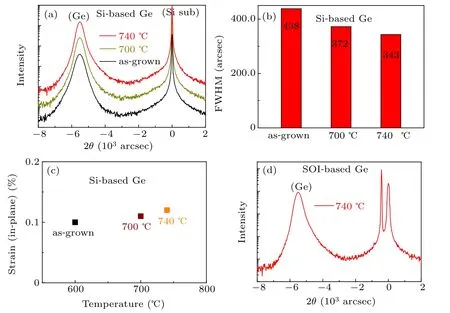
Fig.4. (a)XRD ω-2θ patterns,(b)FWHM,and(c)biaxial tensile strain for Si-based Ge epilayer with Si cap layer samples before and after furnace thermal annealing. (d)XRD ω-2θ pattern for SOI-based Ge epilayer with Si cap layer sample after 740 ◦C thermal annealing.
The typical cross-sectional TEM images for the SOIbased ITO/Si cap/Ge structure is shown in Fig.5, in which the SOI-based Ge epilayer with Si cap layer sample has been thermally annealed at 740◦C before depositing ITO electrode.Figure 5(a)reveals that the ITO and Si cap/Ge layers are uniform,and the film thicknesses of the ITO and Si cap/Ge layers are estimated to be about 100 nm and 430 nm, respectively.Besides,the obvious threading dislocations can be seen in the Ge epilayer as shown in Fig.5(a). The film thickness of the Si cap layer is estimated to be about 6 nm,as shown in Fig.5(b).Figure 5(c)reveals that the interface between the Ge epilayer and top-Si is clear, without apparent Ge-Si intermixing phenomenon.
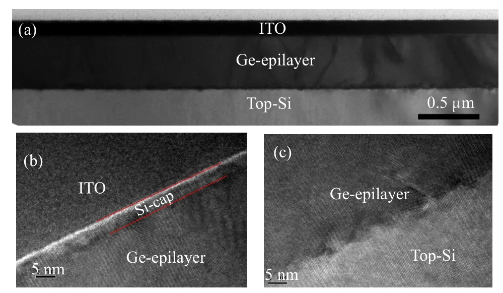
Fig.5. (a)Cross-sectional TEM image of SOI-based Ge epilayer with Si cap layer sample,(b)HRTEM image of ITO/Si cap/Ge interface,(c)HRTEM image of Ge/top-Si interface.
Room temperature dark current voltage characteristics in a semi-log plot for the Si-based ITO/Ge, ITO/Si cap/Ge,ITO/Si cap/Ge (700◦C), and ITO/Si cap/Ge (740◦C) contacts were characterized as shown in Fig.6(a). It is shown that the ITO/Ge contact is quasi ohmic, and the reverse current is slightly greater than the forward current. It is reported that the electron affinity(χ)of ITO is effected by the preparation technology, but overall, the χ of ITO is closed to that of Ge.[19]Therefore,there could be a positive low conduction band offset(ΔEc)between ITO and Ge. In this case,carriers from the Ge will have to surmount a barrier to enter the ITO, which should be responsible for the lower current at forward bias for the Si-based ITO/Ge contact.
By inserting a Si cap layer, the reverse dark current of the ITO/Ge contact significantly decreases, whereas the rectifying ratio increases. This result suggests that the Si interlayer can increase the SBH of the ITO/Ge contact. In addition, figure 6(a) reveals that the reverse dark current of the ITO/Si cap/Ge contacts can be further decreased by adopting Si cap/Ge (700◦C) and Si cap/Ge (740◦C) samples to prepare the contacts. Specially, a well-behaved ITO/Si cap/Ge(740◦C)Schottky contact with a high rectification ratio(about 1120 at ±1 V) and low dark current (1.5×10⁻⁵A at −1 V)is achieved. Such dark current is 610 times lower than that of the Si-based ITO/Ge contact at −1 V bias voltage. The Schottky barrier height(ΦSBH)of the ITO/Si cap/Ge(740◦C)contacts could be extracted from temperature dependent IV characteristics using the activation energy method.[21]Figure 6(b) shows the I-V characteristics of the ITO/Si cap/Ge(740◦C) contact. Figure 6(c) shows extracted lnJ/T2vs.1000/T Richardson plot for the ITO/Si cap/Ge(740◦C)contact. The effective ΦSBHfor the ITO/Si cap/Ge(740◦C)contact is 0.42 eV.
The introduction of Si interlayer and annealing treatment for the Si-based Ge epilayer with Si cap layer have been demonstrated to effectively decrease the dark current of the ITO/Ge contact. The Si- and SOI-based Ge epilayer with Si cap layer samples(after furnace thermal annealing at 740◦C)were used to fabricate vertical structure ITO/Si cap/Ge Schottky PDs. Figures 7(a) and 7(b) show the dark current of the Si-based ITO/Si cap/Ge PDs and SOI-based ITO/Si cap/Ge PDs with different mesa radius. Benefiting from the Schottky contact between ITO and Si cap/Ge, each device clearly establishes rectifying current flows. Overall, the reverse dark current of the SOI-based ITO/Si cap/Ge PDs is higher than that of the Si-based ITO/Si cap/Ge PDs with the same mesa radius.This result could be attributed to the better crystalline quality of the Si-based Si cap/Ge epilayer (740◦C) than that of the SOI-based Si cap/Ge epilayer(740◦C).Specifically,the minimum dark currents of 1.5×10⁻⁷A(corresponding to a dark current density of 33 mA/cm2)and 2.0×10⁻⁷A(corresponding to a dark current density of 44 mA/cm2)were measured for the Si-based and SOI-based ITO/Ge Schottky PDs with mesa radius of 12µm,respectively.
It is also worthy of noting that a jumping phenomenon of current occurs when the forward current of the Si (or SOI)-based ITO/Si cap/Ge PD reaches about 1×10⁻⁷A,as shown in Figs. 7(a) and 7(b). In this paper, a 6 nm Si interlayer is inserted between ITO and Ge. Under forward bias, carriers from the Ge have to surmount a low barrier at the Ge/Si interface to enter the ITO. Since the thickness of the Si cap is only 6 nm,tunneling transport of electrons may occur with the increases of the forward bias,which should be responsible for the jumping phenomenon of the forward current.

Fig.6. (a)Room temperature dark I-V characteristics in a semi-log plot for different contacts,(b)temperature dependent I-V characteristics,and(c)ln(J/T2)vs. 1000/T for Si-based ITO/Si cap/Ge(740 ◦C)contact.
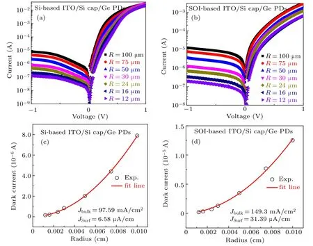
Fig.7. The dark current of (a) Si-based ITO/Si cap/Ge PD and (b) SOI-based ITO/Si cap/Ge with different mesa radius, extracted Jbulk and Jsurf for(c)Si-based ITO/Si cap/Ge PD and(d)SOI-based ITO/Si cap/Ge PD.
The dark current of PDs is related to the bulk dark current density(Jbulk)and the peripheral surface leakage density(Jsurf)through[22,23]

where r is the device mesa radius. As shown in Fig.7(c),the extracted Jbulkand Jsurfof the Si-based ITO/Si cap/Ge PD at −1 V are 97.59 mA/cm2and 6.58 µA/cm, respectively. By contrast, the reverse Jbulkand Jsurfof the SOIbased ITO/Si cap/Ge PDs are higher than those of the Si-based ITO/Si cap/Ge PD.As shown in Fig.7(d), the extracted Jbulkand Jsurfof the SOI-based ITO/Si cap/Ge PD at −1 V are 143.3 mA/cm2and 31.39 µA/cm, respectively. Additionally,it is worthy of mentioning that the dark current densities of the Si-based and SOI-based ITO/Si cap/Ge PDs are larger than those of the reported bulk Ge PDs in literature.[24]For a Ge PD, Jbulkis increased linearly relative to the threading dislocation density in the Ge epilayer.[25,26]Obvious threading dislocations can be seen in the SOI-based Ge epilayer as shown in Fig.5(a), suggesting that there are high density threading dislocations in the Ge epilayer, which should be responsible for the higher dark current density of Ge PDs in this work.
The photocurrents of the Si-based ITO/Si cap/Ge PD(with mesa radius of 100 µm) measured under illumination by 1310 nm and 1550 nm laser light at various powers are shown in Figs. 8(a) and 8(b), respectively. The good distinguishability between the photocurrent and dark current of the Si-based ITO/Si cap/Ge PD can be attributed to its low dark current and excellent light reaction. Besides, it is shown that the photocurrents of the Si-based ITO/Si cap/Ge PD increase with laser power increasing. The responsivity in a Ge PD is related to the optical absorption coefficient(α)and thickness of the active layer(d)of the Ge epilayer through[27]

where λ is the vacuum wavelength,θRis the reflectivity at the input interface,ηinis the internal quantum efficiency,and d is the thickness of the active layer(the thickness of Ge epilayer in this work is 430 nm).
The theoretically calculated external quantum efficiency for the Ge PD at 1310 nm(α=10000 cm−1[28])and 1550 nm(α = 3485 cm−1[25]) are 34.6% and 13.7%, corresponding to the responsivity of 0.37 A/W and 0.17 A/W, respectively.Given the actual value of ηinis lower than 100% and the existence of reflectivity could cause negative effect on responsivity, the experimental values of responsivity would be less than the theoretical ones. Figures 8(c) and 8(d) show the responsivity of the Si-based ITO/Si cap/Ge PD measured under illumination by a 1310 nm and 1550 nm laser,respectively,at different optical powers and a −1 V bias voltage. The experimental optical responsivity is about 0.21 A/W and 0.07 A/W at 1310 nm and 1550 nm, respectively. The decrease of optical absorption coefficient in long wavelength bands should be responsible for the decrease of responsivity at 1550 nm.

Fig.8.(a)Photocurrent of Si-based ITO/Si cap/Ge PD measured under illumination by a(a)1310 nm and(b)1550 nm laser at different powers.Responsivity of Si-based ITO/Si cap/Ge PD measured under illumination by a(c)1310 nm and(d)1550 nm laser at different powers.

Fig.9. (a) Photocurrent of SOI-based ITO/Si cap/Ge PD measured under illumination by a (a) 1310 nm and (b) 1550 nm laser at different powers.Responsivity of SOI-based ITO/Si cap/Ge PD measured under illumination by a(c)1310 nm and(d)1550 nm laser at different powers.
Figure 8(d)shows that the responsivity of the Ge PD decreases with increasing 1550 nm laser power. Germanium is an indirect bandgap semiconductor, whose direct band gap is about 0.8 eV.In this case,the direct band gap of Si-based Ge should be slightly smaller than 0.8 eV,due to the 0.1%biaxial tensile strain.[29]Under illumination by a 1550 nm (0.8 eV)laser,the photogenerated electrons can just jump to the energy state near the conduction band bottom of the direct band. As the laser power increases, the photogenerated electrons and holes increase sharply, resulting in the increase of recombination probability between the photogenerated electrons and holes, which should be responsible for lowering responsivity with 1550 nm laser power. Under illumination by a 1310 nm(>0.8 eV) laser, the photogenerated electrons can jump to higher upper energy states. In this case, the recombination probability between the photogenerated electrons and holes is relatively small. Thus, as shown in Fig.8(c), with increasing illumination power,the responsivity does not decrease.
The photocurrents of the SOI-based ITO/Si cap/Ge PD(with mesa radius of 100µm)measured under illumination by 1310 and 1550 nm laser light at different powers are shown in Figs.9(a)and 9(b),respectively. Overall,the variation tendency of the photocurrents and responsivities of the SOI-based ITO/Si cap/Ge PDs is similar to that of the Si-based ITO/Si cap/Ge PD.The experimental optical responsivity of the SOIbased ITO/Si cap/Ge PD is about 0.26 A/W and 0.19 A/W at 1310 nm and 1550 nm, as shown in Figs. 9(c) and 9(d), respectively. Compared with the Si-based ITO/Si cap/Ge PD,the responsivity of the SOI-based ITO/Si cap/Ge PD becomes larger by about 2.7 times at 1550 nm. The existence of highly reflective between Ge epilayer and SOI substrate can increase the valid optical path of the incident light,which should be responsible for the larger responsivities of the SOI-based ITO/Si cap/Ge PD.
4. Conclusion
In summary, Si (or SOI)-based ITO/Ge near-infrared Schottky PDs were fabricated by inserting a Si layer in the ITO/Ge epilayer contact, in which a junction was formed between ITO and Ge without any intentional doping process for the Ge epilayer. It was demonstrated that the introduction of a Si interlayer and thermal treatment of the Si-based Si cap/Ge epilayer can effectively suppress the reverse dark current for the ITO/Ge epilayer diode. Besides, an excellent photoresponse for long wavelength was achieved by the SOI-based ITO/Si cap/Ge PD, benefited from the high transmissivity of ITO electrode and high reflectivity of SOI substrate. With 430 nm thick Ge epilayer, a minimum dark current of 2.0×10⁻⁷A and an optical responsivity of 0.19 A/W at 1550 nm wavelength were obtained for the SOI-based ITO/Ge Schottky PD.These results are quite useful for the integration of transparent,conductive ITO electrodes into Si(SOI)-based Ge epilayer Schottky PDs that are suitable for detecting the near-infrared wavelength with low cost and high efficiency.
猜你喜欢
杂志排行
Chinese Physics B的其它文章
- Nonlocal advantage of quantum coherence in a dephasing channel with memory∗
- New DDSCR structure with high holding voltage for robust ESD applications∗
- Nonlinear photoncurrent in transition metal dichalcogenide with warping term under illuminating of light∗
- Modeling and analysis of car-following behavior considering backward-looking effect∗
- DFT study of solvation of Li+/Na+in fluoroethylene carbonate/vinylene carbonate/ethylene sulfite solvents for lithium/sodium-based battery∗
- Multi-layer structures including zigzag sculptured thin films for corrosion protection of AISI 304 stainless steel∗
