New DDSCR structure with high holding voltage for robust ESD applications∗
2021-03-19ZiJieZhou周子杰XiangLiangJin金湘亮YangWang汪洋andPengDong董鹏
Zi-Jie Zhou(周子杰), Xiang-Liang Jin(金湘亮),3,†, Yang Wang(汪洋), and Peng Dong(董鹏)
1School of Physics and Optoelectronics,Xiangtan University,Xiangtan 411105,China
2Hunan Engineering Laboratory for Microelectronics,Optoelectronics and System on a Chip,Xiangtan 411105,China
3School of Physics and Electronics,Hunan Normal University,Changsha 410081,China
4Super-ESD Microelectronics Technology CO.,LTD.,Changsha 410100,China
Keywords: dual direction silicon-controlled rectifier(DDSCR),failure current,snapback gate voltage,simulation,transmission line pulsing(TLP)
1. Introduction
With the increasing of complexity of integrated circuit working environment,more and more attention is paid to electrostatic discharging(ESD)protection. Engineers try to meet qualified protection requirements in smaller device area. Silicon controlled rectifier(SCR)is popularly used due to its efficient release capacity per unit area, but the working mechanism of SCR under negative pulse is of diode.[1-3]In the control bus,the signal from the A/B port is bidirectional,the ESD protection should be considered to be also bidirectional, the DDSCR is selected,and the DDSCR device can optimize the ESD characteristics of the DDSCR by changing the structure and size.The deep snapback phenomenon of DDSCR will also cause some problems with high trigger voltage and low holding voltage.[4-7]A novel dual-polarity device were proposed by Salcedo et al. The device meets various ESD protection requirements.The trigger voltage can be adjusted by breakdown junction of DDSCR.[8]Liang et al. proposed a novel gate diode triggered silicon-controlled rectifier(GDTSCR),which greatly improves the holding voltage(4.6 V)of MTSCR.[9]A new high holding voltage dual-direction SCR with optimized segmented GDTSCR which has a strong ESD robustness of 6000 V in an area of 1600µm2is composed of MTSCR,and the GDTSCR has higher trigger voltage(16.5 V)and holding voltage(13.6 V)than the trigger voltage(14.9 V)and holding voltage of the topology proposed by Huang et al.Although the NHHVDDSCR can possess a relatively high and adjustable holding voltage, the failure current is also significantly reduced compared with traditional DDSCR.[10]According to a study by Dong et al.in a novel capacitively coupled complementary bidirectional SCR(CCCDSCR), it was verified that the coupling capacitor can adjust the trigger voltage of the device,and higher holding voltage requires larger layout area.[11]Guan et al. proposed an embedded topology for the highvoltage ESD protection, which greatly improves the holding voltage.[12]Liu et al.proposed an SCR with a stacking structure,the holding voltage can be adjusted to meet different ESD requirements.[13]Dai and Ker found that the Joule-heating effect could dramatically reduce the holding voltage(Vh)of the proposed SCR,and ESD robustness of the proposed SCR device can decrease when a high (Vh) is achieved.[14]Du et al. proposed an enhanced bidirectional modified lateral silicon controlled rectifier (EBMLSCR) and evaluated the effect of some critical dimensions of the EBMLSCR on further optimizing the device performances.[15]Du et al. proposed a compact and self-isolated dual directional silicon-controlled rectifier (CSDDSCR) developed in a single N-well, and the holding voltage reversal effect has also been discovered and explained with technology computer aided design (TCAD)simulation.[16]Do et al. proposed a novel DDSCR structure with a high holding voltage and a low on-state resistance,and the proposed device exhibits a high holding voltage,an excellent current driving capability,and an improved effective ESD tolerance.[17]Liu et al. proposed an SCR which is designed based on the concept that the holding voltage can be increased by reducing the emitter injection efficiency in the SCR.[18]
The studies involved above proved that no matter whether it is a change in structure or in size or adds an additional layer, an increase in the holding voltage will dramatically reduce the failure current.[10,15-18]Others mainly rely on a large area to increase holding voltage within deceasing failure current.[11-13]In this paper,an enhanced dual-direction device(APGDDSCR)is presented. The proposed structure possesses a low trigger voltage, a higher holding voltage, and good robustness. It can avoid the latch-up better without reducing the robustness in dual-direction IO protection.
2. Operation mechanism and simulation of device structure
Figure 1 shows the three-dimensional (3D) layout structure of the conventional LVT-DDSCR (Fig.1(a)),APGDDSCRC (Fig.1(b)), and APGDDSCR (Fig.1(c)) obtained with metal routing.
The LVT-DDSCR is based on conventional DDSCR,and the diode consists of P-well and deep N-well, the breakdown voltage of the diode in the process library is too high for the ESD design window of core circuit. So that the low trigger structure is adopted to reduce the trigger voltage. We also know that the lower trigger voltage will reduce holding voltage,hence,the novel structure APGDDSCR is designed.
Greater cathode and anode spacing can effectively improve the holding voltage of the device,the values of spacing D1 are the same in all structures. The APGDDSCRC is designed for comparison. The equivalent circuits of three structure are shown in Fig.2, and the equivalent circuits of LVTDDSCR are conventional.
The equivalent circuit of (a) the APGDDSCR and (b)the positive and negative ESD stress paths are shown in Fig.2. Compared with the conventional DDSCR, the modified DDSCR has two variable resistors more. They are named RA+and RC+,respectively,marked with a red dashed box and a green dashed box. The heavy N-type doping is not widened.The voltage is applied directly to the gate between P-type doping and N-type doping, which may cause the gate oxygen to break down. Therefore, a heavy doping is added next to the N-type doping region of the anode and cathode, and the gate is design in high voltage design rule. At the same time,in order to form a variable gate voltage without introducing a new parasitic structure, the added region is heavy P-type doping.The gate voltage on gate A is provided by the floating heavily doped P-type doping located in the cathode’s P-well, and the gate voltage on gate C is provided by the floating heavily doped P-type located in the anode’s P-well. When the ESD event happens to the anode in Fig.2(b),the current discharge path is indicated by the red arrow,and the negative discharge path is indicated by the green arrow when the ESD event happens to the cathode. In a positive way, when the voltage applied to the device is sufficiently high for avalanche breakdown of the P-well where the cathode is located and the reversebiased diode formed by the P-type heavily doped region across the P-well,the SCR formed by the parasitic transistor PNP and the parasitic transistor NPNc will turn on.The floating heavily doped P-type that is located in the anode’s P-well is too close to the anode,so the voltage on gate C is essentially equivalent to the voltage applied to the device,and thus the gate C has the same effect as an isolation oxide. But the voltage on gate A of APGDDSCR will increase with the current increasing after the breakdown of the device.Therefore,the voltage on gate A will attract electrons under gate A,and the main carrier of current is electrons.
The SCR turn-on condition is as follows:

where βPNPis the current gain of PNP and βNPNis the current gain of NPN. Reducing the recombination rate of electrons flowing through the device structure is also a method of increasing the current gain. The less the electrons need recombining, the higher the current gain is; the more the electrons need recombining; the lower the current gain is. The voltage on APGDSCR gate A will make the inherent multi-carrier holes in the P-well under the gate A attracted to the inherent minority carrier recombination. Therefore, the number of recombination electrons flowing through the surface of P-well will decrease,so for PNP,the current gain βPNPwill increase,and SCR will be more easily turned on when the current gain of βNPNis unchanged.
At the same time,reducing the recombination of electrons in the current will also increase the current,the current of SCR can be expressed by the current gain of bipolar transistor as follows:

where ICP0is the leakage current of PNP and ICN0is the leakage current of NPN.
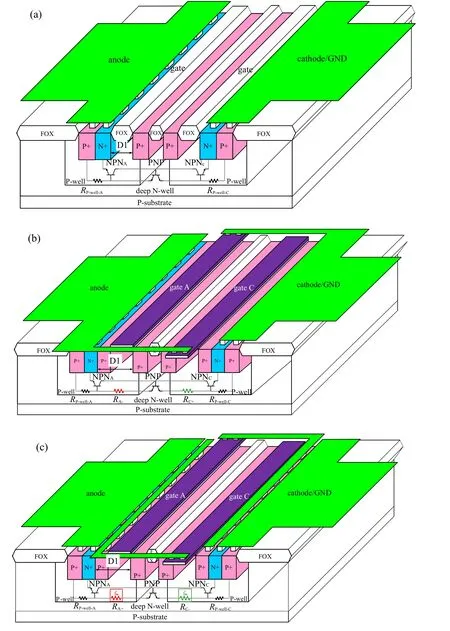
Fig.1. Schematic diagram of 3D layout structure of(a)LVT-DDSCR,(b)APGDDSCR-C,and(c)APGDDSCR.
The increase of βPNPwill lead current I to decrease.The APGDDSCR has a larger holding current than the APGDDSCRC.
At the same time, the LVT-DDSCR with the same size and the contrast group APGDDSCRC with constant voltage on the gate are also designed in this paper.
The Atlas 2D device simulator by Silvaco Corporation is used to verify the operation process of the new structure. Figure 3 shows the total current density distributions of LVT-DDSCR (Fig.3(a)), APGDDSCR (Fig.3(b)), and APGDDSCRC (Fig.3(c)) in direct current (DC) simulation.The total current density distribution is obtained by the current density distribution of each simulation point. The LVTDDSCR,APGDDSCR,and APGDDSCRC have the same current discharge path,and the high light of current of them is in the same node.
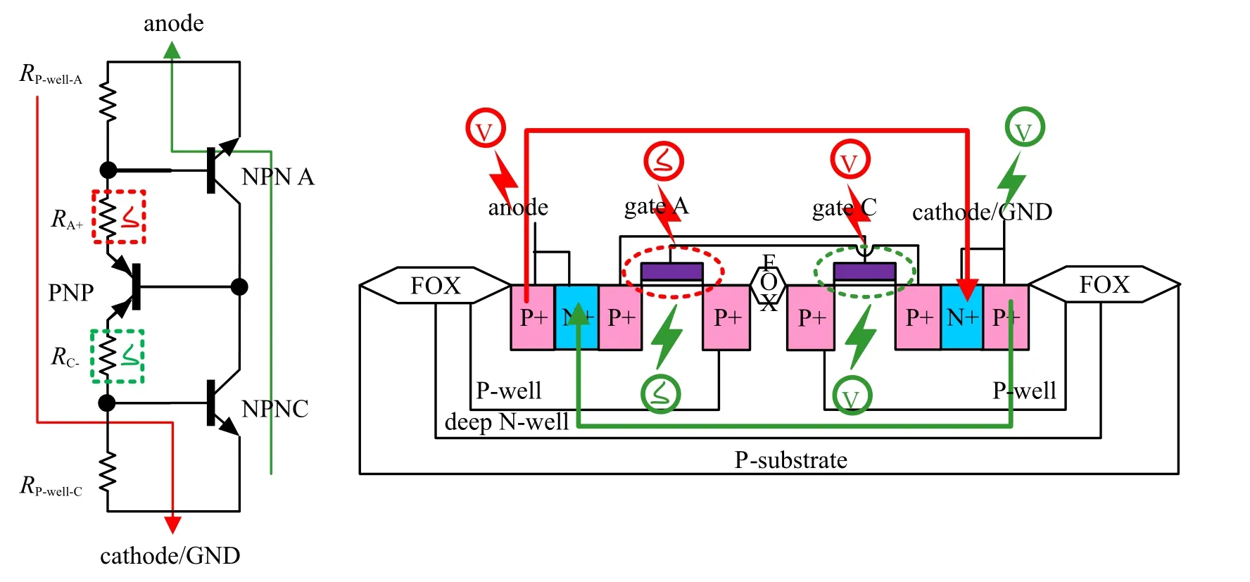
Fig.2. Equivalent circuit of(a)APGDDSCR and(b)e positive and negative ESD stress paths.

Fig.3. TCAD simulated total current density distribution of (a) LVTDDSCR,(b)APGDDSCR,and(c)APGDDSCR-C.
It indicates that the improved device will not be much different from the conventional device in robustness. And the simulated current-voltage(I-V)curve trace is shown in Fig.4,we do not know the doping,nor the depth of junction nor others process parameters of this library,we set the concentration range of heavy doping to be approximately 1019cm−3, the concentration range of the well is 1015cm−3to 1017cm−3,and the doping concentration of the P-substrate is 1014cm−3,and the taup0 and taun0 in material are both 1×10⁻⁷, etc.Simulation cannot offer an accurate result, but we can predict the trend through the simulation results. Figure 4 shows that the modified device has a holding voltage 3.86 V higher than 2.13 V that the conventional LVT-DDSCR has, but the new device also increases the trigger voltage(Vt1). The difference among the three structures is that the voltage on gate A in APGDDSCR will attract electrons under gate A,the main carrier of current is electrons. One current path generated under gate A is shown in Fig.3(b).

Fig.4. The TCAD simulated I-V curve trace of LVT-DDSCR and APGDDSCR.
The variations of voltage of gate A and gate C with the anode int. voltage at APGDDSCR are shown in Fig.5. The simulation results are in line with our expected results. The gate voltage of gate C is provided by the floating heavy P-type doping in anode PW. Since P-type is against the anode, the gate voltage of gate C is the voltage of the anode. The voltage of gate A is provided by the floating heavy P-type doping in the cathode P-well. Since the negative resistance occurs after the SCR has been turned on,the voltage on the floating heavy Ptype doping in the cathode P-well also decreases,which leads the voltage to fall down. The voltage on gate A is lowered.The decrease in voltage on gate A will affect the change in concentration in the area under gate A,so this phenomenon is described as a variable resistance.
Comparing the LVT-DDSCR (Fig.3(a)) and the APGDDSCR-C (Fig.3(c)), we can know that the working mechanism of LVT-DDSCR is similar to that of the APGDDSCR-C.During the period from SCR turn-on to SCR failure, the gate voltage of gate C is provided by the anode,and the voltage of gate A is provided by the cathode. The anode voltage controls gate C,gate C repels the current passing through it. It has the same effect as the isolation oxide of LVT-DDSCR at the same position. The cathode voltage controls gate A, but SCR has a deep current path at the anode,The gate A also has the same effect as the isolation oxide of LVT-DDSCR at the same position.
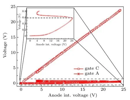
Fig.5. Variation of voltage of gate A and gate C with anode Int. voltage at APGDDSCR.
Comparing APGDDSCR(Fig.3(b))with APGDDSCR-C(Fig.3(c)),gate C for each of these two devices has the same effect as the isolation oxide. The voltage on the gate A of APGDDSCR-C is provided by the cathode,and it has the same effect as the isolation oxide. But the voltage on the gate A of APGDDSCR is provided by the floating heavy P-type doping in the cathode P-well, it brings about the variable resistance phenomenon. The phenomenon is confirmed by the gate A voltage varying with the anode current at APGDDSCR and APGDDSCR-C as shown in Fig.6.
Figure 6 shows that the voltage on gate A of APGDDSCR-C is always zero as the current increases, and at the same time, the voltage on gate A of APGDDSCR increases as the current increases. As is well know,the voltage on gate A appears after the device has broken down and produced a current. When APGDDSCR breaks down, the SCR forms and negative resistance appears. The region between the trigger voltage point and the holding voltage point is called the holding region, and has a very low resistance. When the APGDDSCR starts to discharge after holding voltage point,the region with a larger resistance is called the discharge region.
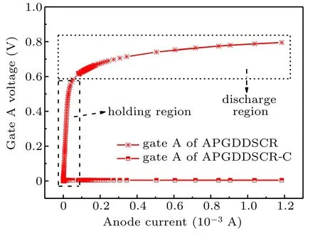
Fig.6. Variation of gate A voltage with anode current at APGDDSCR and APGDDSCR-C.
The APGDDSCR has the highest holding voltage, followed by APGDDSCR-C or LVT-DDSCR, and their holding voltages are similar to each other. The conclusion is also confirmed in the I-V curve trace of Fig.7. It can also be found from the I-V curve trace in Fig.7 that the improved device APGDDSCR has the highest trigger voltage,followed by APGDDSCR-C and LVT-DDSCR.
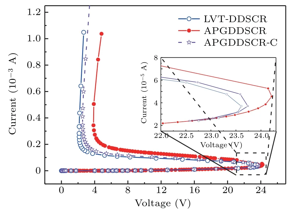
Fig.7. The TCAD simulated I-V curve trace of LVT-DDSCR,APGDDSCR,and APGDDSCR-C.
Figure 8 shows the difference in breakdown area among the conventional DDSCR,LVT-DDSCR,APGDDSCR-C,and APGDDSCR. Figure 8(a) shows the breakdown area of conventional DDSCR,the width(W)of low doped region formed by pn junction, the width (Xm) of the barrier region when the pn junction breaks down, the width (E(x)) of the low doped region formed by pn junction,which is named the electric field strength change. When W is greater than Xm, the breakdown voltage will be determined by the doping concentration. When the breakdown voltage is higher than the designed window,the increased cross-well heavy P-type doping can be used to reduce the breakdown voltage, which is shown in Fig.8(b). The heavy P-type doping changes the width of low doped region formed by the pn junction, the new width is W1: the W1is less than Xm. In the case of a lower external bias voltage, the barrier area fills or exceeds the low doped region formed by pn junction. At this time,the low doped region formed by the pn junction does not increase with the external bias voltage increasing,but the electric field strength increases as the external bias voltage increases.Under the same external bias voltage conditions, the area of the electric field strength function curve should be equal.Therefore,when W1is less than X,the electric field strength is larger,and the reverse breakdown voltage is lowered.

Fig.8. Four breakdown areas: (a) breakdown area of conventional DDSCR, (b) breakdown area of LVT-DDSCR, (c) breakdown area of APGDDSCR-C,and(d)breakdown area of APGDDSCR.

Fig.9. TCAD simulated at trigger point of hole concentration(cconc.) of(a)LVT-DDSCR,(b)APGDDSCR-C,and(c)APGDDSCR.
The improved structure will affect the breakdown area.The breakdown area of APGDDSCR-C and the breakdown area of APGDDSCR are shown in Figs. 8(c) and 8(d). The difference between Fig.8(c) and Fig.8(d) is the voltage applied to the gate. In Fig.8(c),the W2is basically equal to W1.
In a positive way,the external bias voltage is directly applied to the gate and is less than or equal to the breakdown voltage. The gate C which is connected with the anode has the same effect as the isolation oxide. This phenomenon is also confirmed in the simulation as indicated in Fig.7, and figure 9(b) has the same hole distribution as Fig.9(a). Because the area enclosed by the dark green dotted line in Fig.9(c)is less than those in Figs.9(a)and 9(b),the breakdown junction in Fig.9(c) has the smallest concentration gradient on both sides of the junction in each of the three structures. A small concentration gradient means that under the same reverse voltage,the width of the space charge region is wide and the maximum electric field intensity is weak, so the voltage required to achieve avalanche breakdown is high. A PN junction with a definite concentration gradient on both sides of the junction has a depletion region with a definite width. The isolation oxide in Fig.9(a) occupies the position of the depletion layer,making the depletion layer of LVT-DDSCR deeper.The gate C in Fig.8(c)has the same function as isolation oxide,and also makes the depletion layer of APGDDSCR deeper. With the resistor in Fig.8(d), by reducing the voltage on the gate C,the hole concentration near the P-well side of the breakdown junction decreases and the depletion layer moves upward,thus reducing the difference in concentration between the two sides of the breakdown junction and increasing the trigger voltage.The trigger voltage is higher in Fig.8(d),which means that W3is larger than W1or W2.
3. Results and discussion
The APGDDSCR, the APGDDSCR-C, and the LVTDDSCR are fabricated through a 0.5-µm complementary metal-oxide semiconductor(CMOS)process. Each of all devices has a finger width of 80µm. The I-V characteristics are measured and demonstrated by using a transmission line pulsing(TLP)tester with 200-ps/10-ns rise time and 100-ns pulse width.
3.1. Comparison of design window and the robustness between APGDDSCR and LVT-DDSCR
The measured TLP I-V and leakage characteristics of the APGDDSCR and LVT-DDSCR with 200-ps/10-ns rise time are shown in Fig.10.
Fig.10. Measured TLP I-V and leakage characteristics of LVT-DDSCR GATE and APGDDSCR with one finger.
The APGDDSCR possesses a higher positive and negative Vt1of 22.532 V and 23.434 V than the LVT-DDSCR(19.811 V and 19.573 V) which is shown in Table 1. For a 12-V IO pin of the 0.5-µm process used, the holding voltage should be larger than 13.2 V with a 10% safety margin consideration. Therefore, the novel APGDDSCR can be used as an effective ESD protection solution for ±12-V IO ports by solving the high trigger voltage issue through using traditional DDSCR structure. Besides, the APGDDSCR is latch-up free as its holding voltage (about 13.2 V with a 10% safety margin consideration) is much higher than the lower limit of the design window.

Table 1. Comparison of ESD performance among different structure devices.
The leakage characteristics of the two DDSCRs are comparable. It is worth mentioning that the failure current (It2)of LVT-DDSCR and APGDDSCR are almost the same. The APGDDSCR increases the holding voltage without reducing the failure current. Although it increases the trigger voltage,the new structure does work at holding voltage.
3.2. Comparison of effects of multi-finger changes in devices
Increasing the finger of the device is an effective way to improve the device failure ability. Figure 11 shows the TLP test curves of the three different fingers of APGDDSCR.And Table 2 shows the comparison of ESD performance among different structure device. Since the DDSCR structures have the same current path, the forward and reverse TLP curves have better symmetry. At the same size, the APGDDSCR 1F has positive and negative trigger voltages of 22.532 V and 23.434 V, positive and negative holding voltages of 18.781 V and 18.912 V, and positive and negative failure currents of 6.23 A and 6.22 A, respectively. The positive and negative trigger voltages of APGDDSCR 2F are 22.948 V and 22.158 V, the positive and negative holding voltages are 18.349 V and 18.080 V, and the positive and negative failure currents are 8.67 A and 7.95 A, respectively. Comparing the trigger voltages of APGDDSCR 1F and APGDDSCR 2F, it can be found that the values of their trigger voltages are almost the same, but the holding voltages decrease and the failure currents increase.From single finger to double finger, the failure current is not doubled, so the device turns on nonuniformly. The positive and negative trigger voltages of APGDDSCR 4F are 21.862 V and 22.104 V, the positive and negative holding voltages are 14.460 V and 14.319 V, and the positive and negative failure currents are 14.854 A and 15.630 A, respectively. The trigger voltage remains the same value, and the holding voltage and the failure current change regularly. By the way,the LVTDDSCR 1F has 13.371 V and 14.038 V of positive and negative holding voltages,multiple fingers will bring about a lower holding voltage.

Fig.11. Measured TLP I-V and leakage characteristics of APGDDSCR with one finger,two fingers,and four fingers.
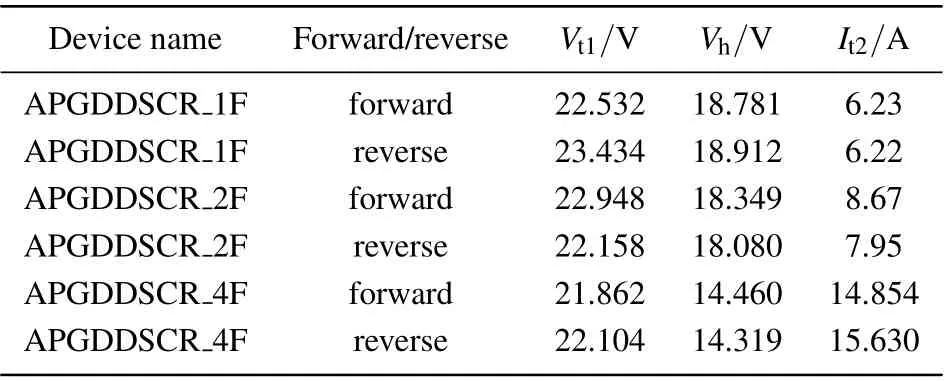
Table 2. Comparison of ESD performance among different structure devices.
Table 3 and Table 4 show the comparison of ESD performance among different structure devices under the second breakdown voltage(Vt2)of 30 V and 40 V,respectively. The failure capacity of APGDDSCR basically increases in proportion to the finger number. And the increase of the finger number can effectively solve the problem about excessive onresistance of the device.
To evaluate the ESD protection performances of various ESD devices,the following defined advantage(FOM)is used:

where It2is the failure current,Vhis the holding voltage,W is the width of the device,N is the finger number of the device,and Vt1is the trigger voltage.
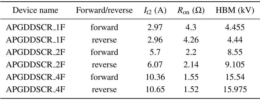
Table 3. Comparison of ESD performance among different structure device under Vt2 of 30 V.
Table 4 shows the FOM and the HBM with different finger numbers. The nonuniform triggering of the device will lead to the problem that the device’s current discharging capacity per unit area decreases with the finger number increasing. Although the finger number of APGDDSCR 2F increases,the FOM of APGDDSCR-2F is almost the same as that of the single finger. The APGDDSCR 4F has a better HBM, but its FOM is lower than other fingers’. Because the new structure has an appropriate trigger voltage and holding voltage, we can make a tradeoff between failure and layout area.

Table 4. Comparison of ESD performance among different structure devices under Vt2 of 40 V.
3.3. Comparison of APGDDSCR with APGDDSCRC
The APGDDSCR 4 and APGDDSCR-C4F are compared as shown in Fig.12 and Table 5. The APGDDSCR4F and APGDDSCR-C 4F have the same structures, the difference between them is that the gate of APGDDSCR-4F connects to the P-type region and the gate of APGDDSCR-C-4F connects to the electrode.
In a positive way, the gate which is nearby cathode repels the current when the device works in APGDDSCR-C 4F.But the gate which is nearby cathode attracts the current when the device works in APGDDSCR 4F and the gate increases the surface electron concentration of P-well. Therefore, a larger current will be needed to allow the same hole to flow through the P-well region, and the APGDDSCR 4F needs higher holding voltage to keep it stable. The holding current of APGDDSCR-C and APGDDSCR are shown in Table 5,and APGDDSCR has a higher holding current than APGDDSCRC.

Table 5. Comparison of ESD performance among different structure devices.
The forward TLP test curves of APGDDSCR and APGDDSCR with four fingers are shown in Fig.12. The APGDDSCR 4F has positive and negative trigger voltages of 21.862 V and 22.104 V, positive and negative holding voltages of 14.460 V and 14.319 V, and positive and negative failure currents of 14.854 A and 15.630 A, respectively. The APGDDSCR-C 4F has positive and negative trigger voltages of 19.57 V and 19.6 V,positive and negative holding voltages of 7.4 V and 7.6 V,and positive and negative failure currents of 14.9 A and 15.7 A,respectively. The gate which is connected to the electrode in APGDDSCR-C does not affect trigger voltage, but the gate which is connected to the P-type region increases the trigger voltage. Different holding voltages prove that the new structure does affect the holding voltage,and different failure currents demonstrate that the new structure only affects the device holding voltage.

Fig.12. Measured TLP I-V and leakage characteristics of APGDDSCR and APGDDSCR-C with four fingers.
The problem about non-uniform triggering will reduce the failure ability of multi-finger devices. We need more fingers in order to achieve a higher failure capability. However,the increase of finger number will lower the holding voltage of device. At the same time, increasing the holding voltage will lead to the problem about reducing the failure current capability. The device designed in this paper can increase the holding voltage without reducing the failure current capability, so even if the finger number of device increases, the reduced holding voltage can meet the requirements for the protected circuit. The APGDDSCR-C is similar to LVT-DDSCR,and the APGDDSCR-C 4F can reach 14.9 A in a positive way and 15.7 A in a negative way. But the positive and negative holding voltages are only 7.4 V and 7.6 V, respectively. At the same time, the APGDDSCR 4 can achieve 14.854 A and 15.630 A in positive and negative way, and the positive and negative holding voltages are 14.460 V and 14.319 V.A higher holding voltage without lowering the failure current is equivalent to solving the problem about the non-uniform triggering of multi-finger devices.
4. Conclusions
In this work,a proposed DDSCR with high holding voltage is realized and discussed in 0.5-µm CMOS process technology. The additional P-type region and gate bring about a variable resistance phenomenon and allow the conventional DDSCR to increase the holding voltage without reducing the failure current, and the new structure is verified through experiments and analyses. Because of the high holding voltage, we can make a trade-off between failure and layout area after discussing the finger number of APGDDSCR. The APGDDSCR 2F has the biggest FOM and a better It2than APGDDSCR. The APGDDSCR 4F has a highest It2. Compared with the conventional LVT-DDSCR or APGDDSCRC, the new structure provides a high holding voltage without reducing the failure current, this is equivalent to solving the problem about the non-uniform triggering of multi-finger device.
猜你喜欢
杂志排行

Chinese Physics B的其它文章
- Nonlocal advantage of quantum coherence in a dephasing channel with memory∗
- Nonlinear photoncurrent in transition metal dichalcogenide with warping term under illuminating of light∗
- Modeling and analysis of car-following behavior considering backward-looking effect∗
- DFT study of solvation of Li+/Na+in fluoroethylene carbonate/vinylene carbonate/ethylene sulfite solvents for lithium/sodium-based battery∗
- Multi-layer structures including zigzag sculptured thin films for corrosion protection of AISI 304 stainless steel∗
- Preparation of AlN film grown on sputter-deposited and annealed AlN buffer layer via HVPE∗