Novel fast-switching LIGBT with P-buried layer and partial SOI∗
2021-03-11HaoranWang王浩然BaoxingDuan段宝兴LichengSun孙李诚andYintangYang杨银堂
Haoran Wang(王浩然), Baoxing Duan(段宝兴), Licheng Sun(孙李诚), and Yintang Yang(杨银堂)
Key Laboratory of the Ministry of Education for Wide Band-Gap Semiconductor Materials and Devices,School of Microelectronics,Xidian University,Xi’an 710071,China
Keywords: P-type buried layer,breakdown voltage,electric field modulation,turn-off time
1. Introduction
The lateral insulated gate bipolar transistor(LIGBT)has the advantages of strong conduction ability, high withstand voltage characteristics, and integration. It is widely used in various electronic power systems and is a typical representative of power semiconductor devices.[1–4]With its ideal dielectric isolation (DI) performance, relatively simple dielectric isolation technology and other advantages, Silicon-oninsulator (SOI) technology based LIGBT is widely used in automotive electronics, switching power supplies and other smart power integrated circuits.[5,6]
Although LIGBT has low forward voltage drop, the existence of a large number of unbalanced carriers in the drift region limits the switching speed, resulting in higher turn-off loss,so reducing turn-off time has always been academia important topic. In order to reduce the turn-off loss and device size, SOI LIGBTs with ideal forward voltage drop (VF) and turn-off time(Toff)are preferred.The dual deep-oxide trenches(DDOT)technology assists in maintaining the electric potential from the collector,has achieved a faster turn-off speed.[7,8]Adding a P-type compensation layer in the drift region of LIGBT is helpful for the rapid recombination of excess carriers, so that the device can obtain lower turn-off losses.[9,10]The proposal of double-RESURF SOI LIGBT with deeptrench-cathode and self-biased PMOS realizes a better tradeoff between VFand Toff.[11]By adjusting the SOI structure,the surface electric field distribution can be optimized by the electric field modulation effect,increasing the breakdown voltage of the device,[12]which is conducive to reducing the size of the device. The influence of the self-heating effect of the SOIbased power device has caused the performance of the device to decline,resulting in serious reliability problems. Therefore,partial-SOI (PSOI) technology is proposed,[13]in which the silicon window under the drain or source helps the device to dissipate heat.
This paper proposes a novel PSOI LIGBT with a P-type buried layer, called the buried layer PSOI LIGBT (BPSOI LIGBT).The electric field modulation effect generated by the P-type buried layer and the partial-SOI layer result in two new peaks in the surface electric field, which make the surface electric field distribution more uniform. The proposed BPSOI LIGBT improves the breakdown voltage, greatly reduces the drift length which allows the device to store lower carriers in the drift region. When the device is turned off, the reduction in store carriers of drift region decreases the turn-off time. At the same time,BPSOI LIGBT has the characteristics of PSOI structure,which slows down the self-heating effect of the device.
2. Device structure and description
Figure 1 is a schematic cross-section of the proposed BPSOI LIGBT. In the substrate of proposed device, the ion implanted P-type buried layer is close to the source end, the P-substrate is located at the middle portion,and the buried SOI layer is close to the drain end. The P-type buried layer, the P-substrate, and the SOI layer each account for one-third of the length of the substrate. In order to meet the RESURF principle,different types of substrates require different optimized concentrations of drift region. The concentration of the P-type buried layer is higher than the concentration of the p-substrate,which means that the optimized drift region concentration is higher. Under the same thickness of the drift region,the isolation substrate requires the optimized drift region concentration to be lower than that of the silicon substrate. Thus, when the substrate is three regions of different types,three drift regions with different optimized concentrations are also required. As seen from Fig.1, it is equivalent to distinguishing the drift region into three regions of the same length with a, b, and c when the concentration of the drift region is constant.The new electric field peaks appear near A and B,causing the bottom of the electric field to rise,so the surface electric field distribution tends to be uniform,which is also the result of the modulation effect of the substrate on the surface electric field. At the same time,due to the appearance of silicon window,the self-heating effect of SOI can be well alleviated.
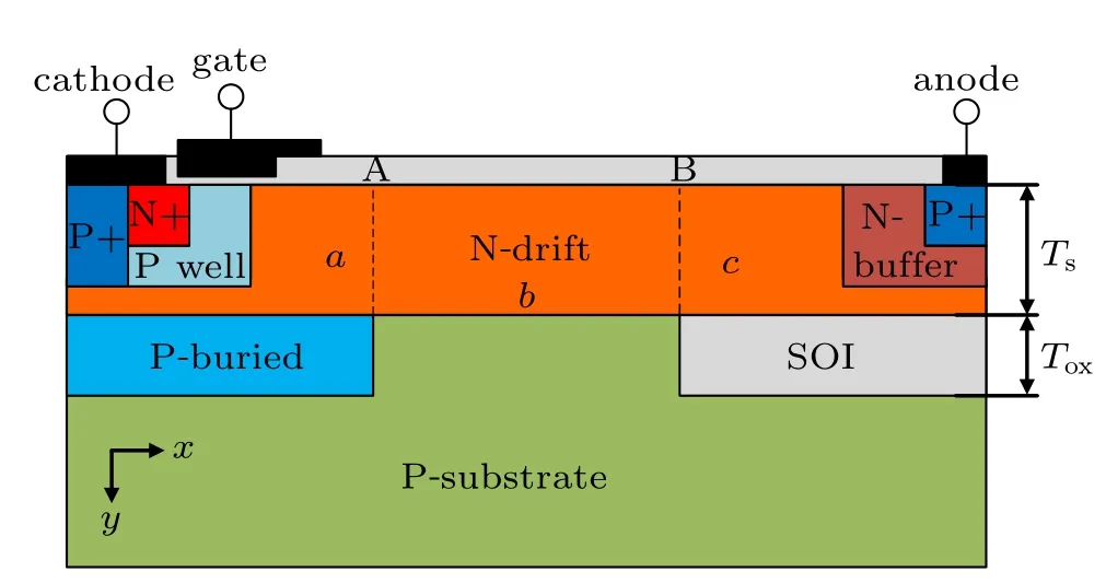
Fig.1. The schematic cross-section of the proposed BPSOI LIGBT.
3. Results and discussion
Table 1 is the proposed device,conventional PSOI LIGBT and traditional SOI LIGBT simulation parameters. Figure 2 shows the lateral electric field distribution of the three structures. It can be clearly seen that the surface electric field of the BPSOI LIGBT structure has two peaks(near A and B)under the action of the additional electric field generated by the Ptype buried layer charge,which raise the bottom of the electric field and reduces the peak value of the electric field at both ends of the source and drain. Compared with the traditional SOI LIGBT and conventional PSOI LIGBT,electric field distribution of the proposed device is more uniform. The position of the peak is located at the interface between different types of substrates,which improves the lateral withstand voltage of the device.
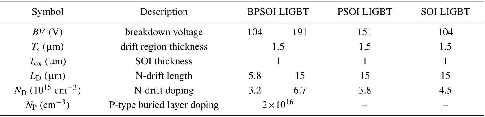
Table 1. Device design parameters.
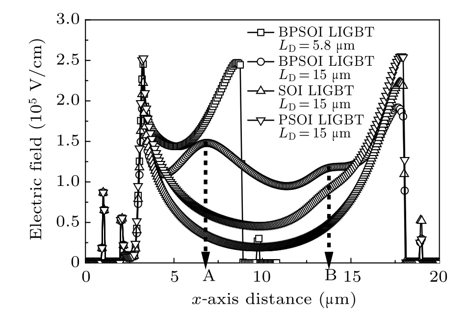
Fig.2. Lateral electric field distribution of the BPSOI LIGBT,conventional PSOI LIGBT,and traditional SOI LIGBT.
Figure 3(a)compares the lateral surface potential distribution of the proposed structure with the traditional SOI LIGBT at breakdown. It can be seen that when LD= 5.8 µm, the proposed BPSOI LIGBT can obtain almost the same breakdown voltage (BV = 104 V) as the traditional SOI LIGBT(LD=15 µm), the proposed device makes the device have a smaller size. When LD=15µm,the proposed BPSOI LIGBT obtains a BV of 191 V. It can be concluded that at the same LD, the breakdown voltage of the proposed BPSOI LIGBT is increased by 84%,compared with the traditional SOI LIGBT.This proves that the P-type buried layer and the partial-SOI layer introduced in the proposed device optimizes the surface electric field distribution, makes the electric field distribution more uniform,and obtains a higher breakdown voltage.Therefore, the BPSOI LIGBT obtains narrower LDand higher BV through electric field modulation.
Figure 3(b)shows the vertical potential distribution at the drain end of three structures, where 0 <y <W is the potential distribution of the device drift region and the buried layer,y>W is the potential distribution of the substrate. The substrate bears a considerable part of the vertical voltage,which is the reason of the BPSOI LIGBT structure has higher withstand voltage than the conventional SOI structure. Lines 1 and 2 indicate the potential difference between the drift area and the buried layer of the conventional PSOI LIGBT and the BPSOI LIGBT.It can be seen that the potential difference between the two structures in this part is similar. However,in the substrate part,the proposed BPSOI LIGBT has a more obvious potential than the conventional PSOI LIGBT.The increase is due to the optimization of the surface electric field by the P buried layer of the BPSOI LIGBT (as shown in Fig.2). In this way, the proposed BPSOI LIGBT improves the lateral withstand voltage by optimizing the surface electric field.

Fig.3. (a) Lateral surface potential distribution of the proposed structure and traditional SOI IGBT at breakdown. (b)Vertical potential distribution of the drain ends of BPSOI LIGBT, PSOI LIGBT, and SOI LIGBT,point W at y=2.5µm.
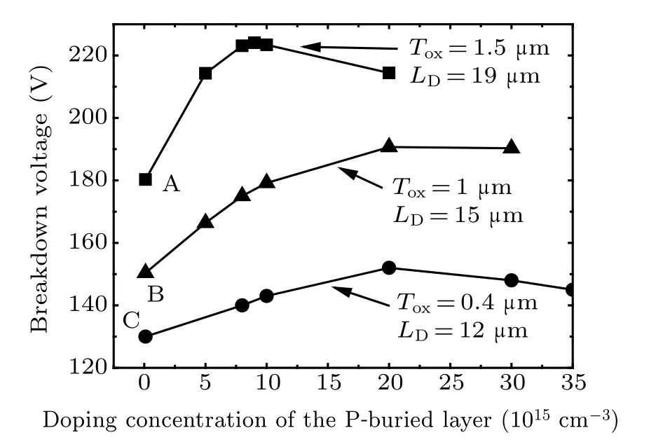
Fig.4. Relationship between the doping concentration of the P-type buried layer and breakdown voltage of the BPSOI LIGBT.
Figure 4 shows the relationship between the concentration of the P-type buried layer and breakdown voltage of the BPSOI LIGBT. Point A, point B, and point C on the dotted line represent the situation when NP=1×1014cm−3, which are the breakdown voltage of the conventional PSOI LIGBT.It can be seen from the figure that as NPincreases, the effect of the buried layer on the drift region gradually increases,and the surface electric field gradually tends to optimize.The highest peak of the electric field distribution on both sides gradually decreases,and the middle part gradually increases,which makes the breakdown voltage increase gradually. When NPoptimizes the electric field as shown in Fig.2,the breakdown voltage reaches the maximum.At this time,increasing NPwill cause the peak value of the electric field near the source end to be too high,thereby reducing the breakdown voltage. It can be seen from Fig.4 that the breakdown voltage of the BPSOI structure is increased by 26% compared to the conventional PSOI LIGBT.
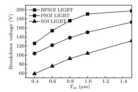
Fig.5. Relationship between the thickness of buried layer and breakdown voltage.
Figure 5 shows the relationship between the thickness of buried layer (Tox) and breakdown voltage of three different devices. As seen from the figure, with the increase in the thickness of the buried layer, the breakdown voltage shows approximately linear growth. The breakdown voltage of the proposed structure is higher than that of conventional PSOI LIGBT and traditional SOI LIGBT, because of the introduction of P-type buried layer to modulate the surface electric field. Among the structural parameters with LD= 15 µm,Ts=1.5µm,NP=2×1016cm−3.

Fig.6.Simulated forward characteristics of the proposed and traditional SOI LIGBT.
Figure 6 shows the simulated forward characteristics of the proposed structure (LD= 5.8 µm, Tox= 1 µm, NP=2×1016cm−3, BV = 104 V) and traditional SOI LIGBT(LD=15µm,Tox=1µm,BV =104 V).The proposed device has a shorter LD, and the electrically neutral effect of the Ptype buried layer in the structure increases the optimized concentration of the drift region,so the proposed device has better current capability. The BPSOI LIGBT gains the lower VFof 1.31 V at ICE=1.0 kA/cm2as shown in Fig.6,the curve representing BPSOI LIGBT in the figure is above the traditional SOI LIGBT, and the analysis and simulation results are consistent. The BPSOI LIGBT has good forward characteristics.
Figure 7 shows the simulated resistive load turn-off characteristics of the proposed structure(LD=5.8µm)and traditional SOI LIGBT (LD=15 µm). The BPSOI LIGBT gains the lower VFof 1.31 V at ICE=1.0 kA/cm2,when T =300 K and VG=10 V,the turn-off BPSOI LIGBT is 15.8 ns and that of SOI LIGBT is 37.5 ns. It can be clearly seen that the turnoff time of BPSOI LIGBT is less than the turn-off time of traditional SOI LIGBT. Due to the electric field modulation effect,the proposed structure has a smaller LD,so that the drift region obtains less storage carriers, and at the same time, the small LDdepletes the drift region quickly and obtains a shorter depletion region length.The shorter length of the depletion region and the smaller number of storage carriers are more conducive to device turn-off. Therefore, the proposed structure has a smaller Toffthan the traditional SOI LIGBT.
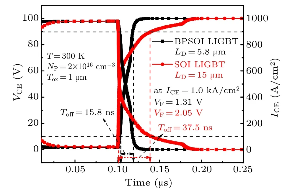
Fig.7. Simulated resistive load turn-off characteristics of the proposed BPSOI LIGBT and traditional SOI LIGBT.T =300 K,VG=10 V.
Figure 8 compares the tradeoff curves between forward voltage drop and turn off time for the BPSOI LIGBT and the conventional SOI LIGBT. The Toff~VFcurve is obtained by changing the anode P-type doping concentration at T =300 K and current density of 1 kA/cm2. The BPSOI LIGBT curve is below the traditional SOI LIGBT curve,indicating that the proposed structure has a better compromise between Toffand VF. When VF=2.05 V, the Toffof the proposed structure is 71% lower than that of the traditional SOI LIGBT. The proposed structure has low power consumption.
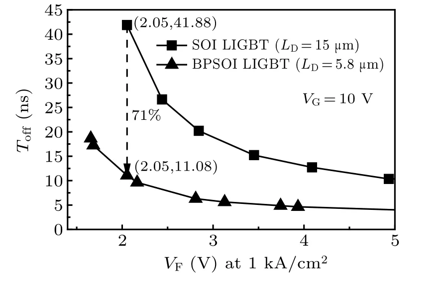
Fig.8. Tradeoff curves between forward voltage drop(VF)and turn off time(Toff)for the BPSOI LIGBT and the conventional SOI LIGBT.
The influence of the self-heating effect of the traditional SOI LIGBT is obvious. The self-heating effect seriously affects the reliability of the device, adversely affects the normal operation of the device,and degrades the performance of the device. However, the proposed device has a silicon window and retains the characteristics of the general PSOI LIGBT,the proposed device structure has better heat dissipation performance and alleviates the self-heating effect brought by the SOI structure. Figure 9(a)shows the temperature distribution inside BPSOI LIGBT and SOI LIGBT,and figure 9(b)shows the surface temperature of the two structures. The gate voltage VG=5 V,drain voltage VD=10 V.It can be clearly seen that the working temperature of the proposed BPSOI LIGBT is much lower than that of the SOI LIGBT.The BPSOI LIGBT reduces the heating of the device caused by the self-heating effect.
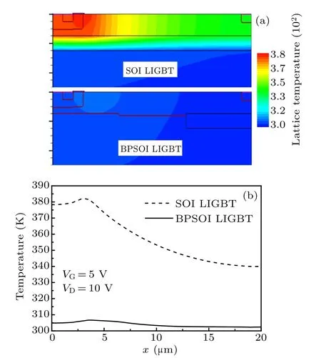
Fig.9. (a)Temperature distribution inside BPSOI LIGBT and SOI LIGBT.(b)Surface temperature of the two structures.
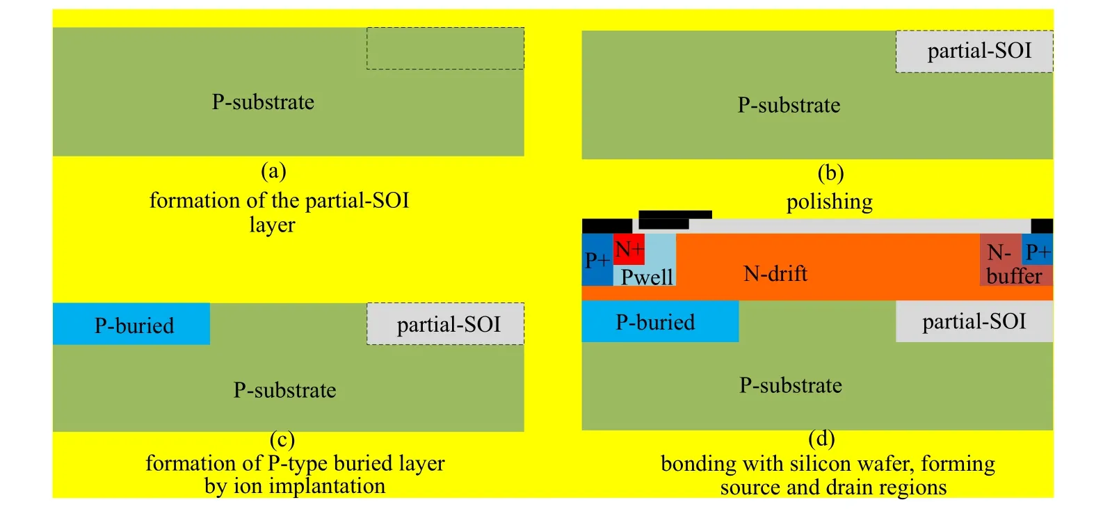
Fig.10. Key process flow of the proposed BPSOI LIGBT.
In engineering, the BPSOI structure can be realized by silicon wafer direct bonding(SDB),as shown in Fig.10. The difference from the general PSOI structure in the SDB process is that it adds a P-type ion implantation step. First, a part of the buried oxide layer is formed,and at the same time a part of the silicon window of the device is formed, and then etching and chemical polishing techniques are used to etch and polish the oxide layer on the silicon surface. In the third step,ion implantation is performed,and the implanted ions form a part of the p-type buried layer.Finally,it is directly bonded to another silicon wafer without an oxide layer.
4. Conclusion
A novel SOI LIGBT with BPSOI structure has been proposed in this paper. Simulation and analysis verified that the proposed BPSOI LIGBT has the advantages of optimizing the surface electric field and alleviating the self-heating effect.The electric field modulation of the P-type buried layer and a partial-SOI layer charge results in tow peaks in the surface electric field, the electric field is more uniformly distributed than the traditional SOI LIGBT,so that the device has a larger BV.Thus,shorter drift region and lower storage carrier are obtained. Compared with traditional SOI LIGBT, the proposed structure has better tradeoff between Toffand VF.
猜你喜欢
——宝兴鹛雀
杂志排行
Chinese Physics B的其它文章
- Statistical potentials for 3D structure evaluation:From proteins to RNAs∗
- Identification of denatured and normal biological tissues based on compressed sensing and refined composite multi-scale fuzzy entropy during high intensity focused ultrasound treatment∗
- Folding nucleus and unfolding dynamics of protein 2GB1∗
- Quantitative coherence analysis of dual phase grating x-ray interferometry with source grating∗
- An electromagnetic view of relay time in propagation of neural signals∗
- Negative photoconductivity in low-dimensional materials∗