Broadband absorption enhancement with ultrathin MoS2 film in the visible regime∗
2021-03-11JunWu吴俊
Jun Wu(吴俊)
1College of Electrical Engineering,Anhui Polytechnic University,Wuhu 241000,China
2Department of Physics,Zhejiang University of Science and Technology,Hangzhou 310023,China
Keywords: two-dimensional (2D) materials, transition-metal dichalcogenide, plasmonics, absorption enhancement
1. Introduction
Recently, two-dimensional (2D) materials such as graphene and transition-metal dichalcogenide(TMD)have attracted tremendous research interests owing to their unique optical, electrical, and mechanical properties.[1–3]Following the success of graphene,TMD materials,such as MoS2,WS2,MoSe2, and WSe2, have emerged as a new class of semiconductors that exhibit distinctive properties at monolayer thickness.[4–6]One of the most appealing features of TMD materials is to enable the development of novel optoelectronic and photovoltaic devices with an atomic-scale dimension owing to their semiconducting nature and strong excitonic properties.[7–12]However, the single-pass absorption of monolayer TMD materials is usually lower than 10% within the visible wavelength.[13,14]While it is remarkably high in consideration of their single atomic thickness,it is insufficient for high performance devices when applied in the field of solar cells and photodetectors,standing as a major challenge for device development. Moreover,for photovoltaic device applications,broadband enhancement of absorption over the entire wavelength range above the band gap is highly desirable.
Under these circumstances, to realize true 2D optoelectronic and photovoltaic devices, efforts toward enhancing light–matter interactions and boosting absorption in 2D TMD materials should be made. In order to address this challenge,many configurations based on different physical mechanisms have been proposed and demonstrated. Piper et al.demonstrated broadband absorption enhancement in monolayer MoS2placed on a photonic crystal slab backed by a perfect electric conductor mirror,where an average absorption of 51%at normal incidence is achieved due to the guided mode resonances effect.[15]Bahauddin et al.proposed a simple plasmonic architecture, MoS2/Ag nanoparticles/NiOx/Al, which can achieve broadband absorption of 35%within a monolayer MoS2.[16]Huang et al. proposed to combine MoS2film with resonant photonic structures,which enables strong absorption(>70%)in MoS2film(≤4 layers)for either narrowband incidence or broadband incidence like solar radiation.[17]Jariwala et al. proposed an ultrathin, near-unity, broadband absorber using TMD/metal heterostructure and applied in Schottky junction devices.[18]Long et al.have employed silver grating to boost the absorption in monolayer MoS2,which is based on the excitation of multi-order magnetic polaritons.[19]Butun et al. demonstrated absorption enhancement in WS2/Ag nanodisks heterostructures due to electric field localization in the vicinity of Ag nanodisks.[20]Zhang et al. proposed a broadband absorber made of MoS2film,which is polarizationinsensitive, and the absorption peak maintains a high value over a large incident angle range for both polarizations.[21]Wong et al. reported experimental measurements for ultrathin (<15 nm) van der Waals heterostructures, which exhibits external quantum efficiencies above 50%.[22]Kim et al. demonstrated that the phase changes at MoS2interfaces enabled absorption enhancement of monolayer MoS2on sub-100 nm thick SiO2/Si substrates.[23]Wang et al. reported a modified-MoS2-based Tamm plasmonic structure where the perfect absorption can be achieved in the visible range.[24]Qi et al. demonstrated that dual-band absorption enhancement could be achieved in monolayer MoS2by a tapered metamaterial waveguide slab.[25]Though schemes mentioned above have demonstrated absorption enhancement in TMD materials, they still fall short of providing sufficient absorption enhancement,especially for broadband incidence like solar radiation.
In this work, the broadband light trapping effect of absorber based on MoS2film is investigated. First, the geometric parameters of the proposed absorber are obtained by employing the rigorous coupled-wave analysis(RCWA)[26,27]and the simulated annealing algorithm.[28,29]The absorption spectra under normal incidence are calculated and compared with those of an optimized planar reference structure with the equal thickness of MoS2film. Then the optical properties,including the integrated absorption, the short-circuit current density, and their angular independence, are calculated and investigated. Last, the electromagnetic field distributions at some selected wavelengths are illustrated to provide a qualitative explanation of such broadband absorption enhancement effect.
2. Design and results
A thin MoS2film of thickness hmand refractive index nmis sandwiched between a SiO2film and a one-dimensional silver(Ag)grating backed with an Ag mirror,as shown in Fig.1.The grating is periodic in the x-direction and uniform in the y-direction. The grating is defined by the period d, the width w = fd (where f denotes the fill factor), and the thickness hAg, the ridge material Ag, and groove material SiO2. The thickness of the SiO2film is hs. The refractive index of SiO2is 1.45, while the refractive indices of Ag and MoS2in the visible regime are obtained from Refs. [30,31], respectively.The thickness of the MoS2film is selected as 13 nm, i.e.,hm=13 nm. And the thickness of the Ag mirror is fixed to be 100 nm to prevent the transmission of light. Transverse electric(TE,with the electric field along the y axis)and transverse magnetic(TM,with the magnetic field along the y axis)polarized plane waves are incident from the air with angle θ.
To provide a figure of merit(FOM),we employed the integrated absorption,which considered absorption at all wavelengths. The integrated absorption values for TM and TE polarizations can be described by[32,33]


where S(λ) is the solar irradiance spectrum, which is considered as the AM1.5g solar spectral intensity distribution.αTE(λ) [αTM(λ)] is the absorption spectra of TM (TE) polarized light calculated by RCWA, which is achieved by our home-made code(with the number of harmonics equal to 40).For the absorber in Fig.1, the wavelength-dependent absorption spectra are calculated by employing[34]

where ω is the angular frequency, ε0and ε denote the permittivity of vacuum and the relative permittivity of the active material,and E is the electric field. The integral is over a single period.

Fig.1. Schematic diagram of the proposed MoS2 absorber.
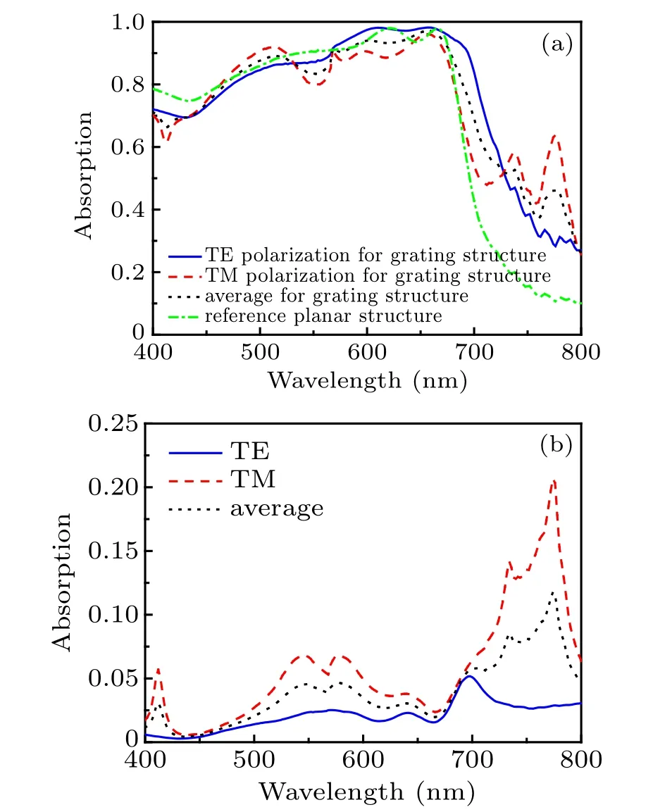
After numerical optimization, we obtain the geometric parameters of the proposed absorber, which is shown as follows: d =568 nm, f =0.79, thickness hAg=137 nm, hs=84 nm. Figure 2 shows the absorption spectra of the absorber for light under normal incidence. For comparison,a reference structure, where a thin MoS2film with a thickness of 13 nm sandwiched between a SiO2film with a thickness of 72 nm and an Ag mirror, is also calculated and shown in Fig.2. As can be seen from Fig.2(a), the absorption of the reference planar structure is greater than 70% at wavelengths of 400–686 nm, whereas it is low in the long wavebands. The low absorption in the long wavebands is attributed to the smaller extinction coefficient of MoS2at wavelengths of about 700–800 nm compared to that in the short wavebands. However,when the part of the Ag mirror is patterned with the periodically grating,the absorption in MoS2film is enhanced strongly in the long wavebands, which leads to broadband absorption for both polarizations. Though the absorption of the reference planar structure is higher than the grating structure in the short wavebands, the overall broadband absorption performance of the grating structure is superior to that of the planar structure,which can be demonstrated by examining the integrated absorption. Under normal incidence, the average integrated absorption is 77.77%for the grating structure and 72.75%for the planar structure. Therefore, the absorber with the bottom Ag grating structure exhibits an integrated absorption enhancement of about 7%compared to the planar structure.
Due to the intrinsic feature of metal, the Ag grating and mirror can also absorb the incident light, which is undesirable and should be minimized during the process of design.In Fig.2(b),we show the absorption spectra in Ag grating and mirror. It is found that the absorption in Ag for TM polarization is higher than that of TE polarization in nearly the entire waveband range. In general, the average absorption in Ag is low in the short waveband and increases when the wavelength is above 700 nm.

Fig.2. The simulated absorption as a function of wavelength for light absorption in(a)MoS2 and(b)Ag grating and Ag mirror.
3. Discussion
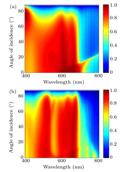
For the analysis above,the absorption properties are considered only for light under normal incidence. However,for practical application, the broadband absorption should be maintained over a wide range of incident angles. Under this circumstance,we calculate the absorption spectra as functions of the wavelength and incident angle for both TE and TM polarizations, which are shown in Figs. 3(a) and 3(b), respectively. For TE polarization,the absorption remains above 80%in the wavelength range of 560–666 nm with incident angle up to 60◦. And the absorption is low in the long wavebands over the entire incident angle range.While for TM polarization,the absorption can remain above 80%at the incident angle of 60◦in the wavelength ranges of 492–538 nm and 580–680 nm. In addition, the absorption also exhibits a decrease in the long wavebands with the increase of incident angle. The angle insensitivity in the short wavebands for both polarizations can be explained as follows. In the short wavebands,the refractive indices of MoS2are large, which results in an enormous refractive index contrast between the air and the MoS2. With the increase of incident angle in air, the change of incident angle in the MoS2is very slow, which leads to the large angle insensitivity. In general,the broadband absorption enhancement for both polarizations can be maintained over a wide range of incident angles,which exhibits large angle insensitivity.

Fig.3. Simulated absorption spectra as functions of the wavelength and angle of incidence for(a)TE and(b)TM polarization.

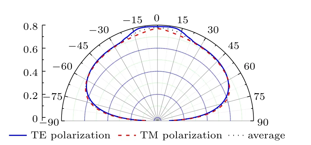
Fig.4. Integrated absorption (TM, TE, and average) as a function of incident angle for the proposed absorber.
To intuitively confirm the angle insensitivity,we show the simulated integrated absorptions for both polarizations as a function of incident angle in Fig.4, where the averaged integrated absorption denotes the mean of the values of TE-and TM-polarized light. For TE-polarized light,the integrated absorption remains above 60% (70%) for the incident angle up to 70◦(49◦),while it is higher than 60%(70%)over an angle range of 0◦to 72◦(0◦to 43◦) for TM-polarized light. In addition, the integrated absorption for TE polarization is larger than that for TM polarization when the incident angle is less than 59◦, whereas the situation is opposite when the angle is larger than 59◦, indicating that the angle insensitivity of TEpolarized is better than that of TM-polarized light. In general,the averaged integrated absorption still maintains a value higher than 60%(70%)for the incident angle up to 71◦(47◦),indicating large angle insensitivity,which is especially attractive for real applications.
For application in the field of the solar cell, the shortcircuit current density Jsc(mA/cm2) is usually considered,which can be defined as follows:[35,36]

where the internal quantum efficiency is assumed to be 1, λ is the wavelength, q is the elementary charge,h is the Planck constant, and c is the speed of light; the integration is from λmin=400 nm to λmax=800 nm,i.e.,the visible light region.To examine the potential for photovoltaic applications, we show the short-circuit current density versus the angle of incidence in Fig.5.It is found that the short-circuit current density of TE polarization remains above 17 mA/cm2(15 mA/cm2)for incident angle up to 54◦(69◦), whereas it still maintains a value higher than 17 mA/cm2(15 mA/cm2) when the incident angle is less than 55◦(72◦) for TM polarization. Note that the Jscvalue for TE-polarized light exceeds that for TMpolarized light with the incident angle in the ranges of 0–26◦and 33◦–51◦, whereas the opposite is true for other incident angles. In general, the averaged short-circuit current density remains above 17 mA/cm2(15 mA/cm2) for incident angle up to 55◦(70◦),which exhibits slowly decrease with increasing incident angle. Therefore, the Jscvalue of the proposed absorber possesses large angle insensitivity, which presents a promising potential for solar energy trapping.

Fig.5. Short-circuit current density Jsc (TM, TE, and average) as a function of incident angle for the proposed absorber. The averaged Jsc value is defined as the mean of the values for TE-and TM-polarized light.

Fig.6. Electric field distribution for TE polarization at the wavelength of (a) 400 nm and (b) 658 nm; magnetic field distribution for TM polarization at the wavelength of(c)514 nm and(d)776 nm. The origin of the z-axis is located at the bottom of the Ag mirror.
In order to give a qualitative understanding of such broadband absorption enhancement effect,the electromagnetic field distributions at some selected wavelengths are illustrated in Fig.6. For TE polarization, we select the short wavelength(400 nm)and the resonant wavelength with maximum absorption(658 nm),which are shown in Figs.6(a)and 6(b),respectively,whereas the resonant wavelengths of 514 nm(Fig.6(c))and 776 nm (Fig.6(d)) are selected for TM polarization. As shown in Figs. 6(a) and 6(b), there are strongly electric field intensity enhancement and concentration in the dielectric film,MoS2film, and grating grooves. Moreover, the electric field intensity distributions exhibit clear standing wave profiles in the x-direction,which is a typical feature of a leaky mode.The enhanced absorption in MoS2film for TE polarization can be attributed to the excitation of leaky mode resonance.However,for TM polarization, the magnetic field intensity is enhanced at the interface between Ag grating and MoS2film and the interface between the grating ridge and grating groove at the wavelength of 514 nm, while it is enhanced only at the interface between Ag grating and MoS2film at the wavelength of 776 nm. Both distributions exhibit a typical feature of surface plasmon resonance. Therefore, the enhanced absorption in MoS2film for TM polarization can be attributed to the excitation of plasmon resonance at the surface of Ag grating.
4. Conclusion
In summary, a broadband absorber based on ultrathin MoS2films is proposed and investigated. It consists of a MoS2film sandwiched between a dielectric film and a onedimensional silver grating backed with a silver mirror. The broadband absorption enhancement for both polarizations in the visible region is achieved, which exhibits large integrated absorption and short-circuit current density for solar energy under normal incidence. The optical properties of the proposed absorber are found to be superior to those of a reference planar structure,which makes the proposed structure attractive for solar energy trapping application. More importantly, the integrated absorption and short-circuit current density of the proposed absorber possesses large angle insensitivity, which is particularly useful for photovoltaic applications. A qualitative understanding of such broadband absorption enhancement effect is examined by illustrating the electromagnetic field distribution at some selected wavelengths. It is believed the results will enable the development of high-performance optoelectronic devices,such as solar cells,photodetectors,and modulators.
杂志排行
Chinese Physics B的其它文章
- Novel traveling wave solutions and stability analysis of perturbed Kaup–Newell Schr¨odinger dynamical model and its applications∗
- A local refinement purely meshless scheme for time fractional nonlinear Schr¨odinger equation in irregular geometry region∗
- Coherent-driving-assisted quantum speedup in Markovian channels∗
- Quantifying entanglement in terms of an operational way∗
- Tunable ponderomotive squeezing in an optomechanical system with two coupled resonators∗
- State transfer on two-fold Cayley trees via quantum walks∗
