Nanoimprinted structures for organic light-emitting devices and lasers
2021-03-11130012
( , , , 130012,)
Abstract:Organic light-emitting devices (OLEDs) have been developed and applied rapidly in the past three decades as both display and lighting panels due to their advantages.However,inherent low light extraction efficiency always makes them require to integrating the light extraction micro/nano structures.On the other hand,organic semiconductor laser (OSL) also has attracted much attention due to the advantages of wide emission spectrum,simple fabrication,low cost and easy integration.Also,micro/nano structures should be fabricated in the OSL as resonator geometries for optical feedback to achieve lasing action.Among the different fabrication techniques,nanoimprint lithography (NIL) as a patterning process with high-resolution,high-throughput and cost effective,is considered to be one of the most promising technologies.NIL not only can break the limitation from diffraction limit and beam scattering,but also guarantee the inherent optical and electronic properties of organic optoelectronic materials.Here,we summarize and evaluate the fabrication of nanostructured electrode,functional layers and encapsulation films in the OLEDs and nanostructured dye-doped polymer and luminescent materials in the OSLs.
Key words:nanoimprint lithography;organic light-emitting devices;organic semiconductor laser
1 Introduction
Organic light-emitting devices (OLEDs)[1-4]and organic semiconductor lasers (OSLs)[5-7]based on organic semiconducting materials have been considered as potential and promising candidates in optoelectronics.One reason is the inherent advantages of organic materials including wide materials sources,cost effective,compatibility with roll to roll process and flexibility[8-10].Another is the efficiency and lifetime of organic optoelectronic devices continuous rapid improvement[11-12].According to the abovementioned advantages,organic light source devices lead to a great many significant commercial applications.For instance,OLEDs have been already used in panel display including the smart phone and television widely[13-15].OSLs is considered as the potential alternative light source of integrated photonic chip[16-17].
Since the pioneering reports,a wide variety of research on OLEDs and OSLs have been conducted in both academia and industries.The research involves the field of material synthesis,fabrication process and structure design etc.Also,a great many review articles on different perspectives of OLEDs and OSLs have been reported[18-20].In this review,we focus on the nanoimprinted structures for OLEDs and OSLs to supply a complementary perspective since nanostructures have been proved the value and significance on improving the performance of the devices,and nanoimprint lithography has been also demonstrated high-resolution,high-throughput and cost effective.Different from traditional high resolution lithographic technologies including ultraviolet (UV) lithography,E-beam lithography[21]etc.,which fabricate nano-pattern using photons or electrons to modify the chemical cross linking of the resist,NIL achieve the pattern based on mechanical deformation at the fluidic or elastic state.Consequently,NIL not only could break the limitation from diffraction limit and beam scattering,but also guarantee the inherent optic and electronic properties of organic optoelectronic materials.Therefore,NIL has been considered as the promising technology to integrate the nanostructures into organic optoelectr-onic devices in commercial application.
The nanoimprint process is proposed by Chou et al.in 1995[22].The process is simple,a silicon (Si) wafer with silica nanostructured surface as a mold is pressed on a polymethylmethacrylate (PMMA) film on the Si substrate,which has been heated and the temperature should be higher than its glass transition temperature but lower than the melting temperature.In this condition,PMMA film behaves as a viscoelastic state and replicates the nanostructures of the mold conformally.During the nanoimprinting,the condition in terms of temperature,pressure and duration time should be adjusted to realize optimal nanostructures.After cooling down below glass transition temperature,the PMMA film will return to solid state.Finally,the nanostructure could be obtained after the mold removes from Si substrate.It is obvious that the mold with nanostructures and the target materials are the fundamental elements for NIL from abovementioned technical process.This review will pay more attention to the pattern of target materials because the performance of devices is not relatively dependent on mold fabrication process.We will summarize the extensive studies on OLEDs and OSLs with NIL in detail as follow.
2 NIL for OLEDs
OLEDs have been already exhibiting excellent commercial application in panel display including smart phone and television widely,as well as in solid state light sources[23-26].And a great many academic research have been proved that micro/nano structures have ability to improve the light extraction of OLEDs[27-33].After the NIL reported,Chou et al.introduced NIL into organic materials since integrating the micro/nano structures is effective to manipulate the light in the organic optoelectronic devices[34].Both small molecule and polymer submicron structures have been demonstrated using NIL in their research.Fig.1 (a,b) show atomic force microscope (AFM) images of DCMII doped in Alq3grating,and Fig.1(c) shows SEM image of the polymer PMMA with Alq3/DCMII.The periods are 200 nm,300 nm and 200 nm respectively,which reveal high enough resolution to apply into the visible light region.It is worth noting that the optical and electronic properties of organic materials whether or not suffer from degradation due to the temperature and pressure during the nanoimprint process,or demolding process after the nanoimprint.Fig.1(d) reveals no degradation occurred because of almost identical photoluminescence curves before and after nanoimprint.Although just nanoimprinted organic thin film rather than devices was demonstrated,it is a pioneering investigation of nanoimprint technology on organic optoelectronics.In this section,OLEDs with nanoimprinted structures will be focused.Generally,nanoimprinted structures in OLED are classified internal and external light extraction.The internal light extraction refers to surface plasmon-polaritons (SPPs) mode (electromagnetic waves caused by coupling between photon and electron,located along the metallic electrode/organic interface) and waveguide (WG) mode (in ITO and organic layer due to their high refraction index),while the external light extraction refers to substrate mode (total internal reflection at the substrate/air interface).Fig.2(a) illustrates light emission mode of a conventional bottom-emitting OLED[35].The light trapped in ITO,substrate and the interface of Alq3/Al corresponding to WG mode,substrate mode and SPPs mode in the planar device.Conversely,the trapping mode could be extracted by the internal and external nanostructures as shown in the Fig.2(b).In regard to extraction mechanism,Feng et al have discussed in detail in their review[18].On one hand,an appropriate periodicity such that waveguided light is Bragg-scattered into the forward direction is required for the periodic micro/nano patterns by satisfying the Bragg scattering condition.

Fig.1 Origin of nanoimprint lithography with organic materials.(a,b) AFM images of the Alq3 /DCMII;(c) SEM image of the grating of PMMA/Alq3 /DCMII;(d) Luminescence spectral intensity before and after nanoimprint.Reprinted with permission of Ref.[34],Copyright 1999 American Institute of Physics.
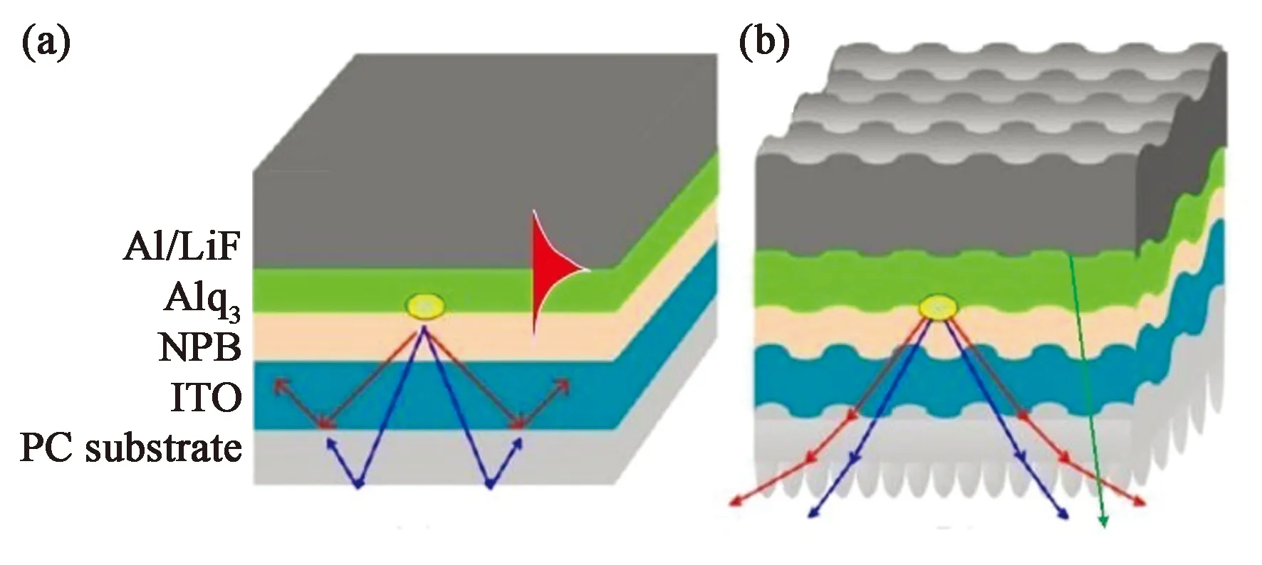
Fig.2 Schematic diagram of light emission modes and extraction strategies of a conventional bottom-emitting OLED.(a) Structures and light propagation illustration of OLED;(b) Schematic explanation of the mechanism for improving device out-coupling efficiency with nanostructures (The green arrow corresponds to the SPPs mode,the red arrow corresponds to the waveguide mode,and the blue arrow corresponds to the substrate mode).Reprinted with permission of Ref.[35],Copyright 2014 American Chemical Society.
2dsinθ=nλ,
(1)
where,drepresents the period of nanostructure,θis the emission angle,λis the wavelength of the emitted light.andnis an integer.On the other hand,SPPs power losses also can be coupled out by manipulating the propagation of photons in OLEDs and providing an additional momentum to couple the SPP modes into light.
(2)
where,kSPPis the in-plane wavevector of the SPP,klightis the wavevector of the emitted light,Λis the period of the corrugation,αis the emission angle,andmis an integer.Here,we would like to introduce the integrating nanostructures into OLEDs by NIL.
2.1 Nanostructured electrode
Considerations for fabricating process and the extraction of light,the nanostructured electrode came into sight firstly,since the electrodes generally have better stability and machinability compared to organic layers in the OLEDs and there is about 40% SPPs loss in the interface between the metal electrode and organic layer[36].As a matter of fact,most nanostructured electrodes fabricated by NIL were reported that evaporating the electrode on the imprinted substrates[37-38].Despite of the increased luminance and efficiency of OLEDs,the evaporated nanostructured electrode ran into compromised surface morphology and continuity.Recently,the nanostructure directly imprinted on electrode has been demonstrated in our work[39].As shown in Fig.3(a),different from imprinting the nanostructure on the target materials without electrode,we imprinted an ultrathin metal film directly by polymer (SU-8)-assisted thermal nanoimprint.The ultrathin metal film was evaporated on an uncured photopolymer,which not only used as a seed layer to improve the continuity and conduction of metal film but also as an assisted layer for imprinting.Due to the elasticity and viscidity of the uncured polymer film,the metal film would corrugate conformally with underneath polymer during the nanoimprinting process.Compared to as-evaporated on the corrugated nanostructures,the ultrathin metal film showed better smoothness by eliminating the adverse effect originated from the fluctuation of the underneath nanostructures during the electrode deposition.Fig.3(b~e) illustrated the surface morphologies of the ultrathin metal film with different fabrication process.Both corrugated nanostructures show good regularity with period of 320 nm and depth of 60 nm.However,the surface morphology of imprinted Au/SU-8 film has been improved and the roughness has been decreased obviously as shown in the AFM figures.This improvement originated from eliminating the inhomogeneous evaporation which caused by the differences nucleation and growth on the facet,edge and corner of the corrugated nanostructures.Moreover,this improvement is benefit to the performance of OLED fabricated with the nanoimprinted electrode.

Fig.3 Nanostructured electrode fabrication by NIL.(a) Schematic of the fabrication process.SEM (b) and AFM (d) images of Au (7 nm)/Ag (1 nm) composite grating film fabricated through imprinting SU-8;SEM (c) and AFM (e) images of Au (7 nm)/Ag (1 nm) composite grating film fabricated through imprinting Au.The insets in (d) and (e) show the enlarged area of the corrugated metallic films.Reprinted with permission of Ref.[39],Copyright 2019 IEEE.
2.2 Nanostructured functional layers
In condition of OLEDs with transparent nonmetallic bottom electrode,there is none of SPPs loss at the interface between bottom electrode and organic layer.The nanostructures have no more need of integrating to bottom electrode,such as ITO,graphene and silver nanowires (AgNWs).Therefore,in order to avoid the SPPs loss of OLEDs at the top interface between top electrode and organic layer,nanoimprint has been conducted in the organic layer or inorganic buffer layer.Taking account into the proper elasticity and viscidity,thin films prepared by solution process have been selected firstly reported by Prof.Tang et al.The most commonly used is PEDOT∶PSS film.Fig.4(a) shows the AFM figure of the nanoimprinted PEDOT∶PSS film,a continuous tapered pattern with secondary sub-wavelength structures was displayed[40].The average depth of tapered cone is about 70 nm,which not only ensure the sequential deposition of organic layers and metal electrode on the patterned PEDOT∶PSS layer duplicating the nano-pattern conformally,but also is beneficial to the suppression of possible anomalies in the current flow when the depth is too high.As a result,the light extraction of OLEDs fabricated with nanostructures could be enhanced as well as the regular carrier injection and transport.Also,a sol-gel derived ZnO layer was used as imprinted layer[41].It is obvious that the high quality nanocones array could be imprinted onto the ZnO layer (Fig.4(b)).It should be mentioned that thermal nanoimprint has replaced pressure nanoimprint on the PEDOT∶PSS owing to the heat stability of ZnO.In addition,there is a superior design different from other attempts in the both abovementioned work.Considering the requirement of full-color display and broadband white lighting,aperiodic nanostructures with long-range disorder and short-range order have been adopted on PEDOT∶PSS and ZnO to break out the limitation of response to specific emission wavelengths of periodic structures[42].On the other hand,the possibility of using the small-molecule hole transport layer as the imprinted layer to improve performance of OLEDs has been also demonstrated.It can be clearly seen that the nanostructures can be transferred successfully on the surface of N,N′-diphenyl-N,N′-bis(1-naphthyl)-(1,1′-biphenyl)-4,4′-diamine (NPB) layers from Poly (dimethylsiloxane) (PDMS) layer after the nano-imprinting process (Fig.5(a),5(b))[43].The NPB surface could maintain the periodicity of nanostructures but was slight rougher compared to the PDMS mold.However,it still has ability to outcoupling the SPPs photon energy loss and then enhancing the light extraction by the momentum compensation between the momenta of SPPs and photons.As shown in Fig.5(c,d),the luminance and efficiency of nanostructured OLEDs have been both improved.It is worthy noting that this strategy still have much room for improvement because the height (a key factor of suppressing the SPPs loss) of NPB is obviously lower than the PDMS mold at present.
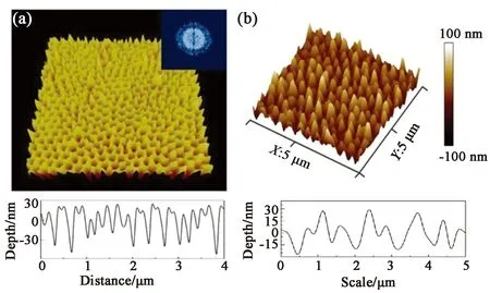
Fig.4 Nanostructured functional layers fabrication by NIL.(a) Perspective view of deterministic aperiodic nanostructures transferred to PEDOT∶PSS layer on ITO surface.Dimensions:4 μm×4 μm.The panels below indicate the depth profiles,showing the surface root-mean-square (RMS) roughness of about 6.5 nm.Insets show the fast Fourier transform (FFT) patterns of each image.(b) AFM topography morphologies and depth profiles for patterned ZnO on AgNWs.Reprinted with permission of Ref.[40],Copyright 2014 WILEY-VCH Verlag GmbH &Co.KGaA,Weinheim and Ref.[42],Copyright 2019 WILEY-VCH Verlag GmbH &Co.KGaA,Weinheim,respectively.
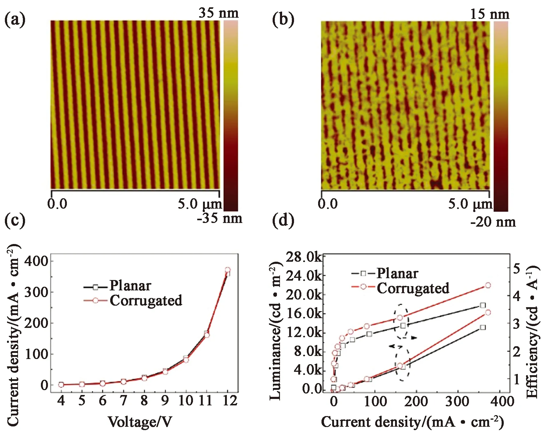
Fig.5 OLED efficiency enhancement with nano-structured functional layers fabricated by NIL.AFM images of nanostructures in (a) PDMS and (b) NPB.(c) Current density-voltage and (d) luminance-current density-efficiency characteristics of planar and corrugated OLEDs.Reprinted with permission of Ref.[43],Copyright 2016 Author(s).
2.3 Nanostructured encapsulation film
Due to the sensitivity of organic molecules to oxygen and water vapor,the development of encapsulation technology has been recognized as the key technology to achieve commercial OLEDs[44-45].Currently,the commonly adopted strategy is to encapsulate with the glass or polymer films[46-47].But there is a problem to be solved that light has to emit through the encapsulation layer,and total reflection at the interface between the encapsulation film and the air will give rise to power loss similar to substrate mode loss.In our previous work,we have proved that soft nanoimprinting is a high quality,low cost,high repeatable and highly effective strategy to integrate nanostructures onto the surface of the flexible polymer encapsulation films[48].Fig.6(a) shows a schematic diagram of introducing the nanostructure into the encapsulation films.The PDMS mold with the expected nanostructure is imprinted on the uncured NOA-63 encapsulation film and consequently exposure under a UV light source.The nanostructured encapsulation film could be fabricated after peeling off the PDMS mold.As shown in the AFM figure (Fig.6(b)),a tapered nanopillars array with good morphology and uniform periodicity can be obtained on the encapsulation film.This periodic tapered pillars array causes a refractive index gradient,therefore enlarge the critical angle of total reflection.As a result,the power loss at the surface between encapsulation film and air could be extracted effectively.As shown in Fig.6(c,d),the luminance and current efficiency are observably improved after employing the nanostructured.In addition,the nanostructured surface also could lead to a high contact angle,which is beneficial to prevent OLEDs from being polluted by reducing the probability of water condensation and dust accumulation.
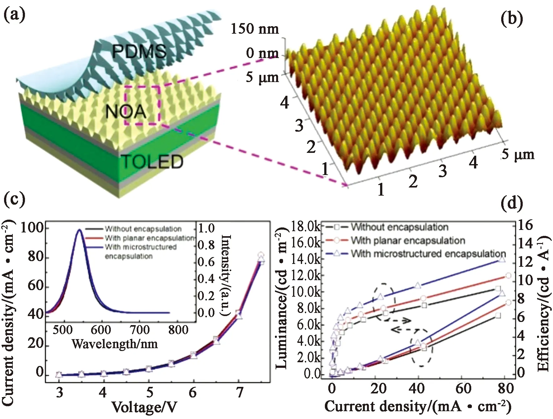
Fig.6 OLED efficiency enhancement with nanostructured encapsulation film fabrication by NIL.(a) Schematic process of TOLEDs with nanostructured encapsulation.(b) AFM figure of surface morphologies for the nanostructured encapsulation film.Current density-voltage (c) and luminance-current density-efficiency (d) curves of the TOLEDs with and without the encapsulation.Inset in (c):EL spectra of the TOLEDs with and without the encapsulation.Reprinted with permission of Ref.[48],Copyright 2014 Elsevier B.V.
3 NIL for OSLs
In addition to OLEDs,optically pumped organic semiconductor laser also has a great many development[49-52]on account of a wide range of applications as well as the advantages of wide emission spectrum,simple fabrication,low cost and easy integration[53-57].The simple and efficient nanoimprint lithography has been proved as an effective technology in the organic laser construction process[58-59].In this section,we will focus on discussing the OSLs fabricated by NIL.
3.1 Nanoimprinted luminescent dye-doped polymer
In earlier research of organic laser,the polymer dye lasers are one of the most attractive area due to the simple fabrication and large tunable emission[60-61].The dye doped into printable polymer could integrate the capability of the high efficient emission of the dye and the excellent elasticity and plasticity of polymer.In the NIL process,a hard mold could be used to transfer nanostructures with high fidelity onto polymer.As shown in Fig.7,the ring grating nanostructures[62](rhodamine 640-doped PMMA) and two dimensional triangular lattice photonic crystals[63](Rhodamine 6G-doped mr-NIL 6000) both exhibit good morphologies and high resolution.It should be mentioned that abovementioned NIL are both thermal imprint process,the operating temperature should be higher than the glass transition temperature of target polymer.In this condition,the polymer becomes high elastic state and could flow into the space of the mold.

Fig.7 Nanoimprinted luminescent dye-doped polymer for OSL.(a) SEM images of the imprinted rhodamine 640-doped PMMA film;(b) SEM images of nanoimprinted triangular lattice photonic crystals in dye-doped mr-NIL 6000 printable polymer.Inset:(left) SEM top view of one silicon stamp and (right) zoom of a dye-doped nanoimprinted photonic crystals.Reprinted with permission of Ref.[62],Copyright 2007 American Institute of Physics and Ref.[63],Copyright 2013 American Institute of Physics,respectively.
3.2 Nanoimprinted luminescent materials
In addition to lasers constructed by dye-doped polymer,some self-luminescent materials can be directly deposited on the substrate,and then the laser can be constructed through the integration of the resonant cavity[64-69].Considering the laser efficiency,the active materials itself nanostructured may be better compared to dye-doped polymer due to less nonradiative media surrounding the dye.As we discussed earlier,the thermal imprinting process is usually accompanied by a temperature cycle of high and low temperatures,which may make the photoelectric properties of the active material irreversibly degrade due to oxygen diffusion and incorporation into the molecular framework,therefore inevitably reduce the luminescence performance of the active material.In terms of this issue,researchers developed the room temperature NIL (RT-NIL) method to obtain a striped grating structure with good morphology on the emitting polymer poly (2-methoxy-5-(2-ethylhexyloxy)-1,4-phenylenevinylene) (MEH-PPV) (Fig.8(a))[70]and poly (9,9-dioctylfluorenyl-2,7-diyl) (PFO) (Fig.8b)[71]at room temperature by using long imprinting time and solvent immersion.On one hand,by increasing the imprinting time,the MEHPPV tend to be filled into the space of mold under pressure.On the other hand,the dropped acetone infiltrates into the film forming a called “gel” surface,which is beneficial to the nanostructures formation.

Fig.8 Nanoimprinted luminescent materials for OSL.(a) AFM two-dimensional topographic view of the 600 nm period patterned MEH-PPV grating;(b) SEM image of PFO gratings,1D grating with a mixed period (140 nm and 280 nm).Reprinted with permission of Ref.[70],Copyright 2006 American Institute of Physics and Ref.[71],Copyright 2015 AIP Publishing LLC,respectively.
Recently,organo-metal halide perovskites have showed excellent optoelectronic properties[72-76].It is generally believed that perovskites can overcome the typical limitations and loss mechanisms in organic gain media,such as triplet-singlet annihilation or absorption caused by triplet excitons and poles[77].But for perovskite materials,its chemical instability determines that the existing wet chemical lithography technology is not applicable.Due to the soft nature of these materials,nanoimprint lithography technology is exactly suitable for fabricating nanostructures on the surface of the perovskite film to create a resonator structure with a high level of control and precision[78-80,50,81-82].Fig.9 shows the distributed feedback (DFB) grating[80]and two dimensional photonic crystals on the surface of methylammonium lead iodide (MAPbI3)[83].Obviously,both surface morphologies exhibit good smoothness,uniform periodicity and good aspect ratio,which are all benefit to the laser properties.Moreover,imprinting process enables not only to pattern the surface of perovskite but also to improve the crystal quality.In order to analyze the accompanying impact of pressure on the perovskite film during the NIL process,a planar imprinting has been conducted.As shown in Fig.10 (a~c)[84],we could figure out that the imprinted perovskite films have obvious smoother surface and larger grain than as-deposited perovskite films.Moreover,the pressed layer exhibits observable longer decay times (Fig.10(d)),which is similar to the reported decay time of single crystals.Also,the narrowed photoluminescence (PL) spectra indicate the limitation of near-band-edge defects (Fig.10(e)).Both of them provide the evidences of an improved crystal quality after the flat pressing.As a result,the flat pressed film shows amplified spontaneous emission at room temperature (Fig.10(f)).In our opinion,NIL could provide a technology roadmap to pattern perovskites for optoelectronic applications.
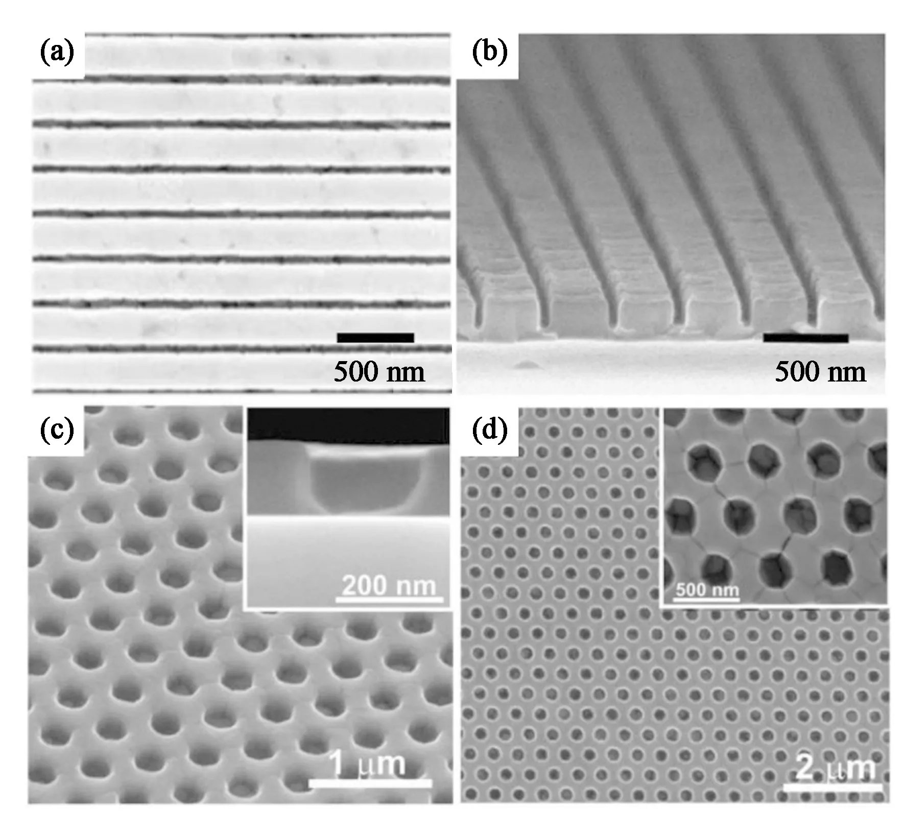
Fig.9 Nanoimprinted luminescent perovskite materials for OSL.(a,b) Top and cross section SEM images of the DFB grating imprinted into the MAPbI3 layer;(c) SEM image of the imprinted perovskite layer viewed under an angle of 45° (inset:cross-section);(d) Plan view SEM image of the imprinted perovskite layer (inset:magnified view).Reprinted with permission of Ref.[80],Copyright 2018 Optical Society of America and Ref.[82],Copyright 2017 WILEY-VCH Verlag GmbH &Co.KGaA,Weinheim,respectively.
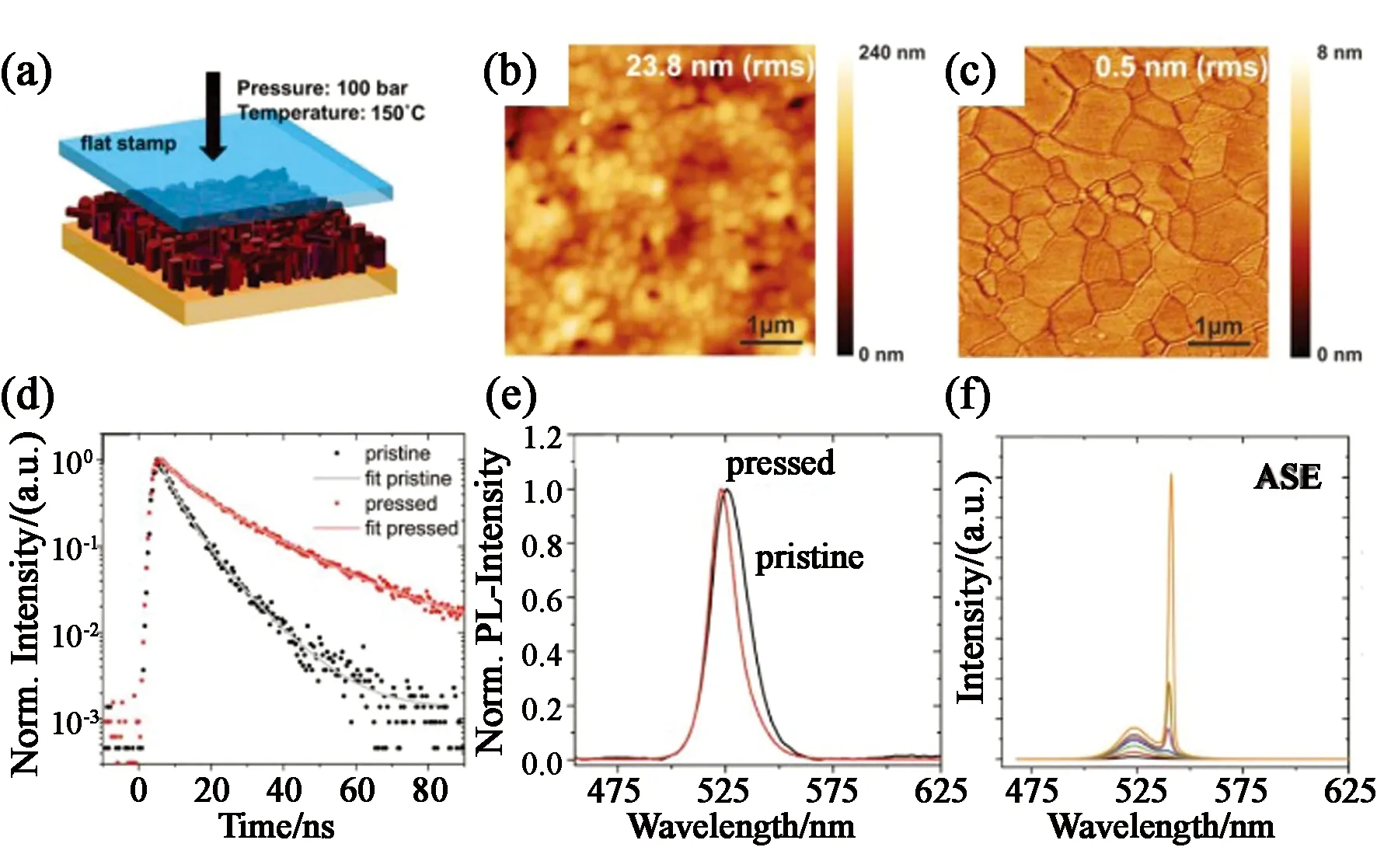
Fig.10 Effect of NIL on perovskite properties.(a) Schematic of the thermal imprint process using a flat silicon stamp.AFM images of layers before (b) and after (c) thermal imprint.The layer thickness is 120 nm.(d,e) Time-resolved photoluminescence (PL) decay and PL spectra for pristine (black) and pressed (red) layers at room temperature.Amplified spontaneous emission measurement on a flattened film:(f) emission spectra.Reprinted with permission of Ref.[84],Copyright 2019 WILEY-VCH Verlag GmbH &Co.KGaA,Weinheim.
4 Conclusions and Outlook
In this review,we have discussed the developments of NIL especially in the fields of OLEDs and OSLs.Different situations of imprinting and the role of nanoimprinted structures including nanostructured electrode,functional layers and encapsulation films in OLEDs have been analyzed.NIL introduces nanostructures into OLEDs with a simple,low-cost and high-precision process,which can improve the performance of light coupling and output of the device through the manipulation of light by the imprinted structures.Compared with the other review of nanostructured OLEDs,we have emphasized the NIL process for integrating the nanostructures.In terms of the OSLs,luminescent dye-doped polymers and self-luminescent materials have been introduced respectively.Moreover,a perovskite laser with excellent optoelectronic properties fabricated by NIL has been also concerned in this review.By combining low-threshold laser-active materials,such as perovskite,with the optimized optical gain cavity obtained by nanoimprint process,the output laser threshold can be significantly reduced.This exploration represents a major step toward the realization of electrically pumped lasing.As abovementioned developments of NIL on the OLEDs and OSLs,NIL will surely provide a strategy to fabricate the nanostructures on the organic optoelectronic devices not limited to OLEDs and OSLs.However,the lift-out of rigid mold and the suppression of deformation of soft mold need further study.
