Metallic Graphene Nanoribbons
2021-03-08ShengYiXieXianBinLi
Sheng‑Yi Xie, Xian‑Bin Li
ABSTRACT Isolated graphene nanoribbons (GNRs) usually have energy gaps, which scale with their widths, owing to the lateral quantum confinement effect of GNRs. The absence of metallic GNRs limits their applications in device interconnects or being one‑dimensional physics platform to research amazing properties based on metallicity. A recent study published in Science provided a novel method to produce metallic GNRs by inserting a symmetric superlattice into other semiconductive GNRs. This finding will broader the applications of GNRs both in nanoelectronics and fundamental science.
KEYWORDS Graphene; Nanoribbons; Quantum confinement effect; Supperlattice
Unlike the gapless semimetal of graphene [1], the graphene nanoribbons (GNRs) [2], whether armchair or zigzag type, usually own an energy gap scaling inversely with their widths due to the lateral quantum confinement effect of GNRs [3]. The raised energy gap, which is absent in gra‑phene, enables the production of transistor [4], yet the robust semicondutivity of GNRs limits the applications in such as device interconnects or being one‑dimensional physics plat‑form to explore superconductivity [5], Luttinger liquid [6], charge density waves [7] or spintronics [8]. Recently, one paper published inSciencereported an ingenious method to produce metallic GNRs [9] based on the atomically precise bottom‑up synthesis.
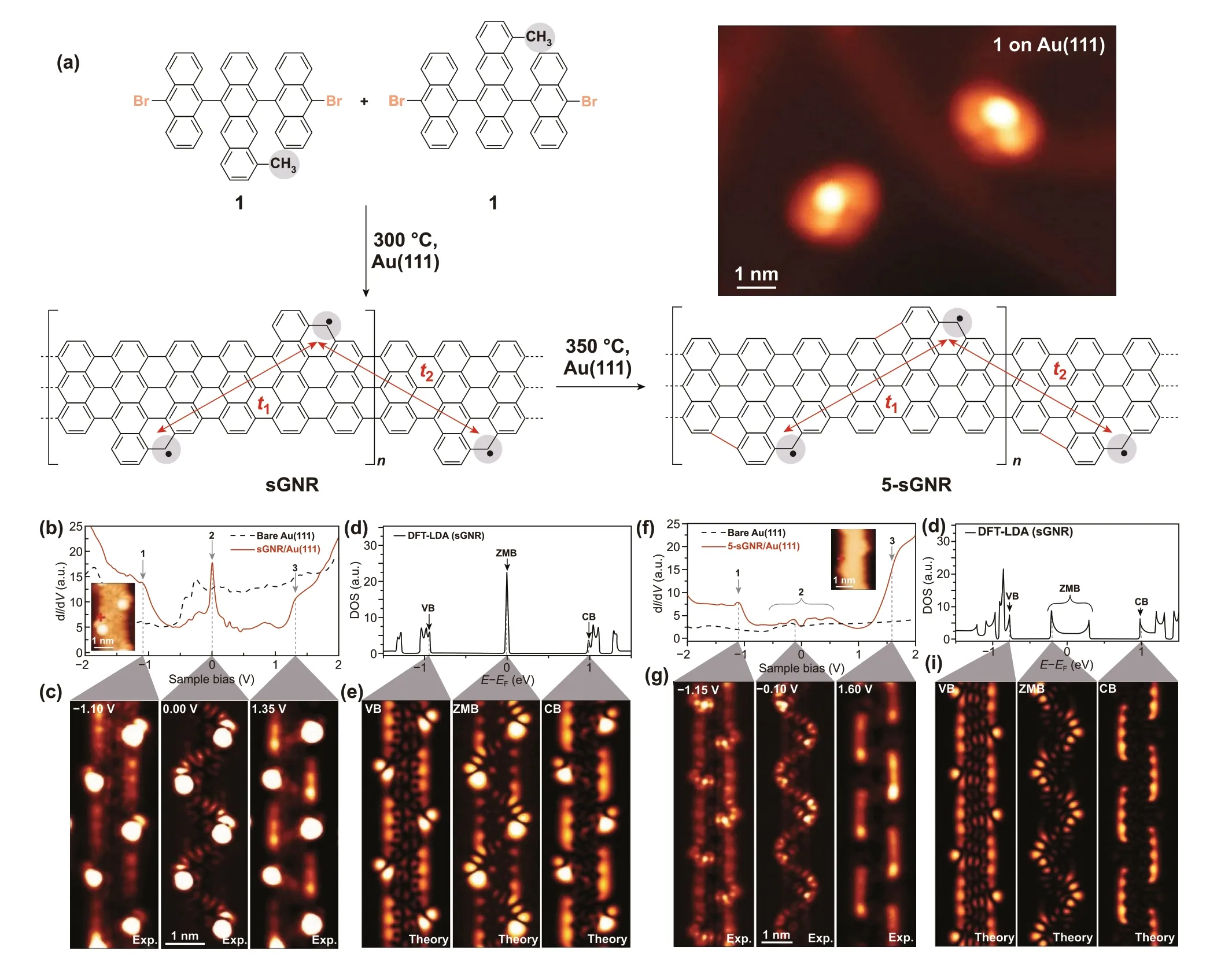
In this work, Rizzo et al. in University of California at Berkeley used the precursor molecule 1 (Fig. 1a) to construct the GNRs with the symmetrical insertion of methyl groups to form the superlattice, which are named as the sawtooth GNR (sGNR). Upon annealing over 350 ℃, the sGNRs transformed to the called five sawtooth sGNRs (5‑sGNRs) with minor chemical bond rearrangements to form a five‑membered ring along their edges, as also shown in Fig. 1a. Electronic structures of sGNRs and 5‑sGNRs were further determined both by scanning tunneling microscope (STM) spectroscopy and density functional theory (DFT) calcula‑tions. The experimental dI/dVpoint spectrum of a sGNR is shown in Fig. 1b, and the sharp peak states as well as their projection in real space (Fig. 1c) at the zero bias clearly show the metallic density of states (DOS), which agrees well with the DFT results (Fig. 1d, e). In their further experiment, the DOS of 5‑sGNRs spans a broader energy range around the Fermi level, inducing the robust metallicity with a 20‑fold increase of the metallic bandwidth, as shown in Fig. 1.
This work provides a smart strategy for realizing the metallicity in GNRs to act as a candidate used in logic devices. In future, as a direct measurement of metallicity, variable temperature conductivity experiments can be fur‑ther considered. Additionally, the performance comparison between these metallic GNRs and traditional metals like copper used in interconnect technology is also meaningful for the applications in nanoelectronics. Finally, considering the possible formation of junctions between these metal‑lic GNRs and ordinary semiconductive GNRs, whether Ohmic contact or Schottky contact can be formed should also deserve extra efforts.

Fig. 1 a Schematic bottom‑up growth of sGNRs and 5‑sCNRs from molecular precursor 1 on Au (111), and the inset at the top right corner shows STM topograph of two isolated monomers of precursor 1. b-e Electronic structure of sGNRs. b experimental dI/dV point spectroscopy, c related constant‑height dI/dV maps in real space, d DFT‑LDA calculated DOS, and e related local DOS maps of a sGNR. f-i Electronic structure of 5‑sCNRs. f experimental dI/dV point spectroscopy, g related constant‑height dI/dV maps, h DFT‑LDA calculated DOS, and i related local DOS maps of a 5‑sCNR. Reproduced from Ref. [9]. Copyright 2020 American Association for the Advancement of Science.
Open AccessThis article is licensed under a Creative Commons Attribution 4.0 International License, which permits use, sharing, adaptation, distribution and reproduction in any medium or format, as long as you give appropriate credit to the original author(s) and the source, provide a link to the Creative Commons licence, and indicate if changes were made. The images or other third party material in this article are included in the article’s Creative Com‑mons licence, unless indicated otherwise in a credit line to the material. If material is not included in the article’s Creative Com‑mons licence and your intended use is not permitted by statutory regulation or exceeds the permitted use, you will need to obtain permission directly from the copyright holder. To view a copy of this licence, visit http://creat iveco mmons.org/licen ses/by/4.0/.
杂志排行
Nano-Micro Letters的其它文章
- Laser Synthesis and Microfabrication of Micro/Nanostructured Materials Toward Energy Conversion and Storage
- Band Engineering and Morphology Control of Oxygen‑Incorporated Graphitic Carbon Nitride Porous Nanosheets for Highly Efficient Photocatalytic Hydrogen Evolution
- A Bulk‑Heterostructure Nanocomposite Electrolyte of Ce0.8Sm0.2O2‑δ–SrTiO3 for Low‑Temperature Solid Oxide Fuel Cells
- Present and Future of Phase‑Selectively Disordered Blue TiO2 for Energy and Society Sustainability
- Lotus Leaf‑Derived Gradient Hierarchical Porous C/MoS2 Morphology Genetic Composites with Wideband and Tunable Electromagnetic Absorption Performance
- Efficient Catalytic Conversion of Polysulfides by Biomimetic Design of “Branch‑Leaf” Electrode for High‑Energy Sodium–Sulfur Batteries
