Synthesis and photoelectric property of CdS nanocrystals decorated polyaniline nanowires
2021-01-11YOUZemengXIAOHaiqinZHOUWenhui
YOU Zemeng, XIAO Haiqin, ZHOU Wenhui*
(1.Institute of Oceanographic Instrumentation,Qilu University of Technology(Shandong Academy of Sciences), Qingdao 266000,Shandong,China;2.School of Materials,Henan University,Kaifeng 475004,Henan,China)
Abstract: By using thioglycolic acid(TGA)doped polyaniline(PANI)nanowires as sulfur source and matrix, CdS nanocrystals(NCs)decorated PANI nanowires were prepared via hydrothermal reaction.The morphology, crystal structure, valence state and photoelectric properties of the prepared CdS NCs decorated PANI nanowires were characterized by transmission electron microscopy(TEM), X-ray diffraction(XRD), X-ray photoelectron spectrum(XPS), UV-vis spectra and surface photovoltage spectroscopy(SPS).The CdS NCs with a size in the range of 5-10 nm were uniformly decorated on the surface of PANI nanowires.The photovoltage response measurement demonstrates the sprayed CdS NCs decorated PANI nanowires film can be used as p-n junction and photoelectric functional materials.
Keywords: CdS; nanocrystals; polyaniline; nanowires; hydrothermal reaction
Chalcogenides are of current interest in different areas due to their semiconducting properties and the ability to tailor their properties through careful control of synthesis conditions.Among these chalcogenides, CdS have received great attention because of its unique electrical and optic properties as well as extensive application in diverse areas.However, the main drawbacks of CdS lie in its low photogenerated electron-hole pair separation efficiency, which hinders its practical application.Therefore, some work had been devoted to resolving these drawbacks, such as combining CdS with graphene[1-3], carbon nanotubes[3-6], conductive polymers[7-8], TiO2nanotube[9]and graphtic carbon nitride[10].Polyaniline(PANI)is one kind of conducting polymers that has been extensively studied in the past few decades due to its applications in actuators, drug delivery systems, field emission displays, gas sensors and biosensors.PANI has been used as holes transport materials in light emitting diodes(LEDs)[11-12]and solar cells[13-14].
CdS is an n-type semiconductor, while PANI is a p-type semiconductor.So, it is expected that useful p-n junction or photoelectric functional nanocomposites can be created by combining PANI and CdS.In the past few years, several methods have been used to synthesis CdS-polyaniline nanocomposites[15-19].Herein, we report a facile, low-cost and available method for the preparation of CdS NCs decorated PANI nanowires(CdS/PANI).Transmission electron microscopy(TEM), X-ray diffraction(XRD), X-ray photoelectron spectrum(XPS), UV-Vis and surface photovoltage spectroscopy(SPS)characterizations confirm the morphology, crystal structure, valence state and photoelectric properties of the as-obtained CdS/PANI.The photocurrent response measurement indicates its potential application in photoelectric areas.
1 Experiments
1.1 Materials and chemicals
Aniline, Ammonium peroxydisulfate, Thioglycolic acid(TGA)and Cadmium chloride were all of analytical grade and used as received.All water used was obtained from a Millipore Milli-Q purification system.
1.2 Preparation of CdS/PANI
PANI nanowires which doped with HCl were prepared by in site oxidative polymerization of aniline in aqueous acid solution[20].The dedoped PANI nanowires were prepared by dispersed and stirred HCl doped PANI nanowires in 1.0 mol/L NH3·H2O for 2 h.Then, the dedoped PANI nanowires were dispersed and stirred in TGA solution contain 100 μL TGA overnight for TGA doping.CdS/PANI were prepared by reaction of TGA doped PANI nanowires with cadmium chloride under hydrothermal condition.In a typical procedure, 20 mg of TGA doped PANI nanowires and 73 mg cadmium chloride were added into 40 mL of water.After stirring for 10 min, the mixture was loaded into a Teflon-lined stainless steel autoclave of 50 mL capacity.The sealed autoclave was maintained at 120 ℃ for 10 h and then allowed to cool to room temperature.The precipitate was centrifuged and washed with deionized water.The final product was vacuum-dried at 60 ℃ before characterization.
1.3 Instruments and characterization
Transmission electron microscopy(TEM)observations were performed using a JEOL JEM-2010 microscope with an accelerating voltage of 200 kV.The phase and crystallographic structure of the product were identified by X-ray diffraction(XRD, Philips X’ Pert Pro, Cu-Kα).The UV-vis absorption spectra were obtained by using a UV-vis spectrometer(Perkin-Elmer, Lambda 35).X-ray photoelectron spectroscopy(XPS)measurements were carried out on an AXIS ULTRA spectrometer using Al KαX-ray as the excitation source.The photoelectrical property of the product was studied with the surface photovoltage spectroscopy(SPS, Stanford SR830).
2 Results and discussion
The color of reaction solution changed significantly at different steps, so the photograph(from left to right)of as-prepared HCl doped PANI nanowires, dedoped PANI nanowires, TGA doped PANI nanowires and CdS/PANI were collected and shown in Fig.1a.The freshly prepared PANI nanowires suspension is green(A).After dedoped by ammonia water, the color of the suspension changed to blue(DA).Then it became back to green after again after doped with TGA(TGA).This result indicated that TGA had been doped in the PANI matrix.The color or the final CdS/PANI is blue grey(10 h).The UV-vis absorption of as-prepared HCl doped PANI nanowires, dedoped PANI nanowires, TGA doped PANI nanowires and CdS/PANI were recorded and shown in Fig.1b.The UV-vis absorption spectrum of the freshly prepared PANI nanowires showed absorption bands at around 250, 430 and ≥ 800 nm.After dedoped by ammonia water, two obvious absorption bands centered at about 340 and 620 nm were observed.The TGA doped PANI nanowires shows absorption bands at 350 and 460 nm.The UV-vis absorption spectrum of CdS/PANI showed characteristic peaks at about 360 and 670 nm.The change of UV-vis absorption spectrum is consistent with that of color change of different samples.

Fig.1 Photograph(a)and UV-vis absorption(b)of asprepared HCl doped PANI nanowires, dedoped PANI nanowires, TGA doped PANI nanowires and CdS/PANI
In this work, CdS/PANI were prepared by reaction of TGA doped PANI nanowires and CdCl2under hydrothermal condition.The morphology of HCl doped PANI nanowires and final CdS/PANI were obtained by transmission electron microscopy.Fig.2a shows the TEM image of HCl doped PANI nanowires.The PANI nanowires show dendritic structure with relatively smooth surface, the diameter is in the range of 50-100 nm(red circles indicate CdS NCs).Because of the organic polymer nature of PANI, the contrast grade of HCl doped PANI nanowires is low.After hydrothermal reaction, some nanoparticles were uniformly decorated on the PANI nanowires matrix.These nanoparticles are CdS nanocrystals with size in the range of 5-10 nm(Fig.2b and Fig.2c).

Fig.2 TEM images of the PANI(a)and CdS/PANI(b and c)
Fig.3 shows the XRD patterns of CdS/PANI and CdS NCs prepared by chemical bath deposition method.The diffraction peaks at 2θ= 26.5°, 43.9° and 52.1° can be attributed to(111),(220)and(311)planes of CdS, respectively.The peak at about 28° is also characteristic peak of CdS-PANI nanocomposites[14].These results suggest that CdS NCs decorated on PANI nanowires are in cubic phase(JCPDS 10-454).Meanwhile, the broad diffraction peaks in the XRD patterns indicate the small particle size of CdS NCs.It can be noticed that the intensity of diffraction peaks from CdS/PANI are weak than that of CdS NCs prepared by chemical bath deposition.This result indicated that the decoration degree of CdS NCs was low in CdS/PANI.
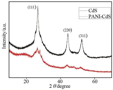
Fig.3 XRD patterns of the CdS NCs and CdS/PANI
XPS analysis was used to study the valence states of main elements(Cd/S/C)in CdS/PANI(Fig.4).The survey XPS spectrum of the CdS/PANI is shown in Fig.4a, which indicates the presence of Cd, S, C and O as well.Most of the peaks can be attributed to the elements from materials and reagents used in synthesis process.The C and O are likely due to TGA and/or the contamination as a result of the sample exposure to atmosphere.High-resolution XPS spectra of the three main elements(Cd 3d, S 2p and C 1s)are shown in Figs.4b-4d.The peak of Cd 3d(Fig.4b)is split into 403.8 eV(3d3/2)and 410.6 eV(3d1/2)with a split orbit of 6.8 eV, which is in good accordance with the value of Cd(Ⅱ).The S 2p(Fig.4c)core-level also shows the spin orbit components corresponding to 2p3/2(160.1 eV)and 2p1/2(161.6 eV).It should be noted that there is a shift in the S 2p core-level peaks to lower binding energy.This phenomenon could be attributed to the formation of Cd-S bond.When metal interacts with sulfur, redistribution of electronic density occurs as a result of valence electrons shifting from metal to sulfur, resulting in noticeable variations of electronic structure of inner shells of cation and anion[21].In the present case, the XPS binding energies of Cd 3d and S 2p are indicative of CdS.Another weak broad peak centered at about 166~167 eV may be ascribed to the oxidized sulfur species such as sulfonate[22].The detected peak of C 1s of CdS/PANI could be attributed to C-C bond and C-N bond(Fig.4d).
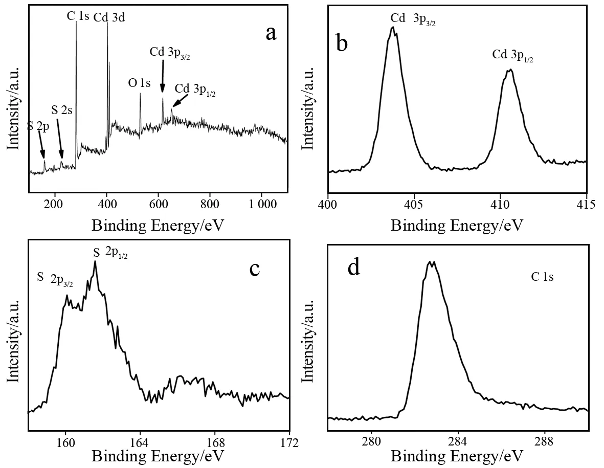
Fig.4 XPS analysis of survey spectra(a), Cd 3d(b), S 2p(c)and C 1s(d)for CdS/PANI
Surface photovoltage technique is an effectively way to study the process of photoinduced charge separation and transfer, and the intensity of the photovoltage is known to be primarily dependent on the degree of separation of the photogenerated charges[23].The CdS/PANI film was fabricated onto ITO glass by spray method.Photograph of HCl doped PANI nanowires film and CdS/PANI film obtained by spray method.SPS measurements were carried out with a solid-junction photovoltaic ITO/sample/ITO sandwich structure.As shown in Fig.5, the SPS signal of the CdS/PANI film was enhanced significantly compared to that of HCl doped PANI nanowires.Enhanced SPS signal of the CdS/PANI film indicates high chargeseparation efficiency in CdS/PANI.This result also indicates the formation of p-n junction between CdS NCs and PANI nanowires matrix.The highly enhanced SPS signal indicated high efficiency photogenerated carrier separation, thus great potential use of CdS/PANI in photoelectric area.

Fig.5 Surface photovoltage spectra of HCl doped PANI nanowires and CdS/PANI
3 Conclusions
In summary, we have successfully achieved synthesis of CdS/PANI by a simple hydrothermal method using doped TGA as sulfur source.This method affords an effective route to decorate chalcogenide nanocrystals on the surface of PANI nanowires.The facile preparation and low cost of the current method show it has bright application prospects in photoelectric areas in the future.