Optical and electrical properties of gallium-doped zinc magnesium oxide transparent conductive thin films
2020-12-22GUJinhuaZHUYaKANGHuaiLONGHao
GU Jinhua, ZHU Ya, KANG Huai, LONG Hao*
(1 Experimental Teaching and Laboratory Management Center, South-Central University for Nationalities, Wuhan 430074, China;2 College of Electronic Information Engineering, South-Central University for Nationalities, Wuhan 430074, China)
Abstract Transparent conducting thin films of gallium-doped zinc magnesium oxide were deposited by magnetron sputtering onto glass substrates. The effects of working pressure on the optical and electrical properties of the deposited films were investigated by ultraviolet-visible spectrophotometer and Hall effect measurement system. The results show that the working pressure significantly affects the electrical and optical characteristics of the deposited films. The sample fabricated at the working pressure of 3.6 Pa possesses the best optoelectrical performance, with the lowest resistivity of 1.54×10⁻³ Ω·cm, the maximum average visible transmittance of 87.72% and the highest figure of merit of 4.72×10³ Ω-1·cm-1. The direct energy gaps were determined by extrapolation method and the obtained values are larger than that of undoped zinc oxide.
Keywords doped zinc oxide; transparent conductive oxide;thin film;magnetron sputtering
The thin films of Sn-doped In2O3(ITO) are widely used as a transparent conductive oxide (TCO) electrodes in flat-panel displays (FPDs), photovoltaic solar cells (PSCs), thin film transistors (TFTs) and light-emitting diodes (LEDs)[1-5]due to their characteristics of high visible transmittance, low electrical resistivity and superior substrate adhesion[6-9]. Presently, zinc oxide (ZnO) has been actively investigated as an alternate material to replace ITO due to its inherent characteristics such as abundant raw materials, large excitation binding energy, wide band gap and high radiation resistance[10-13]. It is used in various technological domains such as FPDs, PSCs, LEDs, TFTs, photodetectors and laser diodes[14-20]. B, Al, Ga, Zr, Mg, Ti, Mn and rare earth-doped ZnO-based TCO thin films have been investigated[21-30]. In singly-doped ZnO thin films, Ga doping has several advantages in terms of conductivity and humidity durability, while Mg-doped ZnO hin films have superb properties for the transmission and optical band gap[31-34]. In this paper, the Ga-doped zinc magnesium oxide TCO thin films were deposited by magnetron sputtering technique at different working pressures, and the optical and electrical properties of the deposited thin films were investigated.
1 Experimental
The thin film samples were grown onto glass substrates by magnetron sputtering system (MS-560C) from a Ga2O3∶MgO∶ZnO (2 wt.%∶2 wt.%∶96 wt.%) ceramic target with a base pressure of 3.0×10⁻⁴Pa. High-purity argon gas (purity of 99.999 %) was used as the working gas. The glass substrates were carefully cleaned in acetone and alcohol each for about 15 min using an ultrasonic cleaning process, and finally washed by de-ionized water. In order to study the influence of working pressure on the characteristics of the deposited samples, the argon pressure was adjusted to be in the range of 3.2 Pa to 4.0 Pa in the experiment. The deposition parameters for preparing the thin film samples are listed in Table 1.
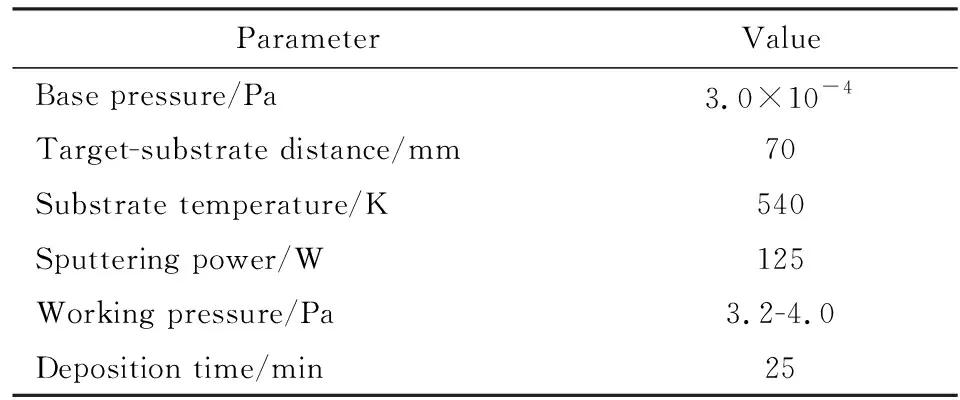
Tab.1 The deposition parameters of thin film samples表1 薄膜样品的制备工艺参数
The transmittance(T) and absorbance (A) spectra of the deposited samples were measured at room temperature with a double-beam ultraviolet-visible spectrophotometer (TU-1901) in the wavelength (λ) region of 300-800 nm, with a step size of 1 nm. The Hall mobility (μ), carrier concentration (ne) and resistivity (ρ) of the samples were measured using a Hall effect measurement system (RH-2035) by the Van der Pauw method at room temperature.
2 Results and discussion
Fig.1 presents the variation ofTas a function ofλfor all the thin films. As can be seen, all theT-λcurves exhibit the interference pattern with sharp fall of transmittance at the band-edge region. The result implies that the deposited samples have low surface roughness and good crystal quality[6,8,21].
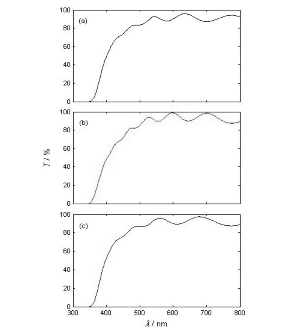
Fig.1 The T-λ curves of samples prepared at working pressure of (a) 3.2 Pa, (b) 3.6 Pa and (c) 4.0 Pa, respectively图1 工作压强为(a) 3.2 Pa, (b) 3.6 Pa和(c) 4.0 Pa时薄膜样品的T-λ曲线
As shown in Fig.2, the average transmittance in the visible range (Tav) increases with the working pressure up to 3.6 Pa, and then decreases when the working pressure is over 3.6 Pa. When the working pressure is 3.6 Pa, the highestTavvalue of 87.72% can be obtained. The enhancement of optical transmission is closely related to the improvement of crystalline quality of the deposited films.

Fig.2 Effect of working pressure on Tav of the samples图2 工作压强对薄膜样品Tav的影响
Fig.3 displays the variation of absorbance (A) as a function ofλfor all the thin film samples. As can be seen, theAvalues of the samples are very small at long wavelengths, indicating that the prepared samples are highly transparent. Note also that the curves of theAare fairly flat above 430 nm and increase rapidly at shorter wavelength. TheAvalues are observed to be in the range of 0.0399~0.0725 for the deposited samples when the wavelengthλ=500 nm.

Fig.3 The A-λ curves of samples prepared at working pressure of (a) 3.2 Pa, (b) 3.6 Pa and (c) 4.0 Pa, respectively图3 工作压强为(a) 3.2 Pa, (b) 3.6 Pa和(c) 4.0 Pa时薄膜样品的A-λ曲线
The absorption coefficients (α) are calculated from the measuredAvalues by the following equation[35]:
(1)
wheredis the film thickness of the deposited samples. In order to determine the optical band gap (Eg) of the direct transitions, the Tauc method was used[21,36]. In this method, the following formulae were used to calculate the band gapEgof the prepared samples.
(α·hν)2=B(hν-Eg),
(2)
(3)
whereBis an energy-independent constant,λis the wavelength of incident light,his the Planck constant (h=6.63×10⁻³⁴J·s),νis the frequency of incident photon,cis the velocity of light (c=3.0×10⁸m/s),hνis the photon energy. In Fig.4, (αhν)2versushνplots of the prepared samples are presented with the linear section of the plot extrapolated to (αhν)2=0, to intersect the photon energy (hν) axis. The value of energyhνat this point defines the optical band gap energy,Eg. The direct band gaps of all the samples were estimated by extrapolation method. The obtainedEgvalues of all the samples are shown in Fig.5. Note that theEgincreases with working pressure up to 3.6 Pa from 3.41 eV to 3.44 eV. Then it decreases to 3.42 eV at working pressure of 4.4 Pa. Obviously, the obtainedEgvalues of the deposited samples are larger than that of pure ZnO (3.27 eV).
The refractive index (n) of the prepared thin films can be calculated by the following equation[37,38]:
(4)
For the samples fabricated at the working pressure of 3.2 Pa, 3.6 Pa and 4.0 Pa, thenvalues are obtained to be about 2.58, 2.56 and 2.57, respectively. Clearly, the refractive indexnof the samples is hardly affected by the working pressure.
Fig.6-Fig.8 show the values ofne,μandρfor all the deposited samples. As the working pressure increases from 3.2 Pa to 3.6 Pa, bothneandμincrease, which leads to the decrease ofρof the deposited samples. When the working pressure is 3.6 Pa, the deposited film exhibits the lowestρof 1.54×10⁻³Ω·cm. The lowestρvalue at 3.6 Pa can be attributed to the improvement of crystal quality. In addition, the highestμof 7.46 cm2V-1s-1and the maximumneof 5.23×1020cm-3are also observed when the working pressure is 3.6 Pa.

Fig.4 The (αhν)2-hν curves of samples prepared at working pressure of (a) 3.2 Pa, (b) 3.6 Pa and (c) 4.0 Pa, respectively图4 工作压强为(a) 3.2 Pa, (b) 3.6 Pa和(c) 4.0 Pa时薄膜样品的(αhν)2-hν曲线

Fig.5 Effect of working pressure on Eg of the samples图5 工作压强对薄膜样品Eg的影响
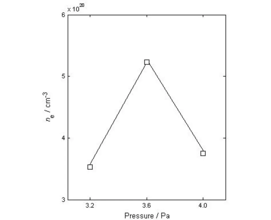
Fig.6 Effect of working pressure on ne of the samples图6 工作压强对薄膜样品ne的影响

Fig.7 Effect of working pressure on μ of the samples图7 工作压强对薄膜样品μ的影响
In order to quantify the optoelectrical properties of the deposited samples, the figure of merit (FH) was calculated by the following formula[39]:
(5)
whereρis the resistivity, andTavis the average visible transmittance. TheFHvalues of all the deposited samples are shown in Fig.9. TheFHrises first and subsequently falls with the increment of working pressure, the sample deposited at 3.6 Pa possesses the highestFHvalue of 4.72×10³Ω-1·cm-1. Thus, it can be concluded that the optimal working pressure is 3.6 Pa in the present study.
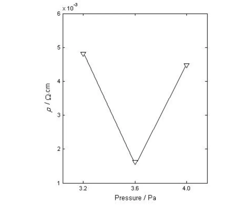
Fig.8 Effect of working pressure on ρ of the samples图8 工作压强对薄膜样品ρ的影响
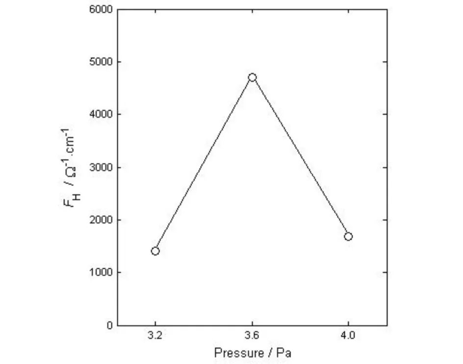
Fig.9 Effect of working pressure on FH of the samples图9 工作压强对薄膜样品FH的影响
3 Conclusions
In summary, the Ga-doped zinc magnesium oxide TCO thin films were deposited onto the glass substrates using the magnetron sputtering technique. The influences of working pressure on the optical and electrical properties of the deposited films were investigated. The optical and electrical properties of the samples are observed to be subjected to the working pressure. The lowest resistivity (1.54×10⁻³Ω·cm), the maximum average visible transmittance (87.72%) and the highest figure of merit (4.72×10³Ω-1·cm-1) are obtained when the working pressure is 3.6 Pa. In addition, the optical band gaps were calculated by extrapolation method and observed to be in the range of 3.41-3.44 eV. The results indicate that the working pressure is one of the most important deposition parameters to affect the optoelectrical properties of doped ZnO thin films.